Table of Contents
Advertisement
Quick Links
Advertisement
Table of Contents

Related Manuals for Advantech PCI-1751


Summary of Contents for Advantech PCI-1751
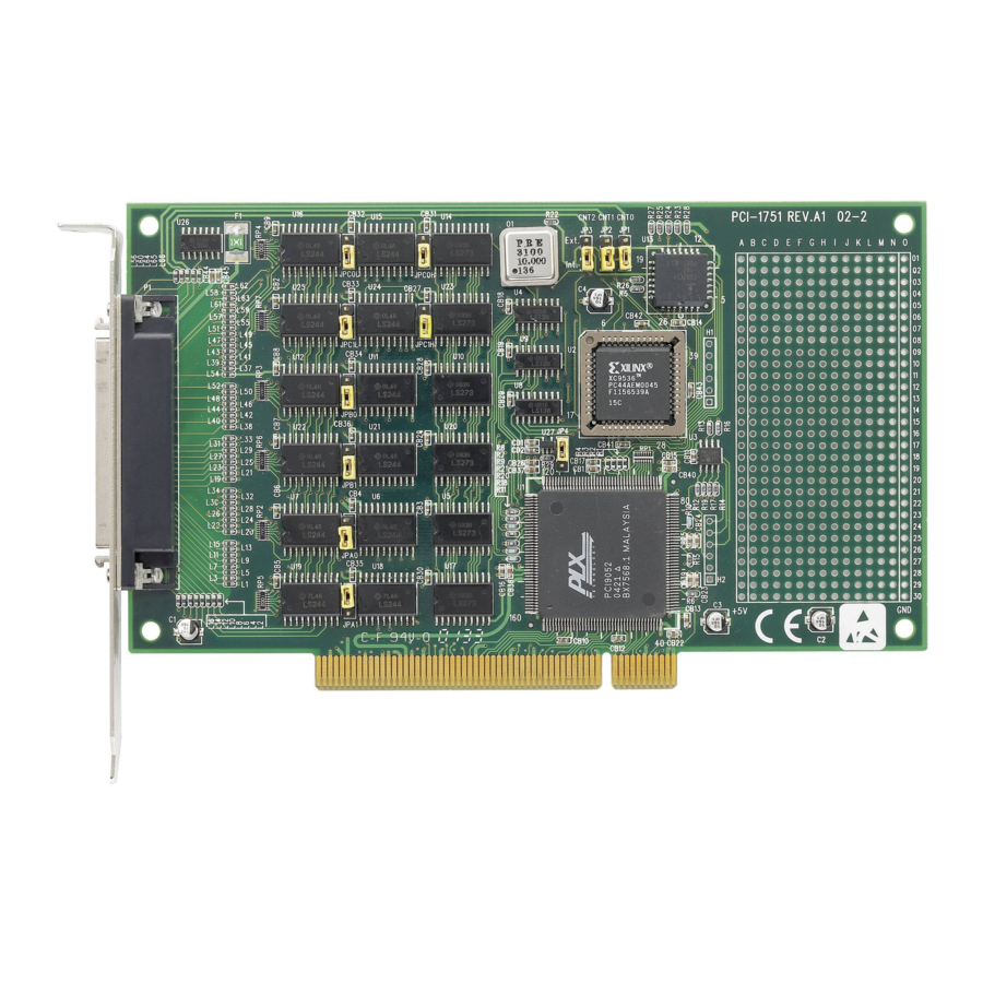
- Page 1 User Manual PCI-1751 48-bit Digital Input/ Output Card for PCI Bus...
- Page 2 No part of this manual may be reproduced, copied, translated or transmitted in any form or by any means without the prior written permission of Advantech Co., Ltd. Information provided in this manual is intended to be accurate and reliable. How- ever, Advantech Co., Ltd.
- Page 3 This product has passed the CE test for environmental specifications when shielded cables are used for external wiring. We recommend the use of shielded cables. This kind of cable is available from Advantech. Please contact your local supplier for ordering information.
- Page 4 Technical Support and Assistance Visit the Advantech web site at http://support.advantech.com where you can find the latest information about the product. Contact your distributor, sales representative, or Advantech's customer service center for technical support if you need additional assistance. Please have the following information ready before you call: –...
- Page 5 The sound pressure level at the operator's position according to IEC 704-1:1982 is no more than 70 dB (A). DISCLAIMER: This set of instructions is given according to IEC 704-1. Advantech disclaims all responsibility for the accuracy of any statements contained herein.
- Page 6 Don't touch any components on the CPU card or other cards while the PC is on. Disconnect power before making any configuration changes. The sudden rush of power as you connect a jumper or install a card may damage sensitive elec- tronic components. PCI-1751 User Manual...
-
Page 7: Table Of Contents
Table A.2: Digital Output............20 Table A.3: Counter / Timer............20 Table A.4: General Specifications..........20 Appendix B Block Diagram ........21 PCI-1751 Block Diagram................. 22 Appendix C Function of 8254 Counter Chip ..23 The Intel 8254 ..................24 Counter Read/Write and Control Registers..........24 Counter Operating Modes............... - Page 8 Counter Operations................. 27 C.4.1 Read/Write Operation ..............27 C.4.2 Counter Read-back Command ........... 27 C.4.3 Counter Latch Operation ............28 Counter Applications................28 Appendix D Register of PCI-1751 ......29 Register Format of PCI-1751 ..............30 PCI-1751 User Manual viii...
-
Page 9: Chapter 1 General Information
Chapter General Information... -
Page 10: Introduction
Two other features give the PCI-1751 practical advantages in an industrial setting. When the system is hot reset (the power is not turned off) the PCI-1751 retains the last I/O port settings and output values if the user has set jumper JP4 to enable this feature. -
Page 11: Installation Guide
Installation Guide Before you install your PCI-1751 card, please make sure you have the following nec- essary components: PCI-1751 card PCI-1751 User's Manual Advantech driver DAQNavi (included in the CD-ROM) Wiring cable PCL-10168 (optional) Wiring board ADAM-3968 (optional) ... - Page 12 PCI-1751 User Manual...
-
Page 13: Chapter 2 Installation
Chapter Installation... -
Page 14: Unpacking
Unpacking After receiving your PCI-1751 package, please inspect its contents first. The package should contain the following items: PCI-1751 card Companion CD-ROM (Device Drivers included) Startup Manual The PCI-1751 card harbors certain electronic components vulnerable to electrostatic discharge (ESD). -
Page 15: Hardware Installation
Touch the metal part on the surface of your computer to neutralize the static electricity that might be on your body. Insert the PCI-1751 card into a PCI slot. Hold the card only by its edges and carefully align it with the slot. Insert the card firmly into place. Use of excessive force must be avoided, otherwise the card might be damaged. - Page 16 PCI-1751 User Manual...
-
Page 17: Chapter 3 Signal Connections
Chapter Signal Connections... -
Page 18: Overview
PCI-1751 via the I/O connector. Switch and Jumper Settings We designed the PCI-1751 with ease-of-use in mind. It is a "plug and play" card, i.e. the system BIOS assigns the system resources such as base address and interrupt automatically. - Page 19 Jumper JP4 gives the PCI-1751 a new and valuable capability. With JP4 enabled, the PCI-1751 "memorizes" all port I/O settings and output values, and, in the event of a "hot" reset, the settings and output values present at the port just prior to reset are restored to each port following reset.
-
Page 20: Pin Assignments
CNT0_G, CNT1_G and CNT2_G: Gate control pins of Counter / Timer 0, 1 and 2 INT_OUT: Interrupt output. This pin changes to logic 1 whenever the PCI-1751 generates an interrupt, and returns to logic 0 when the interrupt is cleared. GND: Ground... -
Page 21: Digital I/O Ports
Digital I/O Ports Introduction The PCI-1751 emulates two 8255 programmable peripheral interface (PPI) chips in mode 0, but with higher driving capability than a standard 8255 chip. Each of the 8255 chips has 24 programmable I/O pins that are divided into three 8-bit ports. The total 48 DI/O pins from both chips are divided into 6 ports, designated PA0, PB0, PC0, PA1, PB1 and PC1. - Page 22 (> 1.5 k Ω). It is advisable to connect a 1.5 k Ω resistor in parallel with such a voltage source to avoid a voltage rise inside the voltage source. PCI-1751 User Manual...
-
Page 23: Timer/Counter Operation
Timer/Counter Operation Introduction The PCI-1751 includes one 8254 compatible programmable timer/counter chip which provides three 16-bit counters, designated as Timer 0, Timer1 and Counter 2. Each has 6 operation modes. Timer 0 and Timer 1 can be used separately or can be cas- caded to create one 32-bit timer. -
Page 24: Interrupt Function
Counter 2) are connected to the interrupt circuitry. The "Interrupt Control Regis- ter" of the PCI-1751 controls how the combination of the 6 signals generates an inter- rupt. Two interrupt request signals can be generated at the same time, and then the software can service these two request signals by ISR. - Page 25 This bit must be cleared in the ISR to service the next incoming interrupt. Table 3.7: Interrupt Flag Bit Values F0 & F1 Interrupt status Read Interrupt exists No interrupt Write Clear interrupt Don’t care PCI-1751 User Manual...
- Page 26 PCI-1751 User Manual...
-
Page 27: Appendix A Specifications
Appendix Specifications... -
Page 28: Pci-1751 Specifications
A (max.) Operating: 0 ~ +70 (32 ~ 158 Temperature Storage: -20 ~ +80 (-4 ~ 176 Relative Humidity 5 – 95 % RH non-condensing (refer to IEC 60068-2-3) Certifications CE / FCC PCI-1751 User Manual... -
Page 29: Appendix B Block Diagram
Appendix Block Diagram... -
Page 30: Pci-1751 Block Diagram
PCI-1751 Block Diagram PCI-1751 User Manual... -
Page 31: Appendix C Function Of 8254 Counter Chip
Appendix Function of 8254 Counter Chip... -
Page 32: The Intel 8254
10 MHz input frequencies to the counter chip from an on-board crystal oscillator. On the PCI-1751, the 8254 chip's Timer 0 and Timer 1 can be used separately or can be cascaded to create a 32-bit programmable timer by setting JP2. When the clock source of Timer 1 is from an external source, you can user Timer 0 and Timer 1 as two independent 16-bit timers. - Page 33 If you set both SC1 and SC0 to 1 and STA to 0, the register selected by C2 to C0 contains a byte which shows the status of the counter. The data format of the counter read/write register then becomes: PCI-1751 User Manual...
-
Page 34: Counter Operating Modes
This is accomplished by decreasing the counter by two on the falling edge of each clock pulse. When the counter reaches the terminal count, the state of the output is changed, the counter is reloaded with the full count and the whole pro- cess is repeated. PCI-1751 User Manual... -
Page 35: Mode 4 - Software Triggered Strobe
STA bit = 0. The status must be latched to be read; the status of a counter is accessed by a read from that counter. The counter status format appears at the beginning of the chapter. PCI-1751 User Manual... -
Page 36: Counter Latch Operation
Counter Applications The 8254 compatible programmable interval timer/counter on your PCI-1751 inter- face card is a a very useful device. You can program timers 1 and 2 to serve as tim- ers, event counters, square wave genera- tors, or as a watchdog to generate regular interrupts at a fixed interval. -
Page 37: Register Of Pci-1751
Appendix Register of PCI-1751... -
Page 38: Register Format Of Pci-1751
Register Format of PCI-1751 Function Base Address + (Decimal) Read Write Port A0 Port A0 Port B0 Port B0 Port C0 Port C0 Reserved Port 0 Configuration Port A1 Port A1 Port B1 Port B1 Port C1 Port C1 Reserved... - Page 39 PCI-1751 User Manual...
- Page 40 No part of this publication may be reproduced in any form or by any means, electronic, photocopying, recording or otherwise, without prior written permis- sion of the publisher. All brand and product names are trademarks or registered trademarks of their respective companies. © Advantech Co., Ltd. 2015...
Need help?
Do you have a question about the PCI-1751 and is the answer not in the manual?
Questions and answers