Table of Contents
Advertisement
Quick Links
Download this manual
See also:
User Manual
Copyright
This documentation and the software included with this product are
copyrighted 2002 by Advantech Co., Ltd. All rights are reserved.
Advantech Co., Ltd. reserves the right to make improvements in the
products described in this manual at any time without notice. No part of this
manual may be reproduced, copied, translated or transmitted in any form or
by any means without the prior written permission of Advantech Co., Ltd.
Information provided in this manual is intended to be accurate and reliable.
However, Advantech Co., Ltd. assumes no responsibility for its use, nor for
any infringements of the rights of third parties which may result from its
use.
Acknowledgments
PC-LabCard is a trademark of Advantech Co., Ltd. IBM and PC are
trademarks of International Business Machines Corporation. MS-DOS,
Windows, Microsoft Visual C++ and Visual BASIC are trademarks of
Microsoft Corporation. Intel and Pentium are trademarks of Intel
Corporation. Delphi and C++ Builder are trademarks of Inprise
Corporation.
CE notification
The PCI-1730/1733/1734, developed by ADVANTECH CO., LTD., has
passed the CE test for environmental specifications when shielded cables
are used for external wiring. We recommend the use of shielded cables. This
kind of cable is available from Advantech. Please contact your local
supplier for ordering information.
On-line Technical Support
For technical support and service, please visit our support web site
Note:
Concerning the environment protection, we'd like to reduce the paper
using for the user's manual. Starting the page of Appendix C, please find
the PDF file of the CD-ROM.
Part No. 2003173000
Printed in Taiwan
1
1st Edition
April 2002
Advertisement
Table of Contents

Related Manuals for Advantech PCI-1730


Summary of Contents for Advantech PCI-1730
- Page 1 No part of this manual may be reproduced, copied, translated or transmitted in any form or by any means without the prior written permission of Advantech Co., Ltd. Information provided in this manual is intended to be accurate and reliable.
-
Page 3: Table Of Contents
Contents 1. INTRODUCTION........................1 1.1 F ........................1 EATURES 1.2 A ......................... 5 PPLICATIONS 1.3 I ...................... 5 NSTALLATION UIDE 1.4 S ..................... 7 OFTWARE VERVIEW 1.5 D ..............8 EVICE RIVERS ROGRAMMING OADMAP 1.6 A ........................ 10 CCESSORIES 2. INSTALLATION........................11 2.1 U ........................ -
Page 5: Introduction
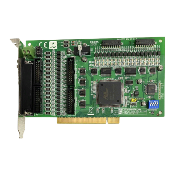
For easy monitoring, each isolated digital input channel is equipped with one red LED, and each isolated digital output channel is equipped with one green LED to show its ON/OFF status. The PCI-1730 and PCI- 1733’s isolated digital input channels are ideal for digital input in noisy environments or with floating potentials. - Page 6 Keep digital output values when hot system reset High ESD protection (2,000 V High over-voltage protection (70 V Wide input range (5 ~ 30 V Board ID PCI-1733 Compatible as PCL-733 32 isolated Digital Input channels High output driving capacity High-voltage isolation on isolated Input channels (2,500 V Interrupt handling capability D-type connector for isolated input channels...
- Page 7 Wide Input Range The PCI-1730/1733 has a wide range of input voltage from 5 to 30 V and it is suitable for most industrial applications with 12 V , 24 V...
- Page 8 Reset Protection Fulfills Requirement for Industrial Applications When the system has undergone a hot reset (i.e. without turning off the system power), the PCI-1730/1734 can either retain outputs values of each channel, or return to its default configuration as open status, depending on its on-board jumper setting.
-
Page 9: Applications
BCD interfacing Digital I/O control Industrial and lab automation Laboratory & Education 1.3 Installation Guide Before you install your PCI-1730/1733/1734 card, please make sure you have the following necessary components: PCI-1730/1733/1734 card PCI-1730/1733/1734 User’s Manual Driver software Advantech DLL drivers... - Page 10 Install Driver from CD-ROM, then power-off PC Install Hardware and power-on PC Use driver utility to configure hardware Use test utility to test hardware Read examples & driver manual Start to write your own application Fig. 1-1 Installation Flow Chart...
-
Page 11: Software Overview
Device Drivers The Advantech Device Drivers software is included on the companion CD-ROM at no extra charge. It also comes with all the Advantech DA&C cards. Advantech’s DLL driver features a complete I/O function library to help boost your application performance. The... -
Page 12: Device Drivers Programming Roadmap
1.5 Device Drivers Programming Roadmap This section will provide you a roadmap to demonstrate how to build an application from scratch using Advantech Device Drivers with your favorite development tools such as Visual C++, Visual Basic, Delphi and C++ Builder. The step-by-step instructions on how to build your own applications using each development tool will be given in the Device Drivers Manual. - Page 13 Device Drivers Manual. Programming with Device Drivers Function Library Advantech Device Drivers offers a rich function library to be utilized in various application programs. This function library consists of numerous APIs that support many development tools, such as Visual C++, Visual Basic, Delphi and C++ Builder.
-
Page 14: Accessories
1.6 Accessories Advantech offers a complete set of accessory products to support the PCI-1730/1733/1734 card. These accessories include: Wiring Cable PCL-10137 The PCL-10137 shielded cable is specially designed for PCI-1730/1733/1734 cards to provide high resistance to noise. To achieve a better signal quality, the signal wires are twisted in such a way as to form a “twisted-pair cable”, reducing cross-talk and noise... -
Page 15: Installation
This chapter gives users a package item checklist, proper instructions about unpacking and step-by-step procedures for both driver and card installation. 2.1 Unpacking After receiving your PCI-1730/1733/1734 package, please inspect its contents first. The package should contain the following items: ! PCI-1730/1733/1734 card ! Companion CD-ROM (Device Drivers included) ! User’s Manual... - Page 16 Also pay extra caution to the following aspects to ensure proper installation: ! Avoid physical contact with materials that could hold static electricity such as plastic, vinyl and Styrofoam. ! Whenever you handle the card, grasp it only by its edges. DO NOT TOUCH the exposed metal pins of the connector or the electronic components.
-
Page 17: Driver Installation
1730/1733/1734 card into your system, since this will guarantee a smooth installation process. The Advantech Device Driver Setup program for the PCI- 1730/1733/1734 card is included on the companion CD-ROM that is shipped with your DA&C card package. Please follow the steps below to install the driver software: Step 1: Insert the companion CD-ROM into your CD-ROM drive. -
Page 18: Hardware Installation
(please refer to 2.2 Driver Installation) After the device driver installation is completed, you can now go on to install the PCI-1730/1733/1734 card in any PCI slot on your computer. But it is suggested that you should refer to the computer user manual or related documentation if you have any doubt. - Page 19 Step 4: Touch the metal part on the surface of your computer to neutralize the static electricity that might be on your body. Step 5: Insert the PCI-1730/1733/1734 card into a PCI slot. Hold the card only by its edges and carefully align it with the slot. Insert the card firmly into place.
- Page 20 Fig. 2-3 The device name listed on the Device Manager Note: If your card is properly installed, you should see the device name of your card listed on the Device Manager tab. If you do see your device name listed on it but marked with an exclamation sign “!”, it means your card has not been correctly installed.
-
Page 21: Device Setup & Configuration
2.4 Device Setup & Configuration The Advantech Device Manager program is a utility that allows you to set up, configure and test your device, and later stores your settings on the system registry. These settings will be used when you call the APIs of Advantech Device Drivers. - Page 22 Fig. 2-5 The “Device(s) Found” dialog box Configuring the Device Step 4: On the PCI-1730 Device Setting dialog box (Fig. 2-6), you can configure the IDI00, IDI01 and DI00, DI01 Interrupt trigger mode either as Rising Edge or Falling Edge, and Enable or Disable the IDI00, IDI01 and DI00, DI01.
- Page 23 Fig. 2-7 The Device Name appearing on the list of devices box Note: As we have noted, the device name “000:<PCI-1730 BoardID=0 I/O=1000H>” begins with a device number “000”, which is specifically assigned to each card. The device number is passed to the driver to specify which device you wish to control.
-
Page 25: Signal Connections
PC and other hardware devices. This chapter provides useful information about how to connect input and output signals to the PCI-1730/1733/1734 via the I/O connector. 3.2 Switch and Jumper Settings PCI-1730 The PCI-1730 card has two function jumper settings. - Page 26 Complete loss of power to the chip clears the chip memory. Thus, no matter how JP2 is set, if the power to the PCI-1730 is disconnected, the digital output channel’s initial power-on state will be "OFF".
- Page 27 PCI-1733 Fig. 3-2 Card connector, jumper and switch locations Board ID setting BD3 BD2 BD1 BD0 Board ID Note: On: 1, Off: 0...
- Page 28 PCI-1734 The PCI-1734 card has one function jumper setting. Fig. 3-3 Card connector, jumper and switch locations Table 3-3: Summary of jumper settings Names of Jumpers Function description Keep last status after hot reset Default configuration Setting the time to reset the digital outputs Some users will want the capability of clearing each digital output when the system (or PC) issues a reset signal on the PCI bus.
- Page 29 Complete loss of power to the chip clears the chip memory. Thus, no matter how JP2 is set, if the power to the PCI-1734 is disconnected, the digital output channel’s initial power-on state will be "OFF". Board ID setting BD3 BD2 BD1 BD0 Board ID Note: On: 1, Off: 0...
-
Page 30: Signal Connections
3.3 Signal Connections PCI-1730 (JP4, JP5: REV.A1) Pin Assignments IDO 0 IDO 1 IDI 0 IDI 1 IDO 2 IDO 3 IDI 2 IDI 3 IDO 4 IDO 5 IDI 4 IDI 5 IDO 6 IDO 7 IDI 6 IDI 7... - Page 31 Digital output IDO 10 IDO 11 IDO 12 IDO 13 GND: Digital ground IDO 14 IDO 15 PCOM Note: ECOM and PCOM are totally different. User must be connect them carefully! Fig. 3-4 I/O connector pin assignments for the PCI-1730 (Rev.A1)
- Page 32 PCI-1730 (JP4, JP5: REV.B2) Pin Assignments IDO 0 IDO 1 IDI 0 IDI 1 IDO 2 IDO 3 IDI 2 IDI 3 IDO 4 IDO 5 IDI 4 IDI 5 IDO 6 IDO 7 IDI 6 IDI 7 IDO 8...
- Page 33 IDO 10 IDO 11 IDO 12 IDO 13 GND: Digital ground IDO 14 IDO 15 PCOM1 Note: ECOMn and PCOMn are totally different. User must be connect them carefully! Fig. 3-5 I/O connector pin assignments for the PCI-1730 (Rev. B2)
- Page 34 TTL-level Digital Input/Output The PCI-1730 has 16 TTL-level digital inputs and 16 TTL-level digital outputs. The following figure shows connections to exchange digital signals with other TTL devices: PCI-1730 TTL device Figure 3-6: TTL-level digital input/output connection If you want to receive an OPEN/SHORT signal from a switch or relay, add a pull-up resistor to ensure that the input is held at a high level when the contacts are open.
- Page 35 Isolated Digital Input Each of the 16 isolated digital input channels accept voltages from 5 to 30 V. Every eight input channels share one external ground. (Channels 0~7 use ECOM0. Channels 8~15 use ECOM1.) The following figure shows how to connect an external input source to the card's isolated inputs.
- Page 36 Isolated Digital Output Each of the 16 isolated digital output channels comes equipped with a darlington transistor. Every eight ouput channels share common emitters and integral suppression diodes for inductive load, actived by connecting PCOM to VDD. (Channels 0~7 use PCOM0. Channels 8~15 use PCOM1.) If the external voltage (5~40 V) is connected to each isolated output channel (IDO) and its isolated digital output turns on (200 mA per...
- Page 37 PCI-1733 Pin Assignments Description of pin use: IDI 0 IDI 1 IDI 2 IDI 3 IDIn (n=0 ~ 31): Isolated digital input IDI 4 IDI 5 ECOM n (n=0 ~ 3): IDI 6 IDI 7 External common Vcc/GND of IDI ECOM0 IDI 8 EGND:...
- Page 38 Isolated Digital Input Each of the 32 isolated digital input channels accept voltages from 5 to 30 V. Every eight input channels share one external ground. (Channels 0~7 use ECOM0. Channels 8~15 use ECOM1. Channels 16~23 use ECOM2. Channels 24~31 use ECOM3.) The following figure shows how to connect an external input source to the card's isolated inputs.
- Page 39 PCI-1734 Pin Assignments Description of pin use: IDO 0 IDO 1 IDO 2 IDO 3 IDOn (n=0 ~ 31): Isolated digital output IDO 4 IDO 5 PCOM n (n=0 ~ 3): IDO 6 IDO 7 Free wheeling common diode for IDO PCOM0 IDO 8 EGND:...
- Page 40 Isolated Digital Output Each of the 32 isolated digital output channels comes equipped with a darlington transistor. Every eight ouput channels share common emitters and integral suppression diodes for inductive load, actived by connecting PCOM to VDD. (Channels 0~7 use PCOM0. Channels 8~15 use PCOM1.
-
Page 41: Appendix A. Specifications
Appendix A. Specifications PCI-1730 Isolated Digital Input Number of Channel 16 (bi-directional) Optical Isolation 2,500 V Opto-isolator response time 25µs Over-voltage Protect 70 V VIH (max.) 30 V Input Voltage VIH (min.) VIL (max.) 1.4 mA (typical) 12 V 3.9 mA (typical) - Page 42 General: I/O Connector Type 37-pin D-Sub female Dimensions 175 mm x 100 mm (6.9" x 3.9") +5 V @ 250 mA Typical +12 V @ 35 mA Power Consumption +5 V @ 400 mA Max. +12 V @ 60 mA 0~+60°C (32~140°F) Operation (refer to IEC 68-2-1,2)
- Page 43 PCI-1733 Isolated Digital Input Number of Channel 32 (bi-directional) Optical Isolation 2,500 V Opto-isolator response time 25µs Over-voltage Protect 70 V VIH (max.) 30 V Input Voltage VIH (min.) VIL (max.) 1.4 mA (typical) 12 V 3.9 mA (typical) Input Current 24 V 8.2 mA (typical) 30 V...
- Page 44 PCI-1734 Isolated Digital Output Number of Channel Optical Isolation 2,500 V Output Voltage Open collector 5 to 40 V Sink/Source Current 200 mA max./channel General I/O Connector Type 37-pin D-Sub female Dimensions 175 mm x 100 mm (6.9" x 3.9") +5 V @ 150 mA Typical +12 V @ 15 mA...
-
Page 45: Appendix B. Block Diagram
Appendix B. Block Diagram PCI-1730 IDI0 ~ IDI7 Isolation D-Sub IDI8 ~ IDI15 37 Pin Connector Address Bus IDO0 ~IDO7 IDO8 ~ IDO15 ECOM Isolation Box- Hander PCOM 20 Pin*2 (IDI/O) EGND Control Control Bus Logic DI0 ~ DI7 PCI 9052... - Page 46 PCI-1733 Address Bus Control Control Bus Logic Data Bus IDI0 ~ IDI7 PCI 9052 IDI8 ~ IDI15 Isolation D-Sub IDI16 ~IDI23 37 Pin Connector IDI24 ~ IDI31 ECOM0 ~ ECOM3 EGND Interrupt IDI0 ~ IDI1 Control IDI16 ~ IDI17 Logic...
- Page 47 PCI-1734 Address Bus Control Control Bus Logic Data Bus IDO0 ~ IDO7 PCI 9052 IDO8 ~ IDO15 Isolation D-Sub IDO16 ~IDO23 37 Pin Connector IDO24 ~ IDO31 PCOM0 ~ PCOM3 EGND...
-
Page 49: Appendix C. Register Structure And Format
C.2 I/O Port Address Map The PCI-1730/1733/1734 requires 16 consecutive addresses in the PC's I/O space. The address of each register is specified as an offset from the card's base address. For example, BASE+0 is the card's base address and BASE+6 is the base address plus six bytes. - Page 50 Table C-1 PCI-1730 register format Base Addr. +HEX Isolated Digital Input IDI7 IDI6 IDI5 IDI4 IDI3 IDI2 IDI1 IDI0 Isolated Digital Output IDO7 IDO6 IDO5 IDO4 IDO3 IDO2 IDO1 IDO0 Isolated Digital Input IDI15 IDI14 IDI13 IDI12 IDI11 IDI10 IDI9...
- Page 51 Table C-2 PCI-1733 register format Base Addr. +HEX Isolated Digital Input IDI7 IDI6 IDI5 IDI4 IDI3 IDI2 IDI1 IDI0 Isolated Digital Input IDI15 IDI14 IDI13 IDI12 IDI11 IDI10 IDI9 IDI8 Isolated Digital Input IDI23 IDI22 IDI21 IDI20 IDI19 IDI18 IDI17 IDI16 Isolated Digital Input IDI31...
- Page 52 Table C-3 PCI-1734 register format Base Addr. +HEX Isolated Digital Output IDO7 IDO6 IDO5 IDO4 IDO3 IDO2 IDO1 IDO0 Isolated Digital Output IDO15 IDO14 IDO13 IDO12 IDO11 IDO10 IDO9 IDO8 Isolated Digital Output IDO23 IDO22 IDO21 IDO20 IDO19 IDO18 IDO17 IDO16 Isolated Digital Output IDO31...
-
Page 53: Isolated Digital Input Registers -- Base+0H/1H (/2H/3H)
C.3 Isolated Digital Input Registers -- BASE+0H/1H (/2H/3H) The PCI-1730 offers 16-ch isolated digital input channels. These channels use the input ports at addresses BASE+0H/1H. Table C-1 Register for isolated digital input Read Isolated Digital Input Bit # BASE + 0H... -
Page 54: Isolated Digital Output Register- Base+0H/1H (/2H/3H)
C.4 Isolated Digital Output Register- BASE+0H/1H (/2H/3H) The PCI-1730 offers 16-ch isolated digital output channels. These channels use the registries at addresses BASE+0H/1H. Table C-3 Register for isolated digital output Write Isolated Digital Output Bit # BASE + 0H IDO7... -
Page 55: Non-Isolated Digital Input Registers -- Base+2H/3H
C.5 Non-isolated Digital Input Registers -- BASE+2H/3H The PCI-1730 offers 16-ch digital input channels. These channels use the input ports at addresses BASE+2H/3H. Table C-5 Register for digital input Read Digital Input Bit # BASE + 2H BASE + 3H... -
Page 56: Board Id - Base+4H
C.7 Board ID — BASE+4H The PCI-1730/1733/1734 offers Board ID register BASE+4H. With correct Board ID settings, user can easily identify and access each card during hardware configuration and software programming. Table C-7 Register for Board ID Read Board ID... -
Page 57: Interrupt Status Register - Base+8H/Ch/10H
C.8 Interrupt Status Register — BASE+8H/CH/10H The PCI-1730 Interrupt Status Register control the status of four interrupt signal sources (IDI0, IDI1, DI0, DI1). Table C-8 Register for interrupt status Read Interrupt Status Register Bit # BASE + 8H DI1EN DI0EN... - Page 58 The PCI-1733 Interrupt Status Register control the status of four interrupt signal sources (IDI0, IDI1, IDI16, IDI17). Table C-9 Register for interrupt status Read Interrupt Status Register Bit # BASE + 8H IDI17EN IDI16EN IDI1EN IDI0EN BASE + CH IDI17RF IDI16RF IDI1RF IDI0RF BASE + 10H IDI17F IDI16F...
-
Page 59: Interrupt Control Register - Base+8H/Ch/10H
C.9 Interrupt Control Register — BASE+8H/CH/10H The PCI-1730 Interrupt Control Register control the status of four interrupt signal sources (IDI0, IDI1, DI0, DI1). The user can clear the interrupt by writing its corresponding value to the Interrupt Control Register, as shown in below table. - Page 60 The PCI-1733 Interrupt Control Register control the status of four interrupt signal sources (IDI0, IDI1, IDI16, DI17). The user can clear the interrupt by writing its corresponding value to the Interrupt Control Register, as shown in below table. Table C-11 Register for interrupt control Write Interrupt Control Register Bit #...
Need help?
Do you have a question about the PCI-1730 and is the answer not in the manual?
Questions and answers