Analog Devices MicroConverter ADuC812 User Manual
Microconverter, multichannel 12-bit adc with embedded flash mcu
Hide thumbs
Also See for MicroConverter ADuC812:
- Get started manual (22 pages) ,
- Reference manual (14 pages)
Table of Contents
Advertisement
Quick Links
Download this manual
See also:
Reference Manual
a
AIN0 (P1.0)–AIN7 (P1.7)
V
REF
C
REF
MicroConverter is a registered trademark of Analog Devices, Inc.
2
I
C is a registered trademark of Philips Corporation.
SPI is a registered trademark of Motorola Inc.
12-Bit ADC with Embedded FLASH MCU
FUNCTIONAL BLOCK DIAGRAM
P0.0–P0.7
12-BIT
SUCCESSIVE
AIN
T/H
APPROXIMATION
MUX
ADC
2.5V
TEMP
REF
SENSOR
BUF
ADuC812
AV
AGND
DV
DGND
DD
DD
MicroConverter
GENERAL DESCRIPTION
The ADuC812 is a fully integrated 12-bit data acquisition system
incorporating a high performance self calibrating multichannel
ADC, dual DAC and programmable 8-bit MCU (8051 instruc-
tion set compatible) on a single chip.
The programmable 8051-compatible core is supported by 8K
bytes Flash/EE program memory, 640 bytes Flash/EE data
memory and 256 bytes data SRAM on-chip.
Additional MCU support functions include Watchdog Timer,
Power Supply Monitor and ADC DMA functions. 32 Pro-
grammable I/O lines, I
Serial Port I/O are provided for multiprocessor interfaces and
I/O expansion.
Normal, idle, and power-down operating modes for both the
MCU core and analog converters allow for flexible power man-
agement schemes suited to low power applications. The part is
specified for 3 V and 5 V operation over the industrial tem-
perature range and is available in a 52-lead, plastic quad
flatpack package.
P1.0–P1.7
P2.0–P2.7
ADC
CONTROL
DAC
AND
CONTROL
CALIBRATION
LOGIC
MICROCONTROLLER
8051 BASED
POWER SUPPLY
MICROCONTROLLER CORE
MONITOR
WATCHDOG
8K
8 PROGRAM
TIMER
FLASH EEPROM
640
8 USER
UART
FLASH EEPROM
256
8 USER
OSC
RAM
XTAL1
XTAL2
, Multichannel
®
ADuC812
2
C-compatible, SPI and Standard UART
P3.0–P3.7
DAC0
BUF
BUF
DAC1
3
16-BIT
TIMER/COUNTERS
2-WIRE
SPI
SERIAL I/O
MUX
RxD
TxD
SCLOCK
MOSI/
MISO
(P3.0)
(P3.1)
(P3.3)
SDATA
DAC0
DAC1
T0 (P3.4)
T1 (P3.5)
T2 (P1.0)
T2EX (P1.1)
INT0 (P3.2)
INT1 (P3.3)
ALE
PSEN
EA
RESET
Advertisement
Table of Contents

Subscribe to Our Youtube Channel
Related Manuals for Analog Devices MicroConverter ADuC812


Summary of Contents for Analog Devices MicroConverter ADuC812
-
Page 1: Features
8 USER ADuC812 RESET XTAL1 XTAL2 AGND DGND SCLOCK MOSI/ MISO (P3.0) (P3.1) (P3.3) SDATA MicroConverter is a registered trademark of Analog Devices, Inc. C is a registered trademark of Philips Corporation. SPI is a registered trademark of Motorola Inc. -
Page 2: Table Of Contents
ADuC812 TABLE OF CONTENTS FEATURES ........1 SERIAL PERIPHERAL INTERFACE . -
Page 3: Specifications
ADuC812 1, 2 SPECIFICATIONS = DV = 3.0 V or 5.0 V 10%, REF /REF = 2.5 V Internal Reference, MCLKIN = 11.0592 MHz, = 200 kHz, DAC V Load to AGND; R = 2 k , C = 100 pF. All specifications T to T , unless otherwise noted.) SAMPLE... - Page 4 1, 2 ADuC812–SPECIFICATIONS (continued) ADuC812BS Parameter = 5 V = 3 V Unit Test Conditions/Comments DAC AC CHARACTERISTICS µs typ Voltage Output Settling Time Full-Scale Settling Time to Within 1/2 LSB of Final Value Digital-to-Analog Glitch Energy nV sec typ 1 LSB Change at Major Carry REFERENCE INPUT/OUTPUT Input Voltage Range...
- Page 5 ADuC812 ADuC812BS Parameter = 5 V = 3 V Unit Test Conditions/Comments DIGITAL OUTPUTS Output High Voltage (V V min = 4.5 V to 5.5 V = 80 µA SOURCE V typ = 2.7 V to 3.3 V = 20 µA SOURCE Output Low Voltage (V ALE, PSEN, Ports 0 and 2...
-
Page 6: Absolute Maximum Ratings
ADuC812 PIN CONFIGURATION ABSOLUTE MAXIMUM RATINGS = 25°C unless otherwise noted) to DV ..... . –0.3 V to +0.3 V AGND to DGND . -
Page 7: Pin Function Discriptions
ADuC812 PIN FUNCTION DESCRIPTIONS Mnemonic Type Function Digital Positive Supply Voltage, 3 V or 5 V Nominal Analog Positive Supply Voltage, 3 V or 5 V Nominal Decoupling Input for On-Chip Reference. Connect 0.1 µF between this pin and AGND. Reference Input/Output. -
Page 8: Terminology
ADuC812 PIN FUNCTION DESCRIPTION (continued) Mnemonic Type Function PSEN Program Store Enable, Logic Output. This output is a control signal that enables the external program memory to the bus during external fetch operations. It is active every six oscillator periods except during external data memory accesses. -
Page 9: Architecture, Main Features
ADuC812 ARCHITECTURE, MAIN FEATURES The ADuC812 is a highly integrated true 12-bit data acquisition system. At its core, the ADuC812 incorporates a high- perfor- mance 8-bit (8052-Compatible) MCU with on-chip reprogrammable nonvolatile Flash program memory control- BANKS ling a multichannel (8-input channels), 12-bit ADC. BIT-ADDRESSABLE SPACE SELECTED (BIT ADDRESSES 0FH–7FH) -
Page 10: Overview Of Mcu-Related Sfrs
ADuC812 OVERVIEW OF MCU-RELATED SFRs Power Control SFR Accumulator SFR The Power Control (PCON) register contains bits for power- ACC is the Accumulator register and is used for math opera- saving options and general-purpose status flags as shown in tions including addition, subtraction, integer multiplication and Table II. -
Page 11: Special Function Registers
ADuC812 SPECIAL FUNCTION REGISTERS All registers except the program counter and the four general purpose register banks, reside in the special function register (SFR) area. The SFR registers include control, configuration and data registers that provide an interface between the CPU and other on- chip peripherals. -
Page 12: Adc Circuit Information
ADuC812 ADC CIRCUIT INFORMATION ADC Transfer Function General Overview The analog input range for the ADC is 0 V to V . For this The ADC conversion block incorporates a fast, 8-channel, range, the designed code transitions occur midway between 12-bit, single supply A/D converter. -
Page 13: Adccon1 - (Adc Control Sfr #1)
ADuC812 ADCCON1 – (ADC Control SFR #1) The ADCCON1 register controls conversion and acquisition times, hardware conversion modes and power-down modes as detailed below. SFR Address: SFR Power-On Default Value: Table III. ADCCON1 SFR Bit Designations Name Description ADCCON1.7 The mode bits (MD1, MD0) select the active operating mode of the ADC ADCCON1.6 as follows: MD1 MD0 Active Mode... -
Page 14: Adccon2 - (Adc Control Sfr #2)
ADuC812 ADCCON2 – (ADC Control SFR #2) The ADCCON2 register controls ADC channel selection and conversion modes as detailed below. SFR Address: SFR Power On Default Value: Table IV. ADCCON2 SFR Bit Designations ocation Name Description ADCCON2.7 ADCI The ADC interrupt bit (ADCI) is set by hardware at the end of a single ADC conversion cycle or at the end of a DMA block conversion. -
Page 15: Driving The A/D Converter
Note that whenever a new input channel is selected, a residual given in Table VI. Check Analog Devices literature (CD ROM charge from the 2 pF sampling capacitor places a transient on data book, etc.) for details on these and other op amps and... -
Page 16: Voltage Reference Connections
ADuC812 ground, no amplifier can deliver signals all the way to ground when ADuC812 powered by a single supply. Therefore, if a negative supply is available, you might consider using it to power the front-end 2.5V amplifiers. If you do, however, be sure to include the Schottky BANDGAP EXTERNAL REFERENCE... -
Page 17: Micro Operation During Adc Dma Mode
ADuC812 core. This mode allows the ADuC812 to capture a contiguous STOP COMMAND 00000AH sample stream at full ADC update rates (200 kHz). NO CONVERSION RESULT WRITTEN HERE A typical DMA Mode configuration example. CONVERSION RESULT To set the ADuC812 into DMA mode a number of steps must FOR ADC CH#3 be followed. -
Page 18: Calibration
ADuC812 the gain calibration coefficient is divided into ADCGAINH (6 bits) EPROM EEPROM and ADCGAINL (8 bits).The offset calibration coefficient compen- TECHNOLOGY TECHNOLOGY sates for dc offset errors in both the ADC and the input signal. Increasing the offset coefficient compensates for positive offset, SPACE EFFICIENT/ IN-CIRCUIT REPROGRAMMABLE... -
Page 19: Using The Flash/Ee Program Memory
ADuC812 Using the Flash/EE Program Memory sing the Flash/EE Data Memory This 8K Byte Flash/EE Program Memory array is mapped The user Flash/EE data memory array consists of 640 bytes that into the lower 8K bytes of the 64K bytes program space addres- are configured into 160 (Page 00H to Page 9FH), 4-byte pages sable by the ADuC812 and will be used to hold user code in as shown in Figure 16. -
Page 20: Econ-Flash/Ee Memory Control Sfr
ADuC812 ECON—Flash/EE Memory Control SFR Using the Flash/EE Memory Interface This SFR acts as a command interpreter and may be written As with all Flash/EE memory architectures, the array can be pro- with one of five command modes to enable various read, pro- grammed in system at a byte level, although it must be erased gram and erase cycles as detailed in Table VII: first, the erasure being performed in page blocks (4-byte pages... -
Page 21: User Interface To Other On-Chip Aduc812 Peripherals
ADuC812 USER INTERFACE TO OTHER ON-CHIP ADuC812 Each can operate in 12-bit or 8-bit mode. Both DACs share a PERIPHERALS control register, DACCON, and four data registers, DAC1H/L, The following section gives a brief overview of the various DAC0H/L. It should be noted that in 12-bit asynchronous mode, peripherals also available on-chip. -
Page 22: Using The D/A Converter
ADuC812 Using the D/A Converter The on-chip D/A converter architecture consists of a resistor – 50mV string DAC followed by an output buffer amplifier, the func- tional equivalent of which is illustrated in Figure 18. Details of – 100mV the actual DAC architecture can be found in U.S. Patent Num- ber 5969657 (www.uspto.gov). - Page 23 ADuC812 the DAC outputs will remain at ground potential whenever the DAC is disabled. However, each DAC output will still spike briefly when you first apply power to the chip, and again when each DAC is first enabled in software. Typical scope shots of these spikes are given in Figure 23 and Figure 24 respectively.
-
Page 24: Watchdog Timer
ADuC812 WATCHDOG TIMER The watchdog timer itself is a 16-bit counter. The watchdog The purpose of the watchdog timer is to generate a device reset timeout interval can be adjusted via the PRE2–0 bits in within a reasonable amount of time if the ADuC812 enters WDCON. -
Page 25: Power Supply Monitor
ADuC812 the core using the PSMI bit in the PSMCON SFR. This bit will POWER SUPPLY MONITOR As its name suggests, the Power Supply Monitor, once enabled, not be cleared until the failing power supply has returned monitors both supplies (AV and DV ) on the ADuC812. -
Page 26: Serial Peripheral Interface
ADuC812 SCLOCK pin is configured as an output in master mode and as SERIAL PERIPHERAL INTERFACE The ADuC812 integrates a complete hardware Serial Peripheral an input in slave mode. In master mode the bit-rate, polarity Interface (SPI) on-chip. SPI is an industry standard synchronous and phase of the clock are controlled by the CPOL, CPHA, serial interface that allows eight bits of data to be synchronously SPR0 and SPR1 bits in the SPICON SFR (see Table XII). -
Page 27: Using The Spi Interface
ADuC812 Table XII. SPICON SFR Bit Designations (continued) Name Description SPR1 SPI Bit-Rate Select Bits. SPR0 These bits select the SCLOCK rate (bit-rate) in Master Mode as follows: SPR1 SPR0 Selected Bit Rate fosc/64 In SPI Slave Mode, i.e., SPIM = 0, the logic level on the external SS pin (Pin #12) can be read via the SPR0 bit. -
Page 28: I 2 C-Compatible Interface
ADuC812 previously). An Application Note describing the operation of this C-COMPATIBLE INTERFACE The ADuC812 supports a 2-wire serial interface mode which is interface as implemented is available from the MicroConverter C compatible. The I C-compatible interface shares its pins with Website at www.analog.com/microconverter. -
Page 29: 8051-Compatible On-Chip Peripherals
ADuC812 8051-COMPATIBLE ON-CHIP PERIPHERALS Port 3 is a bidirectional port with internal pull-ups directly This section gives a brief overview of the various secondary controlled via the P3 SFR (SFR address = B0 hex). Port 3 pins peripheral circuits that are also available to the user on-chip. that have 1s written to them are pulled high by the internal pull- These remaining functions are fully 8051-compatible and are ups and in that state they can be used as inputs. - Page 30 ADuC812 User configuration and control of all Timer operating modes is TMOD Timer/Counter 0 and 1 Mode achieved via three SFRs, namely: Register SFR Address TMOD, TCON: Control and configuration for Power-On Default Value Timers 0 and 1. Bit Addressable T2CON: Control and configuration for Timer 2.
-
Page 31: Timer/Counter 0 And 1 Data Registers
ADuC812 TCON: Timer/Counter 0 and 1 Control Register SFR Address Power-On Default Value Bit Addressable NOTE These bits are not used in the control of timer/counter 0 and 1, but are used instead in the control and monitoring of the external INT0 and INT1 interrupt pins. Table XVII. -
Page 32: Timer/Counter 0 And 1 Operating Modes
ADuC812 TIMER/COUNTER 0 AND 1 OPERATING MODES Mode 2 (8-Bit Timer/Counter with Auto Reload) The following paragraphs describe the operating modes for timer/ Mode 2 configures the timer register as an 8-bit counter (TL0) counters 0 and 1. Unless otherwise noted, it should be assumed with automatic reload, as shown in Figure 28. -
Page 33: Timer/Counter 2 Data Registers
ADuC812 T2CON Timer/Counter 2 Control Register SFR Address Power-On Default Value Bit Addressable Table XVIII. T2CON SFR Bit Designations Name Description Timer 2 Overflow Flag. Set by hardware on a timer 2 overflow. TF2 will not be set when either RCLK or TCLK = 1. Cleared by user software. -
Page 34: Timer/Counter Operation Modes
ADuC812 Timer/Counter Operation Modes 16-Bit Capture Mode The following paragraphs describe the operating modes for timer/ In the “Capture” mode, there are again two options, which are counter 2. The operating modes are selected by bits in the T2CON selected by bit EXEN2 in T2CON. If EXEN2 = 0, then Timer 2 SFR as shown in Table XIX. -
Page 35: Uart Serial Interface
ADuC812 TXD(P3.1) while the SFR interface to the UART is comprised UART SERIAL INTERFACE of SBUF and SCON, as described below. The serial port is full duplex, meaning it can transmit and receive simultaneously. It is also receive-buffered, meaning it can com- SBUF mence reception of a second byte before a previously received byte The serial port receive and transmit registers are both accessed... -
Page 36: Mode 0: 8-Bit Shift Register Mode
ADuC812 Mode 0: 8-Bit Shift Register Mode Mode 2: 9-Bit UART with Fixed Baud Rate Mode 0 is selected by clearing both the SM0 and SM1 bits in the Mode 2 is selected by setting SM0 and clearing SM1. In this SFR SCON. -
Page 37: Timer 1 Generated Baud Rates
ADuC812 Modes 1 and 3 Baud Rate = (1/16) × (Timer 2 Overflow Rate) Timer 1 Generated Baud Rates When Timer 1 is used as the baud rate generator, the baud rates Therefore, when Timer 2 is used to generate baud rates, the timer in Modes 1 and 3 are determined by the Timer 1 overflow rate and increments every two clock cycles and not every core machine the value of SMOD as follows:... -
Page 38: Interrupt System
ADuC812 INTERRUPT SYSTEM The ADuC812 provides a total of nine interrupt sources with two priority levels. The control and configuration of the interrupt system is carried out through three Interrupt-related SFRs. Interrupt Enable Register. Interrupt Priority Register. IE2: Secondary Interrupt Enable Register. Interrupt Enable Register SFR Address Power-On Default Value... -
Page 39: Interrupt Priority
ADuC812 IE2: Secondary Interrupt Enable Register SFR Address Power-On Default Value Bit Addressable — — — — — — Table XXV. IE2 SFR Bit Designations Name Description — Reserved for Future Use. — Reserved for Future Use. — Reserved for Future Use. —... -
Page 40: Aduc812 Hardware Design Considerations
ADuC812 Note that a second very important function of the EA pin is ADuC812 HARDWARE DESIGN CONSIDERATIONS This section outlines some of the key hardware design consider- described in the Single Pin Emulation Mode section of this ations that must be addressed when integrating the ADuC812 data sheet. -
Page 41: Power-On Reset Operation
ADuC812 If access to more than 64K bytes of RAM is desired, a feature The best way to implement an external POR function to meet the unique to the ADuC812 allows addressing up to 16M bytes above requirements involves the use of a dedicated POR chip, such of external RAM simply by adding an additional latch as illustrated as the ADM809/ADM810 SOT-23 packaged PORs from Analog in Figure 39. -
Page 42: Power Consumption
ADuC812 As an alternative to providing two separate power supplies, the Table XXVIII. Typical I of Core and Peripherals user can help keep AV quiet by placing a small series resistor VDD = 5 V VDD = 3 V and/or ferrite bead between it and DV , and then decoupling separately to ground. -
Page 43: Grounding And Board Layout Recommendations
ADuC812 In all of these scenarios, and in more complicated real-life appli- Grounding and Board Layout Recommendations As with all high resolution data converters, special attention must cations, keep in mind the flow of current from the supplies and be paid to grounding and PC board layout of ADuC812-based back to ground. -
Page 44: Other Hardware Considerations
ADuC812 DOWNLOAD/DEBUG ENABLE JUMPER (NORMALLY OPEN) 2-PIN HEADER FOR EMULATION ACCESS (NORMALLY OPEN) 44 43 ADC0 ANALOG INPUT DGND AGND ADuC812 C REF XTAL2 OUTPUT 11.0592MHz XTAL1 V REF DAC0 DAC1 DAC OUTPUT DVDD ADM810 NOT CONNECTED IN THIS EXAMPLE ADM202 9-PIN D-SUB FEMALE... -
Page 45: Single-Pin Emulation Mode
QuickStart Development System is to prove code functionality before moving to a hardware platform. given below. The QuickStart development tool-suite software is freely available at the Analog Devices MicroConverter Website www.analog.com/microconverter. -
Page 46: Timing Specifications
ADuC812 1, 2, 3 TIMING SPECIFICATIONS = DV = 3.0 V or 5.0 V 10%. All specifications T to T unless otherwise noted.) 12 MHz Variable Clock Parameter Unit Figure CLOCK INPUT (External Clock Driven XTAL1) XTAL1 Period 83.33 62.5 1000 XTAL1 Width Low XTAL1 Width High... - Page 47 ADuC812 12 MHz Variable Clock Parameter Unit Figure EXTERNAL PROGRAM MEMORY ALE Pulsewidth – 40 LHLL Address Valid to ALE Low – 40 AVLL Address Hold after ALE Low – 30 LLAX ALE Low to Valid Instruction In – 100 LLIV ALE Low to PSEN Low –...
- Page 48 ADuC812 12 MHz Variable Clock Parameter Unit Figure EXTERNAL DATA MEMORY READ CYCLE RD Pulsewidth – 100 RLRH Address Valid after ALE Low – 40 AVLL Address Hold after ALE Low – 35 LLAX RD Low to Valid Data In –...
- Page 49 ADuC812 12 MHz Variable Clock Parameter Unit Figure EXTERNAL DATA MEMORY WRITE CYCLE WR Pulsewidth – 100 WLWH Address Valid after ALE Low – 40 AVLL Address Hold after ALE Low – 35 LLAX ALE Low to RD or WR Low –...
- Page 50 ADuC812 12 MHz Variable Clock Parameter Unit Figure UART TIMING (Shift Register Mode) µs Serial Port Clock Cycle Time XLXL Output Data Setup to Clock – 133 QVXH Input Data Setup to Clock + 133 DVXH Input Data Hold after Clock XHDX Output Data Hold after Clock –...
- Page 51 ADuC812 Parameter Unit Figure C-COMPATIBLE INTERFACE TIMING µs SCLOCK Low Pulsewidth µs SCLOCK High Pulsewidth µs Start Condition Hold Time Data Setup Time µs Data Hold Time µs Setup Time for Repeated Start µs Stop Condition Setup Time Bus Free Time between a STOP µs Condition and a START Condition Rise Time of Both SCLOCK and SDATA...
- Page 52 ADuC812 Parameter Unit Figure SPI MASTER MODE TIMING (CPHA = 1) SCLOCK Low Pulsewidth SCLOCK High Pulsewidth Data Output Valid after SCLOCK Edge Data Input Setup Time before SCLOCK Edge Data Input Hold Time after SCLOCK Edge Data Output Fall Time Data Output Rise Time SCLOCK Rise Time SCLOCK Fall Time...
- Page 53 ADuC812 Parameter Unit Figure SPI MASTER MODE TIMING (CPHA = 0) SCLOCK Low Pulsewidth SCLOCK High Pulsewidth Data Output Valid after SCLOCK Edge Data Output Setup before SCLOCK Edge DOSU Data Input Setup Time before SCLOCK Edge Data Input Hold Time after SCLOCK Edge Data Output Fall Time Data Output Rise Time SCLOCK Rise Time...
- Page 54 ADuC812 Parameter Unit Figure SPI SLAVE MODE TIMING (CPHA = 1) SS to SCLOCK Edge SCLOCK Low Pulsewidth SCLOCK High Pulsewidth Data Output Valid after SCLOCK Edge Data Input Setup Time before SCLOCK Edge Data Input Hold Time after SCLOCK Edge Data Output Fall Time Data Output Rise Time SCLOCK Rise Time...
- Page 55 ADuC812 Parameter Unit Figure SPI SLAVE MODE TIMING (CPHA = 0) SS to SCLOCK Edge SCLOCK Low Pulsewidth SCLOCK High Pulsewidth Data Output Valid after SCLOCK Edge Data Input Setup Time before SCLOCK Edge Data Input Hold Time after SCLOCK Edge Data Output Fall Time Data Output Rise Time SCLOCK Rise Time...
-
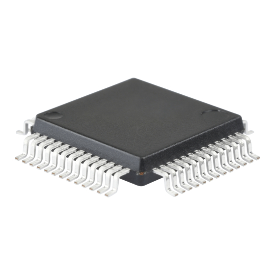
Page 56: Outline Dimensions
ADuC812 OUTLINE DIMENSIONS Dimensions shown in inches and (mm). 52-Lead Plastic Quad Flatpack (S-52) 0.094 (2.39) 0.557 (14.15) 0.084 (2.13) 0.537 (13.65) 0.037 (0.95) 0.026 (0.65) PIN 1 SEATING PLANE 0.398 (10.11) TOP VIEW (PINS DOWN) 0.390 (9.91) 0.012 (0.30) 0.006 (0.15) 0.008 (0.20) 0.006 (0.15)
Need help?
Do you have a question about the MicroConverter ADuC812 and is the answer not in the manual?
Questions and answers