Table of Contents
Advertisement
Quick Links
Introduction
The STM32L4R9I-EVAL board is designed as a complete demonstration and development
platform for the STMicroelectronics Arm
microcontroller with four I²C buses, three SPI and six USART ports, CAN port, two SAI
ports, 12-bit ADC, 12-bit DAC, internal 640-Kbyte SRAM and 2-Mbyte flash memory, two
Octo-SPI memory interfaces, touch-sensing capability, USB OTG FS port, LCD-TFT
controller, MIPI DSI
interface and JTAG debugging support.
The STM32L4R9I-EVAL, shown in
design for user application development before porting to the final product.
The full range of hardware features on the board helps the user to evaluate all the
peripherals (USB, USART, digital microphones, ADC and DAC, TFT LCD, MIPI DSI
display, LDR, SRAM, NOR flash memory device, Octo-SPI flash memory device, microSD™
card, sigma-delta modulators, CAN transceiver, EEPROM) and develop applications.
Extension headers allow easy connection of a daughterboard or wrapping board for a
specific application.
ST-LINK/V2-1 is integrated on the board, as the embedded in-circuit debugger and
programmer for the STM32 MCU and the USB Virtual COM port bridge.
July 2023
Evaluation board with STM32L4R9AI MCU
®
®
host controller, flexible memory controller (FMC), 8- to 14-bit camera
Figure
UM2248 Rev 5
®
Cortex
-M4 core-based STM32L4R9AI
3,
Figure
4, and
Figure
UM2248
User manual
5, is used as a reference
®
www.st.com
1/77
1
Advertisement
Table of Contents

Subscribe to Our Youtube Channel
Related Manuals for ST STM32L4R9I


Summary of Contents for ST STM32L4R9I
- Page 1 UM2248 User manual Evaluation board with STM32L4R9AI MCU Introduction The STM32L4R9I-EVAL board is designed as a complete demonstration and development ® ® platform for the STMicroelectronics Arm Cortex -M4 core-based STM32L4R9AI microcontroller with four I²C buses, three SPI and six USART ports, CAN port, two SAI...
-
Page 2: Table Of Contents
6.3.2 ST-LINK/V2-1 firmware upgrade ......19 ETM trace ..........19 Power supply . - Page 3 STM32L4R9I-EVAL used as a USB Device ..... . 27 6.10.2 STM32L4R9I-EVAL used as a USB Host ..... . . 28 6.10.3 Limitations in using the USB OTG FS port .
- Page 4 RGB TFT LCD connector (CN20) ......62 7.17 ST-LINK/V2-1 USB Micro-B connector (CN21) ....62 4/77...
- Page 5 Product marking ..........70 STM32L4R9I-EVAL product history ......71 Board revision history .
- Page 6 STM32L4R9I-EVAL I/O assignment ........
- Page 7 STM32L4R9I-EVAL hardware block diagram ........12...
-
Page 8: Features
Connector for ADC input and DAC output – JTAG/SWD connector – ETM trace debug connector – User interface through USB Virtual COM port – Embedded ST-LINK/V2-1 debug and flashing facility – TAG connector – STDC14 connector – Pmod™ connector –... -
Page 9: Ordering Information
UM2248 Ordering information • Flexible power supply options: power jack, ST-LINK/V2-1 USB connector, USB OTG FS connector, daughterboard • On-board ST-LINK/V2-1 debugger/programmer with USB re-enumeration capability: mass storage, Virtual COM port, and debug port • Microcontroller supply voltage: fixed 3.3 V or adjustable range of 1.71 to 3.6 V •... -
Page 10: Development Environment
STM32 flash memory for easy demonstration of the device peripherals in standalone mode. The latest versions of the demonstration source code and associated documentation can be downloaded from www.st.com. a. Windows is a trademark of the Microsoft group of companies. ®... -
Page 11: Conventions
In particular, pay attention to the following components: microSD™ card in its receptacle (CN8) MB1314 DSI display daughterboard in its connector (CN16) For product information related to the STM32L4R9AII6 microcontroller, visit the www.st.com website. UM2248 Rev 5 11/77... -
Page 12: Hardware Layout And Configuration
Figure 4, and Figure 5 are the three images showing the STM32L4R9I-EVAL main board top view with round DSI display, top view with TFT LCD, and bottom view. Figure 1. STM32L4R9I-EVAL hardware block diagram 3.3 V 1.8 V VDD ADJ... -
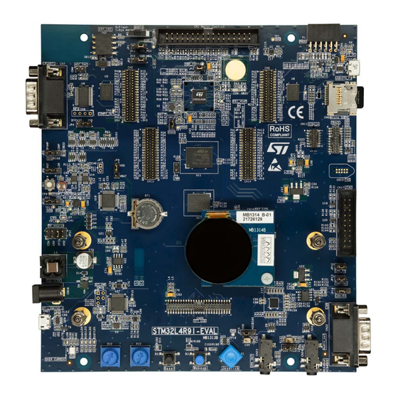
Page 13: Figure 2. Stm32L4R9I-Eval Main Board (Top Side)
UM2248 Hardware layout and configuration Figure 2. STM32L4R9I-EVAL main board (top side) UM2248 Rev 5 13/77... -
Page 14: Stm32L4R9I-Eval Main Board Views
Hardware layout and configuration UM2248 STM32L4R9I-EVAL main board views Figure 3. STM32L4R9I-EVAL board (top view) with MB1314 round DSI display daughterboard Picture is not contractual. 14/77 UM2248 Rev 5... -
Page 15: Figure 4. Stm32L4R9I-Eval Board (Top View) With Mb1315 Tft Lcd Daughterboard
UM2248 Hardware layout and configuration Figure 4. STM32L4R9I-EVAL board (top view) with MB1315 TFT LCD daughterboard Picture is not contractual. UM2248 Rev 5 15/77... -
Page 16: Figure 5. Stm32L4R9I-Eval Board (Bottom View)
Hardware layout and configuration UM2248 Figure 5. STM32L4R9I-EVAL board (bottom view) Picture is not contractual. 16/77 UM2248 Rev 5... -
Page 17: Mechanical Dimensions
UM2248 Hardware layout and configuration Mechanical dimensions Figure 6. MB1313 STM32L4R9I-EVAL main board UM2248 Rev 5 17/77... -
Page 18: St-Link/V2-1
UM2248 Figure 7. MB1314 DSI display daughterboard ST-LINK/V2-1 ST-LINK/V2-1 facility for debugging and flashing of the STM32L4R9AII6 is integrated on the STM32L4R9I-EVAL main board. Compared to the ST-LINK/V2 standalone tool available from STMicroelectronics, ST- LINK/V2-1 offers new features and drops some others. -
Page 19: Drivers
• SWIM interface The USB connector (CN21) can be used to power STM32L4R9I-EVAL regardless of the ST- LINK/V21 facility used for debugging or for flashing STM32L4R9AII6. This holds also when the ST-LINK/V2 standalone tool is connected to the CN12, CN17, CN11, or CN15 connector and used for debugging or flashing STM32L4R9AII6. -
Page 20: Power Supply
16 Mbits. Power supply The STM32L4R9I-EVAL main board must be powered from a 5 V DC power source. It incorporates a precise polymer Zener diode (Poly-Zen) protecting the main board from damage due to the wrong power supply. One of the following four 5 V DC power inputs is usable with an appropriate main board configuration: •... -
Page 21: Supplying The Main Board Through The St-Link/V2-1 Usb Port
100 mA. It is enough because only the ST-LINK/V2-1 part of STM32L4R9I-EVAL draws power at that time. If the SB33 solder bridge is OFF, the ST890 power switch (U22) is set in the OFF position, which isolates the remainder of STM32L4R9I-EVAL from the power source. -
Page 22: Table 5. Power-Supply-Related Jumpers Settings
USB port when the excessive current requirement from STM32L4R9I-EVAL is detected. This causes an operating failure to STM32L4R9I-EVAL. The host PC is not capable of supplying 300 mA (the enumeration fails) so ST-LINK/V2- 1 does not supply the remainder of STM32L4R9I-EVAL from its USB port V line. -
Page 23: Clock References
CN21 using a USB charger 1. On all ST-LINK/V2-1 boards, the target application is now able to run even if the ST-LINK/V2-1 is either not connected to a USB host, or powered through a USB charger or a nonenumerating USB Host). -
Page 24: Reset Sources
R65 must be OFF, in order not to disturb the clock reference or source on the daughterboard. Reset sources The reset signal of the STM32L4R9I-EVAL main board is active LOW. Sources of reset are listed below: • Reset button (B2) •... -
Page 25: Bootloader Limitations
The bootloader version is identified by reading the bootloader ID at the address 0x1FFF6FFE: the content is 0x91 for bootloader V9.1 and 0x92 for V9.2. The STM32L4R9AII6 part soldered on the STM32L4R9I-EVAL main board is marked with a date code corresponding to its date of manufacturing. STM32L4R9AII6 parts with a date code before or equal to week 37 of 2017 are installed with bootloader V9.1 affected by the... -
Page 26: Audio
There are two digital microphones on the STM32L4R9I-EVAL main board. 6.9.1 Digital microphones U30 and U31 on the STM32L4R9I-EVAL main board are MP34DT01TR MEMS digital omnidirectional microphones providing PDM (pulse density modulation) outputs. To share the same data line, their outputs are interlaced. The combined data output of the microphones is directly routed to STM32L4R9AII6 terminals, thanks to the integrated input digital filters. -
Page 27: Headphones Outputs
The resistor R23 must be left OFF to prevent STM32L4R9I-EVAL from sourcing the 5 V to the terminal, which would cause conflict with the 5 V sourced by the USB host. This might happen if the software of the MFX MCU controls MFX_GPIO6 such that, it enables the output of the power switch (U2). -
Page 28: Stm32L4R9I-Eval Used As A Usb Host
When a USB Device connection to the CN3 Micro-AB USB connector is detected, the STM32L4R9I-EVAL main board starts behaving like a USB Host. It sources 5 V on the V terminal of the Micro-AB USB connector (CN3) to power the USB device. For this to happen, the STM32L4R9AII6 sets the STMPS2151STR power switch (U2) to the ON state. -
Page 29: Operating Voltage
UM2248 Hardware layout and configuration 6.12.2 Operating voltage The supply voltage for the STM32L4R9I-EVAL microSD™ card operation must be within the range of 2.7 to 3.6 V. 6.13 Motor control The CN1 connector is designed to receive a motor-control (MC) module. - Page 30 Hardware layout and configuration UM2248 Table 10. Motor-control terminal and function assignment (continued) Motor-control STM32L4R9AII6 microcontroller connector (CN1) Alternate Terminal Port Board modifications for Terminal Function name name enabling motor control function PhaseA current- SB37 ON PhaseB ADC1_IN2 current+ R244 OFF PhaseB current- SB43 ON...
-
Page 31: Board Modifications To Enable Motor Control
UM2248 Hardware layout and configuration Table 10. Motor-control terminal and function assignment (continued) Motor-control STM32L4R9AII6 microcontroller connector (CN1) Alternate Terminal Port Board modifications for Terminal Function name name enabling motor control function SB17 ON Encoder B TIM4_CH2 ADC12_IN SB18 OFF R30 OFF or no daughterboard. -
Page 32: Figure 9. Pcb Top-Side Rework For Motor Control
Hardware layout and configuration UM2248 Figure 9. PCB top-side rework for motor control 32/77 UM2248 Rev 5... -
Page 33: Figure 10. Pcb Bottom-Side Rework For Motor Control
UM2248 Hardware layout and configuration Figure 10. PCB bottom-side rework for motor control UM2248 Rev 5 33/77... -
Page 34: Can
CAN_TX is used from the STM32L4R9AII6 terminal. 6.14.1 Limitations CAN operation is exclusive to the audio codec and MC operation. 6.14.2 Operating voltage The supply voltage for STM32L4R9I-EVAL CAN operation must be within the range of 3.0 to 3.6 V. 34/77 UM2248 Rev 5... -
Page 35: Extension Connectors (Cn5, Cn6, Cn13, And Cn14)
UM2248 Hardware layout and configuration 6.15 Extension connectors (CN5, CN6, CN13, and CN14) The CN5, CN6, CN13, and CN14 headers complement to give access to all GPIOs of the STM32L4R9AII6 microcontroller. In addition to GPIOs, the following signals and power supply lines are also routed on CN5, CN6, CN13, or CN14: •... -
Page 36: Physical Input Devices
Hardware layout and configuration UM2248 6.17 Physical input devices The STM32L4R9I-EVAL main board provides several input devices for physical human control, listed below: • Four-way joystick controller with select key (B1) • Wake-up/ tamper button (B3) • Reset button (B2) •... -
Page 37: Operational Amplifier And Comparator
Operational amplifier STM32L4R9AII6 provides two onboard operational amplifiers, one of which, OpAmp1, is made accessible on STM32L4R9I-EVAL. OpAmp1 has its inputs and its output routed to I/O ports PA0, PA1, and PA3, respectively. The noninverting input PA0 is accessible on terminal 1 of the jumper header (JP5). -
Page 38: Limitations
Hardware layout and configuration UM2248 I/O ports PB4 and PB5, respectively. The input is accessible on terminal 3 of the jumper header (JP5). On top of the possibility of routing either the potentiometer or LDR to PB4, an external source is connectable to it, using terminal 3 of JP5. The PB5 output of the comparator is accessible on test point TP6. -
Page 39: Sram Device
By default, the FMC_NWAIT signal is not routed to the RB port of the NOR flash memory device, and, to know its ready status, its status register is polled by the demo software installed in STM32L4R9I-EVAL. This is modifiable with configuration elements, as shown in Table... -
Page 40: Limitations
EEPROM M24128-DFDW6TP, a 128-Kbit I²C-bus EEPROM device (U3), is installed on the STM32L4R9I-EVAL main board. It is accessed with I²C-bus lines I2C2_SCL and I2C2_SDA of STM32L4R9AII6. It supports all I²C-bus modes with speeds up to 1 MHz. The base I²C- bus address is 0xA0. -
Page 41: Limitations
2.7 V to 3.6 V. 6.25 Octo-SPI DRAM device IS66WVH8M8BLL-100BLI, a 64-Mbit self-refresh dynamic RAM (DRAM) device with a HyperBus™ interface, is installed on the STM32L4R9I-EVAL main board, in the U5 position. It allows the evaluation of the STM32L4R9AII6 Octo-SPI interface. 6.25.1 Operating voltage The voltage of the Octo-SPI DRAM device IS66WVH8M8BLL-100BLI is in the range of 2.7 V to 3.6 V. -
Page 42: Touch-Sensing Button
6.26 Touch-sensing button The STM32L4R9I-EVAL main board supports a touch-sensing button based on either RC charging or the charge-transfer technique. The latter is enabled, by default. The touch-sensing button is connected to the PC6 port of STM32L4R9AII6 and the related charge capacitor is connected to PC7. -
Page 43: Limitations
MFX MCU The MFX MCU is used as MFX (multifunction expander) and IDD measurement. The MFX circuit on the STM32L4R9I-EVAL main board acts as an IO expander. The communication interface between MFX and STM32L4R9AII6 is the I2C2 bus. The signals... -
Page 44: Idd Measurement
(VDD_MCU line) does not exceed 3.3 V. This is because there are components on STM32L4R9I-EVAL supplied from 3.3 V that communicate with the MCU through I/O ports. Voltage exceeding 3.3 V on the MCU output port might inject current into 3.3 V-supplied peripheral I/Os and false the MCU current consumption measurement. -
Page 45: Mipi Dsi ® Display Connector
6.29 MIPI DSI display connector The CN16 connector is designed to connect a DSI display daughterboard. MB1314 daughterboard is available to mount on the STM32L4R9I-EVAL main board. Table 21 shows the assignment of CN16 and STM32L4R9AII6 terminals. Table 21. DSI display module connector (CN16) Pin No. -
Page 46: Limitations
TFT LCD (RGB and FMC mode) connector The 50-pin 1.27 mm-pitch female connector (CN20) is designed to connect the TFT LCD daughterboard, supporting RGB and FMC modes. MB1315 daughterboard is available to mount on the STM32L4R9I-EVAL main board with RGB mode. Table 22 shows the assignment of CN20 and STM32L4R9AII6 terminals. -
Page 47: Limitations
6.32 MB1314 DSI display daughterboard MB1314 is the DSI display daughterboard that is available to mount on the STM32L4R9I- EVAL main board via the CN1 connector. GVO IEG1120TB103GF-001 is selected for round LCD with one data lane, 390x390 resolution, 24 bpp with capacitive touch panel (FocalTech FT3x67 driver). - Page 48 Hardware layout and configuration UM2248 Table 24. Pin function description of the MB1314 daughterboard connector (CN1) Pin number Description Pin number Description DSI_D0_P DSI_D0_N BLVDD (5 V) BLVDD (5 V) BLGND BLGND 3.3 V I2C_SDA SWIRE I2C_SCL DSI_TE DSI_BL_CTRL DSI_RST Warning: Permanent image sticking might occur if AMOLED displays the same image for an extended time.
-
Page 49: Mb1315 Tft Lcd Daughterboard
MB1315 TFT LCD daughterboard MB1315 is the TFT LCD daughterboard supporting RGB mode, available to mount on the STM32L4R9I-EVAL main board via the CN1 connector. The 4.3” TFT LCD uses LCD RK043FN48H-CT672B with a capacitive touch panel, which only supports 3.3 V power and interface. So, a level shifter SN74LVC16T245DGGR is requested on the TFT RGB LCD daughterboard to support a wide power supply range. -
Page 50: Connectors
Connectors UM2248 Connectors Motor-control connector (CN1) Figure 11. Motor-control connector (CN1) top view MSv46051V1 Table 26. Motor-control connector (CN1) STM32L4R9AII6 CN1 pin CN1 pin STM32L4R9AII6 Description Description number number Emergency STOP PWM_1H PWM_1L PH13 PWM_2H PWM_2L PH14 PWM_3H PWM_3L PH15 BUS VOLTAGE CURRENT A CURRENT B... -
Page 51: External I 2 C Connector (Cn2)
UM2248 Connectors External I C connector (CN2) Figure 12. EXT_I2C connector (CN2) front view MS30715V2 Table 27. EXT_I2C connector (CN2) Pin number Description Pin number Description I2C1_SDA (PH5) I2C_SCL (PH4) EXT_RESET (MFX_GPIO8) USB OTG FS Micro-AB connector (CN3) Figure 13. USB OTG FS Micro-AB connector (CN3) front view Table 28. -
Page 52: Analog Input-Output Connector (Cn4)
Connectors UM2248 Analog input-output connector (CN4) Figure 14. Analog input-output connector (CN4) top view MSv46052V1 Table 29. Analog input-output connector (CN4) Pin number Description Pin number Description Analog input-output PA4 Extension connectors (CN5, CN6, CN13, and CN14) All GPIO signals from STM32L4R9AII6 are connected to extension connectors (CN5, CN6, CN13, and CN14). -
Page 53: Table 31. Daughterboard Extension Connector (Cn6)
UM2248 Connectors Table 30. Daughterboard extension connector (CN5) (continued) How to disconnect alternative functions to Description Alternative functions number use on the extension connector OCTOSPI2_IO3 U5 removed PH10 OCTOSPI2_IO5 U5 removed OCTOSPI2_NCS U5 removed PH12 OCTOSPI2_IO7 U5 removed OCTOSPI2_CLK U5 removed PG15 OCTOSPI2_DQS U5 removed... - Page 54 Connectors UM2248 Table 31. Daughterboard extension connector (CN6) (continued) How to disconnect alternative functions to Description Alternative functions number use on the extension connector PA12 USB OTG_DP No connection for CN3 PA11 USB OTG_DM No connection for CN3 LPUART1_RX U9 removed VBUS_FS, MC R203 and SB35 OFF SDIO1_D1, Trace_D0...
-
Page 55: Table 32. Daughterboard Extension Connector (Cn13)
UM2248 Connectors Table 31. Daughterboard extension connector (CN6) (continued) How to disconnect alternative functions to Description Alternative functions number use on the extension connector OCTOSPI1_IO3 U6 removed OCTOSPI1_NCS U6 removed Table 32. Daughterboard extension connector (CN13) How to disconnect alternative functions to Description Alternative functions number... -
Page 56: Table 33. Daughterboard Extension Connector (Cn14)
Connectors UM2248 Table 32. Daughterboard extension connector (CN13) (continued) How to disconnect alternative functions to Description Alternative functions number use on the extension connector FMC_A19 FMC_A22 Keep CN12 OFF FMC_A0 DFSDM, MC R242 and SB36 OFF SAI1, MC R244 and SB37 OFF FMC_A3 FMC_A14 FMC_A11... - Page 57 UM2248 Connectors Table 33. Daughterboard extension connector (CN14) (continued) How to disconnect alternative functions to Description Alternative functions number use on the extension connector FMC_D4 PE14 FMC_D11 PE15 FMC_D12 Do not use CN11, CN12, CN15, and CN17 for PA13 JTAG_TMS/SWDIO debug connector.
-
Page 58: Rs232 Connector (Cn7)
Connectors UM2248 RS232 connector (CN7) Figure 15. RS232 D-sub male connector (CN7) front view MS30720V1 Table 34. RS232 D-sub male connector (CN7) Pin number Description Description number RS232_RX (PG8) RS232_RTS (PB12) RS232_TX (PG7) RS232_CTS (PB13) microSD™ connector (CN8) Figure 16. microSD™ connector (CN8) top view 58/77 UM2248 Rev 5... -
Page 59: Mfx Programming Connector (Cn9)
UM2248 Connectors Table 35. microSD™ connector (CN8) Description Description number number SDIO_D2 (PC10) Vss/GND SDIO_D3 (PC11) SDIO_D0 (PC8) SDIO_CMD (PD2) SDIO_D1 (PC9) SDIO_CLK (PC12) MicroSDcard_detect (MFX GPIO15) MFX programming connector (CN9) The CN9 connector is used only for embedded MFX (multifunction expander) programming during board manufacturing. -
Page 60: Trace Debugging Connector (Cn12)
Connectors UM2248 7.10 Trace debugging connector (CN12) Figure 18. ETM trace debugging connector (CN12) top view MS30722V2 Table 37. Trace debugging connector (CN12) Description Description number number +3.3 V TMS/PA13 TCK/PA14 TDO/PB3 TDI/PA15 RESET# Trace_CLK/PE2 Trace_D0/PC9 or SWO/PB3 Trace_D1/PC10 or nTRST/PB4 Trace_D2/PE5 Trace_D3/PE6 7.11... -
Page 61: Mipi Dsi ® Display Connector (Cn16)
UM2248 Connectors ® 7.12 MIPI DSI display connector (CN16) ® A TFT color LCD with the MIPI DSI interface daughterboard is mounted on the CN16 connector. Refer to Section 6.29 for detail. 7.13 JTAG connector (CN17) Figure 19. JTAG/SWD debugging connector (CN17) top view MSv30722V2 Table 39. -
Page 62: Power Connector (Cn18)
Connectors UM2248 7.14 Power connector (CN18) The STM32L4R9I-EVAL main board is power-able with a DC 5 V power supply via the external power supply socket (CN18) shown in Figure 20. The central pin of CN18 must be positive. Figure 20. Power supply connector (CN18) front view... -
Page 63: Can D-Type Male Connector (Cn22)
UM2248 Connectors Table 40. USB Micro-B connector (CN21) front view Pin number Description Pin number Description (power) Shield 7.18 CAN D-type male connector (CN22) Figure 22. CAN D-type 9-pin male connector (CN22) front view MS30720V1 Table 41. CAN D-type 9-pin male connector (CN22) Pin number Description Pin number... -
Page 64: O Assignment
I/O assignment UM2248 I/O assignment Table 42. STM32L4R9I-EVAL I/O assignment Primary UFBGA RGB LCD with Motor-control Pin name Pinout assignment 169 DSI FMC mode connector DSI_CKN DSI_CKP DSI_D0N DSI_D0P DSI_D1N DSI_D1P VCAPDSI [L13] VDD12DSI [L13] VDD12DSI VSSDSI VSSDSI NRST NRST... - Page 65 UM2248 I/O assignment Table 42. STM32L4R9I-EVAL I/O assignment (continued) Primary UFBGA RGB LCD with Motor-control Pin name Pinout assignment 169 DSI FMC mode connector JTDO/TRACESWO NJTRST || COMP2_INP SAI1_SD_B || COMP2_OUT TSC_G2_IO3 || USART1_TX Encoder A TSC_G2_IO4 Encoder B SAI1_MCLK_A || CAN1_RX...
- Page 66 I/O assignment UM2248 Table 42. STM32L4R9I-EVAL I/O assignment (continued) Primary UFBGA RGB LCD with Motor-control Pin name Pinout assignment 169 DSI FMC mode connector FMC_NWE LCD_NWE FMC_NWAIT LCD_DE FMC_NE1 FMC_D13 LCD_R3 FMC_D14 LCD_R4 PD10 FMC_D15 LCD_R5 PD11 FMC_A16 LCD_R6 PD12...
- Page 67 UM2248 I/O assignment Table 42. STM32L4R9I-EVAL I/O assignment (continued) Primary UFBGA RGB LCD with Motor-control Pin name Pinout assignment 169 DSI FMC mode connector PF11 DSI_TE/LCD_DE PF12 FMC_A6 PF13 FMC_A7 LCD_B1 PF14 FMC_A8 LCD_G0 PF15 FMC_A9 LCD_G1 FMC_A10 FMC_A11 FMC_A12...
- Page 68 I/O assignment UM2248 Table 42. STM32L4R9I-EVAL I/O assignment (continued) Primary UFBGA RGB LCD with Motor-control Pin name Pinout assignment 169 DSI FMC mode connector SPI2_NSS SPI2_SCK SPI2_MISO SPI2_MOSI MC_EmergencyST Audio_INT OCTOSPIP2_NCS OCTOSPIP2_CLK OCTOSPIP2_IO2 PI10 OCTOSPIP2_IO1 PI11 OCTOSPIP2_IO0 VBAT VDDDSI VDDA...
- Page 69 UM2248 I/O assignment Table 42. STM32L4R9I-EVAL I/O assignment (continued) Primary UFBGA RGB LCD with Motor-control Pin name Pinout assignment 169 DSI FMC mode connector UM2248 Rev 5 69/77...
-
Page 70: Stm32L4R9I-Eval Product Information
Parts marked as "ES" or "E" are not yet qualified and therefore not approved for use in production. ST is not responsible for any consequences resulting from such use. In no event will ST be liable for the customer using any of these engineering samples in production. -
Page 71: Stm32L4R9I-Eval Product History
UM2248 STM32L4R9I-EVAL product information STM32L4R9I-EVAL product history Table 43. Product history Order Product Product change Product details Product limitations code identification description MCU: – STM32L4R9AII6 silicon revision “Y” MCU errata sheet: – STM32L4Rxxx and The main board does not STM32L4Sxxx device... - Page 72 STM32L4R9I-EVAL product information UM2248 Table 43. Product history (continued) Order Product Product change Product details Product limitations code identification description MCU: – STM32L4R9AII6 silicon revision “V” MCU errata sheet: – STM32L4Rxxx and The main board does not STM32L4Sxxx device support Octo-SPI...
-
Page 73: Board Revision History
UM2248 STM32L4R9I-EVAL product information Board revision history Table 44. Board revision history Board variant and Board change Board reference Board limitations revision description Initial revision – L3 changed into Murata BNX002-11 – T2, T3, T4, T5, T6, T7, T8 changed from... -
Page 74: Federal Communications Commission (Fcc) And Ised Canada Compliance Statements
Federal Communications Commission (FCC) and ISED Canada Compliance Statements UM2248 Federal Communications Commission (FCC) and ISED Canada Compliance Statements 10.1 FCC Compliance Statement Part 15.19 This device complies with part 15 of the FCC Rules. Operation is subject to the following two conditions: (1) this device may not cause harmful interference, and (2) this device must accept any interference received, including interference that may cause undesired operation. -
Page 75: Ised Compliance Statement
UM2248 Federal Communications Commission (FCC) and ISED Canada Compliance Statements 10.2 ISED Compliance Statement Compliance Statement ISED Canada ICES-003 Compliance Label: CAN ICES-3 (B) / NMB-3 (B). Déclaration de conformité Étiquette de conformité à la NMB-003 d'ISDE Canada: CAN ICES-3 (B) / NMB-3 (B). UM2248 Rev 5 75/77... -
Page 76: Revision History
Revision history Table 45. Document revision history Date Revision Changes 18-Aug-2017 Initial version Added: – STM32L4R9I-EVAL board bottom view in Figure 5 – Bootloader limitation in Chapter 9.8.1 – Warning on AMOLED display in Chapter 9.32 25-Oct-2017 Updated: – Cover views... - Page 77 ST products and/or to this document at any time without notice. Purchasers should obtain the latest relevant information on ST products before placing orders. ST products are sold pursuant to ST’s terms and conditions of sale in place at the time of order acknowledgment.
Need help?
Do you have a question about the STM32L4R9I and is the answer not in the manual?
Questions and answers