Table of Contents
Advertisement
Getting started with STM32L1xxx hardware development
1
Introduction
This application note is intended for system designers who require a hardware
implementation overview of the development board features such as the power supply, the
clock management, the reset control, the boot mode settings and the debug management. It
shows how to use STM32L1xxx product families and describes the minimum hardware
resources required to develop an STM32L1xxx application.
Detailed reference design schematics are also contained in this document with descriptions
of the main components, interfaces and modes.
June 2011
Doc ID 17496 Rev 5
AN3216
Application note
1/30
www.st.com
Advertisement
Table of Contents

Related Manuals for ST STM32L152-EVAL


Summary of Contents for ST STM32L152-EVAL
-
Page 1: Introduction
STM32L1xxx product families and describes the minimum hardware resources required to develop an STM32L1xxx application. Detailed reference design schematics are also contained in this document with descriptions of the main components, interfaces and modes. June 2011 Doc ID 17496 Rev 5 1/30 www.st.com... -
Page 2: Table Of Contents
Contents AN3216 Contents Introduction ..........1 Power supplies . - Page 3 AN3216 Contents Pinout and debug port pins ........20 5.3.1 SWJ debug port pins .
- Page 4 List of tables AN3216 List of tables Table 1. Boot modes............. 18 Table 2.
- Page 5 AN3216 List of figures List of figures Figure 1. Power supply overview ........... . . 6 Figure 2.
-
Page 6: Power Supplies
Power supplies AN3216 Power supplies Introduction The device requires a 2.0 V to 3.6 V operating voltage supply (V ), to be fully functional at full speed. This maximum frequency is only achieved when the digital power voltage V CORE is equal to 1.8 V (product voltage range 1). -
Page 7: Independent A/D Converter Supply And Reference Voltage
AN3216 Power supplies 2.1.1 Independent A/D converter supply and reference voltage To improve conversion accuracy, the ADC and the DAC have an independent power supply that can be filtered separately, and shielded from noise on the PCB. ● The ADC voltage supply input is available on a separate V ●... -
Page 8: Independent Lcd Supply
Power supplies AN3216 2.1.2 Independent LCD supply The V pin is provided to control the contrast of the glass LCD. This pin can be used in two ways: ● It can receive, from an external circuitry, the desired maximum voltage that is provided on the segment and common lines to the glass LCD by the microcontroller. -
Page 9: Power Supply Schemes
AN3216 Power supplies Power supply schemes The circuit is powered by a stabilized power supply, V ● The V pins must be connected to V with external decoupling capacitors; one single Tantalum or Ceramic capacitor (minimum 4.7 µF typical 10 µF) for the package + one 100 nF Ceramic capacitor for each V pin). -
Page 10: Figure 3. Power Supply Supervisors
Power supplies AN3216 Figure 3. Power supply supervisors D DA 100 mV hysteresis 100 mV hysteresis IT enabled PVD output BOR reset (NRST) BOR/PDR reset (NRST) POR/PDR reset (NRST) (Note 1) BOR always active (Note 2) BOR disabled by option byte (Note 3) POR/PDR (BOR not available) (Note 4) -
Page 11: Power-On Reset (Por)/Power-Down Reset (Pdr), Brownout Reset (Bor)
AN3216 Power supplies 2.3.1 Power-on reset (POR)/power-down reset (PDR), brownout reset (BOR) The monitoring voltage begins at 0.7 V. During power-on, for devices operating between 1.8 and 3.6 V, the BOR keeps the device under reset until the supply voltages (V and V ) come close to the lowest acceptable DDIO... -
Page 12: Brownout Reset (Bor)
Power supplies AN3216 Figure 5. PVD thresholds 100 mV PVD threshold hysteresis PVD output 2.3.3 Brownout reset (BOR) During power on, the brownout reset (BOR) keeps the device under reset until the supply voltage reaches the specified V threshold. For devices operating from 1.65 to 3.6 V, the BOR option is not available and the power supply is monitored by the POR/PDR. -
Page 13: System Reset
AN3216 Power supplies 2.3.4 System reset A system reset sets all registers to their reset values except for the RTC, backup registers and RCC control/status register, RCC_CSR. A system reset is generated when one of the following events occurs: A low level on the NRST pin (external reset) Window watchdog end-of-count condition (WWDG reset) Independent watchdog end-of-count condition (IWDG reset) A reset bit set by software (SWreset) -
Page 14: Clocks
Clocks AN3216 Clocks Four different clock sources can be used to drive the system clock (SYSCLK). They are: ● HSI ((high-speed internal) oscillator clock ● HSE (high-speed external) oscillator clock ● PLL clock ● MSI (multispeed internal) oscillator clock The MSI is used as a system clock source after startup from reset, wake-up from Stop or Standby low power modes. -
Page 15: Hse Osc Clock
AN3216 Clocks HSE OSC clock The high-speed external clock signal (HSE) can be generated from two possible clock sources: ● HSE user external clock (see Figure ● HSE external crystal/ceramic resonator (see Figure Figure 7. External clock Figure 8. Crystal/ceramic resonators Hardware configuration OSC_IN OSC_OUT... -
Page 16: Lse Osc Clock
5 to 6 R (resonator series resistance). To fine tune the R value refer to AN2867 (Oscillator design guide for ST microcontrollers). 3.3.1 External source (LSE bypass) In this mode, an external clock source must be provided. It must have a frequency of 32.768 kHz. -
Page 17: Clock Security System (Css)
AN3216 Clocks Clock security system (CSS) The clock security system can be activated by software. In this case, the clock detector is enabled after the HSE oscillator startup delay, and disabled when this oscillator is stopped. If a failure is detected on the HSE oscillator clock, this oscillator is automatically disabled and an interrupt is generated to inform the software about the failure (clock security system interrupt, CSSI), allowing the MCU to perform rescue operations. -
Page 18: Boot Configuration
Boot configuration AN3216 Boot configuration Boot mode selection In the STM32L1xxx, three different boot modes can be selected by means of the BOOT[1:0] pins as shown in Table Table 1. Boot modes BOOT mode selection pins Boot mode Aliasing BOOT1 BOOT0 Main Flash memory is selected as boot Main Flash memory... -
Page 19: Embedded Boot Loader Mode
The embedded boot loader is used to reprogram the Flash memory through one of the following interfaces: USART1 or USART2. This program is located in the system memory and is programmed by ST during production (see the STM32L Flash programming manual for further details). -
Page 20: Debug Management
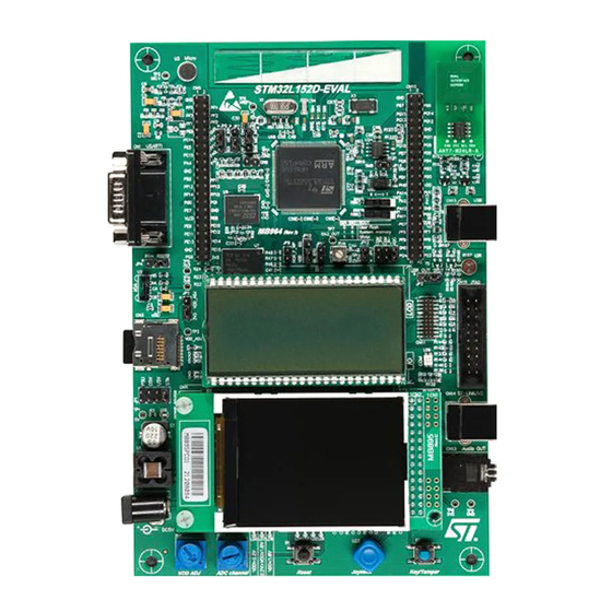
Figure 12 shows the connection of the host to a development board. The evaluation board (STM32L152-EVAL) embeds the debug tools (ST-LINK) so it can be directly connected to the PC through an USB cable. Figure 12. Host-to-board connection SWJ debug port (serial wire and JTAG) The STM32L1xxx core integrates the serial wire/JTAG debug port (SWJ-DP). -
Page 21: Swj Debug Port Pins
AN3216 Debug management 5.3.1 SWJ debug port pins Five pins are used as outputs for the SWJ-DP as alternate functions of general-purpose I/Os (GPIOs). These pins, shown in Table 2, are available on all packages. Table 2. Debug port pin assignment JTAG debug port SW debug port SWJ-DP pin name... -
Page 22: Internal Pull-Up And Pull-Down Resistors On Jtag Pins
Debug management AN3216 5.3.3 Internal pull-up and pull-down resistors on JTAG pins The JTAG input pins must not be floating since they are directly connected to flip-flops which control the debug mode features. Special care must be taken with the SWCLK/TCK pin that is directly connected to the clock of some of these flip-flops. -
Page 23: Recommendations
AN3216 Recommendations Recommendations Printed circuit board For technical reasons, it is best to use a multilayer printed circuit board (PCB) with a separate layer dedicated to ground (V ) and another dedicated to the V supply. This provides good decoupling and a good shielding effect. For many applications, economical reasons prohibit the use of this type of board. -
Page 24: Other Signals
Recommendations AN3216 Figure 14. Typical layout for V pair Via to V Via to V Cap. STM32L1xxx Other signals When designing an application, the EMC performance can be improved by closely studying the following: ● Signals for which a temporary disturbance affects the running process permanently (which is the case for interrupts and handshaking strobe signals but, not the case for LED commands). -
Page 25: Reference Design
AN3216 Reference design Reference design Description The reference design shown in Figure 15, is based on the STM32L152VB(T6) This reference design can be tailored to any STM32L1xxx device with a different package, using the pin correspondence given in Table 6: Reference connection for all packages. -
Page 26: Component References
Reference design AN3216 Component references Table 4. Mandatory components Id Components name Reference Quantity Comments 1 Microcontroller STM32L152VB(T6) 100-pin package Ceramic capacitors (decoupling 2 Capacitors 100 nF 3 ... 6 capacitors) 3 Capacitor 10 µF Ceramic capacitor (decoupling capacitor) Ceramic capacitor (LCD booster or 4 Capacitor 1 µF decoupling capacitor) -
Page 27: Figure 15. Stm32L152Vb(T6) Microcontroller Reference Schematic
AN3216 Reference design Figure 15. STM32L152VB(T6) microcontroller reference schematic Doc ID 17496 Rev 5 27/30... -
Page 28: Table 6. Reference Connection For All Packages
Reference design AN3216 Table 6. Reference connection for all packages Pin numbers for LQFP Pin numbers for BGA Pin numbers for packages packages VFQFPN package Pin name 100 pins 64 pins 48 pins 100 pins 64 pins 48 pins PH0-OSC_IN PH1- OSC_OUT PC15-... -
Page 29: Revision History
AN3216 Revision history Revision history Table 7. Document revision history Date Revision Changes 28-Jun-2010 Initial release Updated the following sections: Section 2.1: Introduction, Section 2.1.1: Independent A/D converter supply and reference voltage, Section 2.1.2: Independent LCD supply, Section 2.3.1: Power-on reset (POR)/power-down reset (PDR), brownout reset (BOR), and Section 2.3.4: System reset. - Page 30 No license, express or implied, by estoppel or otherwise, to any intellectual property rights is granted under this document. If any part of this document refers to any third party products or services it shall not be deemed a license grant by ST for the use of such third party products or services, or any intellectual property contained therein or considered as a warranty covering the use in any manner whatsoever of such third party products or services or any intellectual property contained therein.
Need help?
Do you have a question about the STM32L152-EVAL and is the answer not in the manual?
Questions and answers