Table of Contents
Advertisement
Quick Links
UM1878
User manual
Evaluation board with STM32L073VZ MCU
Introduction
The STM32L073Z-EVAL evaluation board is designed as a complete demonstration and
®
®
development platform for the STMicroelectronics Arm
Cortex
-M0+ core-based
2
STM32L073VZT6 microcontroller with three I
C buses, two SPI interfaces, four USART
interfaces, one UART interface, 12-bit ADC and DAC, LCD driver, up to 192-Kbyte Flash
memory, 20-Kbyte RAM, 6-Kbyte EEPROM, touch sensing, USB OTG FS, LCD controller,
SWD debugging support. This evaluation board can be used as reference design for user
application development but is not considered as a final application.
The full range of hardware features on the board help the user to evaluate all peripherals
(USB OTG FS, USART, 12-bit ADC and DAC, color TFT LCD, LCD glass, low-power UART,
IrDA, microSD™ card, touch sensing slider, pressure measurement, temperature
measurement, LC sensor metering) and develop his applications. The extension headers
offer the possibility to connect a daughterboard or a wrapping board for a specific
application.
An embedded ST-LINK/V2-1 debugger facilitates the software development and the
programming of the STM32L073VZT6 microcontroller.
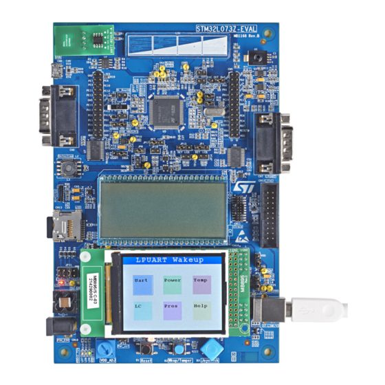
Figure 1. STM32L073Z-EVAL evaluation board
Picture is not contractual.
May 2018
UM1878 Rev 2
1/64
www.st.com
1
Advertisement
Table of Contents

Related Manuals for ST STM32L073Z-EVAL


Summary of Contents for ST STM32L073Z-EVAL
- Page 1 UM1878 User manual Evaluation board with STM32L073VZ MCU Introduction The STM32L073Z-EVAL evaluation board is designed as a complete demonstration and ® ® development platform for the STMicroelectronics Arm Cortex -M0+ core-based STM32L073VZT6 microcontroller with three I C buses, two SPI interfaces, four USART...
-
Page 2: Table Of Contents
Hardware layout and configuration ......10 Embedded ST-LINK/V2-1 ........11 7.1.1... - Page 3 UM1878 Contents 7.10.2 Operating voltage ......... 21 7.11 Virtual Com Port .
- Page 4 ST-LINK/V2-1 programming connector CN15 ..... 46 ST-LINK/V2-1 USB Type B connector CN17 ..... . 46 SWD connector CN12 .
- Page 5 UM1878 List of tables List of tables Table 1. Ordering information ............9 Table 2.
- Page 6 Figure 3. STM32L073Z-EVAL evaluation board (top view) ....... . 11 Figure 4.
-
Page 7: Features
192 Kbytes of Flash memory and 20 Kbytes of RAM in LQFP100 package • Four 5 V power supply options: power jack, ST-LINK USB connector, user USB FS connector, or daughterboard • Selectable MCU voltage: 3.3 V or adjustable from 1.7 V to 3.6 V •... -
Page 8: Product Marking
• on the targeted STM32 that is soldered on the board (for illustration of STM32 marking, refer to the section Package information in the STM32 datasheet at www.st.com). • next to the evaluation tool ordering part number, that is stuck or silkscreen printed on... -
Page 9: Demonstration Software
MCU, is preloaded in the STM32 Flash memory for easy demonstration of the device peripherals in standalone mode. The latest versions of the demonstration source code and associated documentation can be downloaded from www.st.com. Ordering information To order the STM32L073Z-EVAL Evaluation board, refer to Table Table 1. -
Page 10: Hardware Layout And Configuration
Hardware layout and configuration UM1878 Hardware layout and configuration STM32L073Z-EVAL evaluation board is designed around the STM32L073VZT6 (LQFP 100 package). The hardware block Figure 2: Hardware block diagram illustrates the connections between the STM32L073VZT6 and peripherals while Figure 3: STM32L073Z-EVAL... -
Page 11: Embedded St-Link/V2-1
UM1878 Hardware layout and configuration Figure 3. STM32L073Z-EVAL evaluation board (top view) Embedded ST-LINK/V2-1 The ST-LINK/V2-1 programming and debugging tool is integrated on the STM32L073Z-EVAL evaluation board. Compared to ST-LINK/V2 the changes are listed below. UM1878 Rev 2 11/64... -
Page 12: Drivers
Windows XP, 7, 8. In case the STM32L073Z-EVAL evaluation board is connected to the PC before the driver is installed, some STM32L073Z-EVAL interfaces may be declared as “Unknown” in the PC device manager. In this case the user must install the driver files, and update the driver of the connected device from the device manager. -
Page 13: Swd Connectors
JTAG are not available on the STM32L073VZT6 microcontroller. Power supply STM32L073Z-EVAL evaluation board is designed to be powered by a 5 V DC power supply and to be protected from wrong power plug-in event by PolyZen. It is possible to configure the evaluation board to use any of the following four power supply sources: •... -
Page 14: Table 2. Power Related Jumpers
Description JP11 is used to select one of the four possible power supply sources. To supply STM32L073Z-EVAL only from a 5 V power adapter connected to CN18 (PSU_E5V), set the jumper to E5V location, as following (Default setting): To supply STM32L073Z-EVAL only from the USB connector CN9 set the jumper to... - Page 15 Table 2. Power related jumpers (continued) Jumper Description To supply both STM32L073Z-EVAL and a daughterboard connected to extension connectors CN4 and CN5, (daughterboard should have its own power supply not connected), set jumpers to E5V and D5V locations, as following:...
-
Page 16: Adjustable Power Supply
JP13 If JP13 is connected, ST-LINK will never supply the evaluation board from ST-LINK USB. The red LED LD5 is on when the board STM32L073Z-EVAL is powered correctly by the 5 V. 7.3.1 Adjustable power supply As detailed above the STM32L073VZT6 microcontroller can be supplied by a variable voltage when pins 2 and 3 of JP12 are connected by a jumper. -
Page 17: Clock Source
PH1 is connected to pin 7 of extension connector CN5. In such SB23 closed case R342 must be removed to avoid disturbance due to the crystal. Reset sources The RESET signal of STM32L073Z-EVAL evaluation board is active low. UM1878 Rev 2 17/64... -
Page 18: Boot Option
Note (AN2606) details the bootloader mechanism and configurations. Table 5. Boot related switch Switch Description STM32L073Z-EVAL evaluation board boots from User Flash. BOOT0 pin is tied to “Low”. (default setting) STM32L073VZT6 boots from system Flash memory (nBOOT1 bit of FLASH_OPTR register is set high) or from RAM (nBOOT1 is set low). -
Page 19: Usb Fs
Section 7.3: Power supply for more details. • If V is supplied from USB (U5V voltage), STM32L073Z-EVAL is functional in all DD_USB the voltage range: 1.65 V to 3.6 V. SMBus temperature sensor A temperature sensor STLM75M2F is connected to I2C1 bus and to the SMBus of the microcontroller STM32L073VZT6. -
Page 20: Limitations
RS-232 USART2 and IrDA 7.9.1 RS-232 The evaluation board STM32L073Z-EVAL offers an RS-232 communication port at the DB9 male connector CN6. The signals RX, TX, RTS and CTS from USART2 of STM32L073VZT6 are available. Signals Bootloader_RESET and Bootloader_BOOT0 can be added on RS-232 connector CN6 for ISP support. -
Page 21: Limitations
7.11 Virtual Com Port RX and TX of USART4 are available in a USB Virtual Com Port managed by the ST- LINK/V2-1. The USB connector of ST-LINK/V2-1 is CN17. Virtual Com Port can be used over the whole operating voltage range of the microcontroller because level shifters are used. -
Page 22: Limitations
If V < 2.7 V the SPI clock should be 8 MHz maximum. 7.12.2 Operating voltage STM32L073Z-EVAL evaluation board Micro SD card is operating over whole range of V 1.65 V to 3.6 V. 7.13 Analog input ADC The analog input ADC_IN5 (port PA5) of the microcontroller STM32L073VZT6 is available at connector CN2. -
Page 23: Figure 6. Location Of Adc Input Connector Cn2
Figure 7. Provision for filter implementation As the port PA5 can be used also a DAC output, the STM32L073Z-EVAL evaluation board gives also provision to build an output filter structure by replacing R8 and C2 by appropriate values. -
Page 24: Operating Voltage
Hardware layout and configuration UM1878 7.13.1 Operating voltage ADC input is operational with V >1.8 V. 7.14 Analog output DAC The analog output DAC_OUT1 (port PA4) of microcontroller STM32L073VZT6 is available at connector CN3 located below the touch sensing slider as shown below. The left pin of CN3 is the connection of GND reference, and right pin is DAC output voltage. -
Page 25: Limitations
Figure 9. Provision for filter implementation As the port PA4 can be used also as ADC input IN4, the STM32L073Z-EVAL evaluation board gives also provision to build an input filter structure by replacing R28 and C15 by appropriate values. -
Page 26: Tft Lcd Display
Hardware layout and configuration UM1878 7.15 TFT LCD display The 2.4” color TFT LCD is connected to SPI1 port of STM32L073VZT6. The LCD TFT module is the MB895/S. Table 11. TFT LCD connector 2.4” TFT LCD connector CN16 Description Pin connection Description Pin connection PE10... -
Page 27: Input Devices
A LCD glass module daughterboard (MB979) is mounted in the connectors CN10 and CN14 of the STM32L073Z-EVAL evaluation board. It can be connected to the LCD driver pins of the STM32L073VZT6 or work as a set of jumpers to route the microcontroller pins for another usage, depending on the position: •... -
Page 28: Table 14. Lcd Glass Segments 21 To 28 Mapping Table
Hardware layout and configuration UM1878 Figure 10. LCD glass board in LCD position Figure 11. LCD glass board in IO position The custom LCD glass module used on MB979 daughterboard is XHO5002B. The signal mapping of each LCD segment is detailed in following table (rows are LCD_COMx, columns LCD_SEGy, with x comprised between 0 and 7, y from 0 to 39): Table 14. -
Page 29: Table 15. Lcd Glass Segments 0 And 29 To 39 Mapping Table
UM1878 Hardware layout and configuration Table 15. LCD glass segments 0 and 29 to 39 mapping table COM7 9g 13g 14g 15g 16g 17g COM6 9h 13h 14h 15h 16h 17h COM5 9i COM4 9j COM3 9d 13d 14d 15d 16d 17d COM2 9c COM0 9e 13e 14e 15e 16e 17e... -
Page 30: Table 18. Lcd Glass Related Jumpers And Solder Bridges
Table 18. LCD glass related jumpers and solder bridges Jumpers, solder Description bridges, resistors JP8 closed The LC network (L2 or L3, and C40) on STM32L073Z-EVAL is used for LC sensor metering. Nothing is connected to connector CN8. SB29, SB30 closed JP8,... -
Page 31: Limitations
LPTIM. A small board called Detection Accessory MB1199 is proposed with the evaluation board STM32L073Z-EVAL, to test the LC sensor metering quickly. The copper area to detect is 12 mm by 12 mm wide. UM1878 Rev 2... -
Page 32: Lc Sensor Metering Principle
Hardware layout and configuration UM1878 7.20.1 LC sensor metering principle Figure 13. Functional block diagram of LC sensor metering The port PD7 of the microcontroller STM32L073VZT6 is configured in GPIO output to deliver a high state. PD7 is in fact the signal called POWER_CONTROL. It is in charge to provide power supply to the resistor divider Ra, Rb and the follower amplifier based on an operational amplifier. -
Page 33: Lc Sensor Metering Description
LPTIM timer that is lower with metal presence than without. 7.20.2 LC sensor metering description The LC sensor metering of STM32L073Z-EVAL evaluation board follows closely the principle described above (see Figure 14). -
Page 34: Table 19. Solder Bridges And Jumpers For Lc Sensor Metering
Table 19. Solder bridges and jumpers for LC sensor metering Jumpers, solder bridges, Description resistors JP8 closed The LC network (L2 or L3, and C40) on STM32L073Z-EVAL is used for LC sensor metering. Nothing is connected to connector CN8. SB29, SB30 closed JP8, (default setting) -
Page 35: Limitations
UM1878 Hardware layout and configuration Table 19. Solder bridges and jumpers for LC sensor metering (continued) Jumpers, solder bridges, Description resistors JP1, JP15, JP17, JP2: 2,3 closed LC sensor metering is used, and is exclusive with LCD glass and DAC output. JP1, JP15, JP17 with pins 2 and 3 closed: ports PA7, PB4, PC0 are used for LC sensor metering signals: DET_COMP2_OUT, DET_COMP2_INP, JP14, JP16, JP18:... -
Page 36: Table 20. Sensor Differential Voltage
Hardware layout and configuration UM1878 Table 20. Sensor differential voltage Pressure Sensor differential voltage 0 HPa 0 mV 800 HPa 10.56 mV 1000 HPa 13.2mV 1200 HPa 15.84 mV As the proposed pressure measurement targets only barometric use, the sensor is used only in the range from 800 HPa to 1000 HPa, then the amplification is centered on this range. -
Page 37: Errors
15.84 mV +1.23V Finally, in STM32L073Z-EVAL evaluation board, the differential voltage is shifted by a V offset and changed in a single voltage by the last unity gain operational amplifier. The output of this amplifier, delivers the single output voltage to the ADC input PA0: Table 22. -
Page 38: Limitations
Operating voltage is fixed at: +3.3 V 7.22 Touch sensing slider The STM32L073Z-EVAL evaluation board supports a touch sensing slider based on either RC charging or charge transfer technology. The charge transfer technology is enabled by the default assembly. The touch sensing slider is connected to PB12, PB0, PA1 and the related charge capacitors are respectively connected to PB13, PB1 and PA2. -
Page 39: Limitations
Two 2.54 mm pitch headers CN4 and CN5 called “extension connectors” are intended to connect an external board to the STM32L073Z-EVAL evaluation board. Both connectors CN4 and CN5 give access to the GPIOs that are not accessible by the LCD glass connectors. -
Page 40: Idd Auto-Measurement
IDD auto-measurement In addition to the jumpers allowing to measure separately each power domain or the whole microcontroller consumption, the STM32L073Z-EVAL evaluation board offers also an automatic consumption measurement. The current of the microcontroller STM32L073VZT6 can be autonomously measured while it is in Run or Low power saving modes. -
Page 41: Analog Section Description
UM1878 Hardware layout and configuration Table 25. IDD auto-measurement related jumper settings Jumper Description JP10 2 and 3 closed (jumper in IDD position): STM32L073VZT6 is powered through IDD measurement circuit. (default setting) JP10 1 and 2 closed (jumper in position): JP10 IDD measurement circuit is bypassed, STM32L073VZT6 is powered directly. -
Page 42: Difference Amplifier
Hardware layout and configuration UM1878 The voltage drop across the selected shunt is amplified by a very high accuracy and zero-drift operational amplifier TSZ122. The voltage drop is connected to pins 3 and 5 of the operational amplifier TSZ122 U21. The digital section switches or not to a higher resistance shunt for a better measurement, depending on the measurement result obtained with one shunt. -
Page 43: Figure 19. Digital Section Schematic
UM1878 Hardware layout and configuration Figure 19. Digital section schematic Multi Function eXpander one capacitor close to each MFX pins: VDD, VDD_1, VDD_2, VDD_3 R166 BEAD MFX_IRQOUT C106 C116 PE6 can also be used to wake-up the MCU 100nF 100nF 100nF 100nF 100nF... -
Page 44: Connectors
RTS (PD4) TX (PD5) CTS/ Bootloader_RESET Power connector CN18 STM32L073Z-EVAL evaluation board can be powered from a DC 5 V power supply via the external power supply jack (CN18) shown in Figure 21: Power supply connector CN18. The central pin must be positive. -
Page 45: Lcd Glass Daughterboard Connectors Cn10 And Cn14
UM1878 Connectors LCD glass daughterboard connectors CN10 and CN14 Two 48-pins male headers CN10 and CN14 are used to connect with the LCD glass daughterboard (MB979). The space between these two connectors and the position of every LCD glass signals are defined as a standard, which allows to develop common daughterboards for several evaluations boards. -
Page 46: St-Link/V2-1 Programming Connector Cn15
It is not populated by default and not for end user. ST-LINK/V2-1 USB Type B connector CN17 The USB connector CN17 is used to connect embedded ST-LINK/V2-1 to PC for debugging of board. Figure 22. USB type B connector CN17 Table 28. -
Page 47: Swd Connector Cn12
UM1878 Connectors SWD connector CN12 Figure 23. Trace debugging connector CN12 (top view) Table 29. SWD debugging connector CN12 Pin number Description Pin number Description power power SWDIO PA13 SWCLK PA14 RESET# DBGRQ DBGACK Trace debugging connector CN11 Figure 24. Trace debugging connector CN11 (top view) UM1878 Rev 2 47/64... -
Page 48: Microsd Connector Cn3
Connectors UM1878 Table 30. Trace debugging connector CN11 Pin number Description Description number power SWDIO PA13 SWCLK PA14 Pin is removed RESET# MicroSD connector CN3 Figure 25. MicroSD connector CN3 Table 31. MicroSD connector CN3 Description Description number number MicroSD_CS (PD0) SPI_MISO (PE14) SPI_MOSI (PE15) +3V3... -
Page 49: Rf-Eeprom Daughterboard Connector Cn3
UM1878 Connectors RF-EEPROM daughterboard connector CN3 Figure 26. RF-EEPROM daughterboard connector CN3 (front view) Table 32. RF-EEPROM daughterboard connector CN3 Pin number Description Pin number Description I2C_SDA (PG13) I2C_SCL (PG14) EXT_RESET(PC6) UM1878 Rev 2 49/64... -
Page 50: Appendix A Electrical Schematics
Appendix A Electrical schematics Figure 27. STM32L073Z-EVAL U_Peripherals U_IDD_measurement Peripherals.SchDoc IDD_measurement.SchDoc MFX_MicroSD_detect JOY_SEL JOY_SEL JOY_DOWN JOY_DOWN JOY_LEFT JOY_LEFT JOY_RIGHT JOY_RIGHT JOY_UP JOY_UP I2C1_SCL MFX_I2C_SCL I2C1_SDA MFX_I2C_SDA MFX_IRQOUT RESET# MFX_WKUP U_MCU MCU.SchDoc MFX_WKUP MFX_IRQOUT I2C1_SDA I2C1_SCL EXT_RESET TempSensor_INT ADC_IN5 ADC_IN5 DAC_OUT1... -
Page 51: Figure 28. Mcu
SPI1_MOSI VLCD3 VDD_MCU [N/A] STM32L073VZT6 PH10 PH10 RESET C118 100nF 100nF BOOT0 LCDSEG[0..39] Bootloader_BOOT0_3V3 LCDSEG[0..39] BAT60JFILM LCDCOM[0..7] LCDCOM[0..7] BAT60JFILM Bootloader_RESET_3V3 DET_LPTIM_CH1 LCDSEG18 JP17 JP18 SB36 Open by default Title: Project: STM32L073Z-EVAL LCDSEG19 Size: Reference: MB1168 Revision: C-01 Date: 10/14/2015 Sheet:... -
Page 52: Figure 29. Lcd Glass External Connector
MCU PC15 SB26 Open by default PC14 SB27 PH10 PH10 Open by default BOOT0 BOOT0 SB23 Open by default SB25 Open by default LCDSEG[0..39] LCDSEG[0..39] LCDCOM[0..7] LCDCOM[0..7] Title: LCD_Glass_Ext_connector Project: STM32L073Z-EVAL Size: Reference: MB1168 Revision: C-01 Date: 10/14/2015 Sheet:... -
Page 53: Figure 30. Power
Closed by default SB21 Closed by default Closed by default SB19 Closed by default AGND is the local ground plane of pressure sensor circuitry (refer to ADC16b_Pressure schematic sheet) AGND Title: Power Project: STM32L073Z-EVAL Size: Reference: MB1168 Revision: C-01 Date: 10/14/2015 Sheet:... -
Page 54: Figure 31. Peripherals
[N/A] MT008-A EXT_RESET SSM-104-L-DH RFEEPROM module MB1020 A-02 is plugged in CN1 pins 1, 3, 5, 7 RFEEPROM & Extension Connector Title: Peripherals RF EEPROM MB1020 A-02 I2C address= 0xA6 Project: STM32L073Z-EVAL Size: Reference: MB1168 Revision: C-01 Date: 10/14/2015 Sheet:... -
Page 55: Figure 32. Tft Microsd
[N/A] BL_GND BL_GND R141 [N/A] SB40 TFT LCD Closed by default SB41 BEAD +3V3 C110 C111 Open by default SPI LCD 10uF R122 R139 100nF 100K 100K BEAD Title: TFT_MicroSD Project: STM32L073Z-EVAL Size: Reference: MB1168 Revision: C-01 Date: 10/14/2015 Sheet:... - Page 56 LPUART_RX_3V3 R1OUT R1IN R2OUT R2IN R3OUT R3IN PD11 LPUART_CTS_3V3 R4OUT R4IN R5OUT R5IN +3V3 nSHDN ST3241EBPR +3V3 100nF 100nF LPUART_TX VCCA VCCB PD12 LPUART_RTS_3V3 LPUART_RTS SN74LVC2T45DCUT 100K 100K Title: USART_LPUART Project: STM32L073Z-EVAL Size: Reference: MB1168 Revision: C-01 Date: 10/14/2015 Sheet:...
-
Page 57: Figure 34. Pressure Sensor
- AGND local ground plane is connected to GND by default using solder bridges SB1, SB2, SB3, SB19, SB20, SB21 or by a ferrite bead L1. (refer to Power sheet) - VDD_ANA is distributed in star scheme Title: ADC16b_Pressure Project: STM32L073Z-EVAL Size: Reference: MB1168 Revision:... -
Page 58: Figure 35. Lc Sensor Metering
Note *: Sensor inductors L2 or L3 are exclusive. Using a double PCB footprint. Open by default 100nF 330K TSV911ILT SB33 Vcc+ Vcc- Open by default [N/A] 330K Title: LC Detection Project: STM32L073Z-EVAL Size: Reference: MB1168 Revision: C-01 Date: 10/14/2015 Sheet:... -
Page 59: Figure 36. Idd Measurement
1K [0.1%] 100nF TSZ122IST Note *: two footprints superimposed allows to Current populate also with SO-8 package P MOS transistors: direction bypass STS7P2UH7, STS9P2UH7. JP10 VDD_MCU to MCU Title: IDD_measurement Project: STM32L073Z-EVAL Size: Reference: MB1168 Revision: C-01 Date: 10/14/2015 Sheet:... -
Page 60: Figure 37. Swd, Touch, Usb
47nF 47nF 4 buttons touch sensing slider I/O1 I/O1 100nF Vbus I/O2 I/O2 VBUS PA11 MICROB_N USBLC6-2P6 (optional) USB_DM PA12 MICROB_P USB_DP Shield Shield Shield 100K Shield 1050170001 Title: SWD_Touch_USB.SchDoc Project: STM32L073Z-EVAL Size: Reference: MB1168 Revision: C-01 Date: 2/4/2016 Sheet:... -
Page 61: Figure 38. St-Link/V2-1
Figure 38. ST-LINK/V2-1 output current limitation : 600mA LD3985M33R +3V3_STLINK BAT60JFILM Vout R168 R173 BAT60JFILM BYPASS BAT60JFILM BAT60JFILM JP13 +3V3_STLINK +3V3_STLINK VUSB_STLINK BAT60JFILM C103 C107 C115 R175 100nF 100nF 100nF 100nF USB_RENUMn 100K +3V3_STLINK STM_JTCK_SWCLK VUSB_STLINK U5V_STLINK STLINK 100nF 100nF... -
Page 62: Appendix B Mechanical Dimensions
Mechanical dimensions UM1878 Appendix B Mechanical dimensions Figure 39. Mechanical dimensions 62/64 UM1878 Rev 2... -
Page 63: Revision History
UM1878 Revision history Revision history Table 33. Document revision history Date Revision Changes 16-Feb-2016 Initial version. Added Chapter 3: System requirements Chapter 4: Development toolchains. 25-May-2018 Updated Chapter 1: Features, Chapter 2: Product marking, Chapter 5: Demonstration software, and Chapter 6: Ordering information. - Page 64 ST products and/or to this document at any time without notice. Purchasers should obtain the latest relevant information on ST products before placing orders. ST products are sold pursuant to ST’s terms and conditions of sale in place at the time of order acknowledgement.
Need help?
Do you have a question about the STM32L073Z-EVAL and is the answer not in the manual?
Questions and answers