Table of Contents
Advertisement
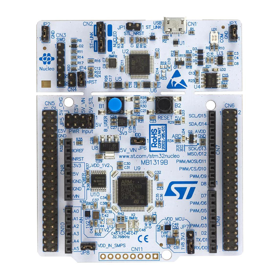
Figure 1. Nucleo-64-P board (top view)
Pictures are not contractual.
August 2018
Arrow.com.
Downloaded from
Introduction
The STM32 Nucleo-64-P boards (NUCLEO-L412RB-P, NUCLEO-L433RC-P and
NUCLEO-L452RE-P) provide an affordable and flexible way for users to try out new
concepts and build prototypes with the STM32 microcontroller and the external SMPS
(switched mode power supply), which provides various combinations of performance, power
consumption and features.
™
Arduino
Uno V3 connectivity and ST morpho headers provide an easy means of
expanding the functionality of the Nucleo open development platform with a wide choice of
specialized shields.
The STM32 Nucleo-64-P boards do not require any separate probe, as they integrate the
ST-LINK/V2-1 debugger/programmer. The STM32 Nucleo-64-P boards come with the
comprehensive free STM32 software libraries and examples that are available with the
STM32Cube package.
STM32 Nucleo-64-P boards
Figure 2. Nucleo-64-P board (bottom view)
UM2206 Rev 3
UM2206
User manual
1/55
www.st.com
1
Advertisement
Table of Contents

Related Manuals for ST STM32 Nucleo-64-P


Summary of Contents for ST STM32 Nucleo-64-P
-
Page 1: Figure 1. Nucleo-64-P Board (Top View)
Nucleo open development platform with a wide choice of specialized shields. The STM32 Nucleo-64-P boards do not require any separate probe, as they integrate the ST-LINK/V2-1 debugger/programmer. The STM32 Nucleo-64-P boards come with the comprehensive free STM32 software libraries and examples that are available with the STM32Cube package. -
Page 2: Table Of Contents
Embedded ST-LINK/V2-1 ........14... - Page 3 Arduino Uno V3 connectors ........34 10.3 ST morpho connectors CN5 and CN6 ......37 10.4 External power connector .
- Page 4 ST-LINK jumper configuration ........
- Page 5 STM32 Nucleo-64-P board bottom layout ........
-
Page 6: Features
Any consequences deriving from such usage will not be at ST charge. In no event, ST will be liable for any customer usage of these engineering sample tools as reference design or in production. -
Page 7: Ordering Information
SBx connections closed by 0 ohm resistor Solder bridge SBx OFF SBx connections left open In this document the references for all information that is common to all sale types, are “STM32 Nucleo-64-P board” and “STM32 Nucleo-64-P boards”. UM2206 Rev 3 7/55 Arrow.com. -
Page 8: System Requirements
The demonstration software, included in the STM32Cube MCU Package, is preloaded in the STM32 Flash memory for easy demonstration of the device peripherals in standalone mode. The latest versions of the demonstration source code and associated documentation can be downloaded from the www.st.com/stm32nucleo webpage. ® a. macOS is a trademark of Apple Inc.\nregistered in the U.S. -
Page 9: Quick Start
UM2206 Quick start Quick start This section describes how to start a development quickly using the STM32 Nucleo-64-P board. Before installing and using the product, accept the Evaluation Product License Agreement from the www.st.com/epla webpage. Getting started The STM32 Nucleo-64-P board is a low-cost and easy-to-use development kit to quickly evaluate and start a development with an STM32 microcontroller in QFP64 package. -
Page 10: Hardware Layout And Configuration
Hardware layout and configuration UM2206 Hardware layout and configuration The STM32 Nucleo-64-P board is designed around the STM32 microcontrollers in a 64-pins LQFP package. Figure 3 illustrates the connection between the STM32 and the peripherals (ST-LINK/V2-1, push-buttons, LEDs, Arduino Uno V3 connector and ST morpho connectors). -
Page 11: Stm32 Nucleo-64-P Board Layout
UM2206 Hardware layout and configuration STM32 Nucleo-64-P board layout Figure 4. STM32 Nucleo-64-P board top layout ST-LINK RST: JP1 USB_STLINK: CN1 ST-LINK debugger: COM LED: LD1 SWD: CN3 STLINK_3V3: U3 nRST: JP4 ST-LINK STM32: U2 UART VPN: CN4 STLINK_5V_SW: U4... -
Page 12: Figure 5. Stm32 Nucleo-64-P Board Bottom Layout
Hardware layout and configuration UM2206 Figure 5. STM32 Nucleo-64-P board bottom layout 12/55 UM2206 Rev 3 Arrow.com. Arrow.com. Arrow.com. Arrow.com. Arrow.com. Arrow.com. Arrow.com. Arrow.com. Arrow.com. Arrow.com. Arrow.com. Arrow.com. Downloaded from Downloaded from Downloaded from Downloaded from Downloaded from Downloaded from... -
Page 13: Stm32 Nucleo-64-P Board Mechanical Drawing
Figure 6. STM32 Nucleo-64 -P board mechanical drawing 9.2.1 Default board configuration By default the STM32 Nucleo-64-P board is delivered with the external SMPS 1.1 V enabled and V @3.3 V. It is possible to set the board for V @1.8 V. -
Page 14: Cuttable Pcb
An STM32 Nucleo-64-P board is divided into two parts: ST-LINK and target STM32. The ST-LINK part of the PCB can be cut out to reduce the board size. In this case the remaining target STM32 part can only be powered by V , E5V and 3.3 V on the ST morpho connector... -
Page 15: Drivers
In case the STM32 Nucleo-64-P board is connected to the PC before installing the driver, the PC device manager may report some Nucleo interfaces as “Unknown”. To recover from this situation, after installing the dedicated driver, the association of “Unknown” USB devices found on the STM32 Nucleo-64-P board to this dedicated driver, must be updated in the device manager manually. -
Page 16: Using The St-Link/V2-1 To Program/Debug The Stm32
9.4.4 Using the ST-LINK/V2-1 to program/debug an external STM32 application. It is very easy to use the ST-LINK/V2-1 to program the STM32 on an external application. Simply remove the two jumpers from CN2, as shown in Figure 9, and connect the... -
Page 17: Table 6. Debug Connector Swd
UM2206 Hardware layout and configuration Figure 9. ST-LINK debugger: jumper configuration for external MCU ST-LINK jumper OFF: CN2 [1-2] and [3-4] SWD connector: CN3 Table 6. Debug connector SWD Connector Pin name Signal name STM32 pin Function number VDD_TARGET: from application... -
Page 18: Power Supply And Power Selection
Power supply and power selection 9.5.1 External Power supply input The STM32 Nucleo-64-P board is designed to be powered by several DC power supply. It is possible to supply the STM32 Nucleo-64-P board with any of the following sources: •... -
Page 19: Figure 10. Jp5[1-2]: 5V_Stl Power Source
PC only provides 100 mA to the board at that time. During the USB enumeration, STM32 Nucleo-64-P board requires 500 mA of current to the host PC. If the host is able to provide the required power, the enumeration ends by a “SetConfiguration” command and then, the power transistor ST890 is switched ON, the green LED LD3 is turned ON, thus the STM32 Nucleo-64-P board and its shield request no more than 500 mA current. -
Page 20: Figure 11. Jp5[3-4]: 5V_Vin Power Source
CN8 pin 8 CN5 pin 24 E5V is the DC power coming from external (5V DC power from ST morpho connector CN5 pin 6). In this case JP5 jumper should be on pins 5 and 6 to select E5V power source on silkscreen of JP5. -
Page 21: Figure 12. Jp5[5-6]: E5V Power Source
5V_USB_CHARGER power source on silkscreen of JP5, the jumper of JP5 should be on pins 7 and 8. In this case, if the STM32 Nucleo-64-P board is powered by an external USB charger the debug is not available. If the PC is connected instead of the charger, the limitation is no more effective, in this case the PC could be damaged. -
Page 22: Table 8. Sb9 Configurations
Solder bridge SB9 can be used to bypass the USB power protection ST890. (This is not an ST recommended setting). SB9 can be set in case the board is powered by the USB of the PC and maximum current consumption on 5V_STLINK does not exceed 100 mA (including extension board or Arduino shield power consumption). -
Page 23: External Power Supply Output
5 V: the 5 V (CN8 pin 5 or CN5 pin 18) can be used as output power supply for an Arduino shield or an extension board, when the STM32 Nucleo-64-P board is powered by USB, V or E5V. In this case the maximum current allowed is showed in Table 3.3 V: on CN8 pin 4 or CN5 pin 16 can be also used as power supply output. -
Page 24: Programming/Debugging When The Power Supply Is Not From St-Link (5V_St_Link)
LSE which is the 32.768 KHz crystal for the STM32 embedded RTC • MCO which is the 8 MHz clock from the ST-LINK MCU for the STM32 microcontroller • HSE which is the 8 MHz oscillator for the STM32 microcontroller. This clock is not implemented on the STM32 Nucleo-64-P board. -
Page 25: Osc Clock Supply
There are four ways to configure the pins corresponding to the external-high-speed clock (HSE): MCO from ST-LINK (Default: not connected): MCO output of ST-LINK MCU is used as an input clock. This frequency cannot be changed, it is fixed at 8 MHz and connected to PH0 OSC_IN of the STM32 microcontroller. -
Page 26: Reset Sources
Hardware layout and configuration UM2206 Reset sources The reset signal of the STM32 Nucleo-64-P board is active low and the reset sources include: • Reset button B2 • Embedded ST-LINK/V2-1 • Arduino Uno V3 connector from CN8 pin 3 •... -
Page 27: Push Buttons
E5V, V or in USB_CHARGER mode. LD3: 5V_PWR: this green LED is ON when the STM32 Nucleo-64-P board is powered by a 5 V source. LD4 USER: this green LED is a user LED connected to Arduino signal D13 corresponding to STM32 I/O PB13. -
Page 28: Jumper Configuration
Used to reset ST-LINK MCU STLK_RST Normal use JP2/JP3 GND probe ST-LINK able to reset STM32 T_NRST ST-LINK not able to reset STM32 ON [1-2] 5 V from ST-LINK ON [3-4] 5 V from V 7-12 V 5 V Power selection... -
Page 29: Table 12. Solder Bridge Configurations And Settings
SWO not connected through level shifter SWO level SB10 SWO connected through level shifter to target MCU shifter by-pass for 1.8 V I/O configuration SWO_MCU connected between ST-LINK and target STM32 SWO_MCU SB11 SWO_MCU not connected between ST-LINK and target STM32... - Page 30 DD_1V2 SB30 / SB46 powered directly by U11/U12. Switch U10 DD_1V2 is not used (not recommended, see AN4978 on the U11/U12 www.st.com website) SMPS out powered directly by U11/U12. Switch U10 1.1 V DD_1V2 is not used. (not recommended, see AN4978 on the www.st.com...
- Page 31 HSE provided by External HSE CLK X2 SB67/SB69 HSE NOT provided by External HSE CLK X2 HSE CLK PH1 connected to ST morpho connector I/O usage selection SB68 PH1 NOT connected to ST morpho connector PH0 connected to ST morpho connector...
- Page 32 SB44, SB45, SB47, SB48, SB49, SB52, SB53, SB54, SB55, SB57, SB58, SB59, SB63, are linked to the STM32 configuration. Do not modify them. All STM32 Nucleo-64-P boards are delivered with solder bridges configured according to the target STM32 supported. 32/55 UM2206 Rev 3 Arrow.com.
-
Page 33: Connectors
CN11: External SMPS connector 10.1 USB Micro-B connector CN1 The USB connector CN1 is used to connect the embedded ST-LINK/V2-1 to the PC for programming and debugging the STM32 Nucleo-64-P board microcontroller. Figure 14. USB Micro-B connector CN1 (front view) -
Page 34: Arduino Uno V3 Connectors
15) are female connectors compatible with Arduino standard. Most shields designed for Arduino can fit to the STM32 Nucleo-64-P board. The Arduino connectors on STM32 Nucleo-64-P board support the Arduino Uno V3. Figure 15. Arduino connectors Arduino_PWR: CN8 Arduino_D[8..15]: CN7 Arduino_A[0..5]: CN10... -
Page 35: Table 14. Arduino Connector Pinout
UM2206 Connectors Figure 16. Arduino connector pinout NUCLEO_L4xxRx-P PC10 PC11 PC12 AVDD AVDD BOOT0 5V-STLINK PB13 IOREF IOREF PA10 PB14 PB12 NRST NRST PB15 PA13 PB11 PA11 PA14 PC13 PC14 PB10 PC15 PA15 AGND VBAT PA12 PA2/PA9 PA3/PA10 CN10 Arduino orpho Note: Arduino Uno V3 D0 and D1 signals are connected by default on USART1 (MCU I/O PA9... - Page 36 Connectors UM2206 Table 14. Arduino connector pinout (continued) Connector Pin number Pin name Signal name STM32 pin Function ADC1_IN5 ADC1_IN6 ADC1_IN4 ADC1_IN3 CN10 ADC1_IN2/I2C3_ ADC1_IN1/I2C3_ SCL/D15 ARD_D15 I2C1_SCL SDA/D14 ARD_D14 I2C1_SDA AVDD VREF VREF Ground SCK/D13 ARD_D13 PB13 SPI2_SCK MISO/D12 ARD_D12 PB14 SPI2_MISO...
-
Page 37: St Morpho Connectors Cn5 And Cn6
UM2206 Connectors 10.3 ST morpho connectors CN5 and CN6 The ST morpho connectors CN5 and CN6 are male pin headers accessible on both sides of the STM32 Nucleo-64-P board (see Figure 17). All signals and power pins, except 1.2 V of the STM32, are available on the ST morpho connectors. These DD_CORE connectors can also be probed by an oscilloscope, logical analyzer or voltmeter. -
Page 38: External Power Connector
Connectors UM2206 Figure 18. ST morpho connector pinout NUCLEO_L4xxRx-P PC10 PC11 PC12 AVDD AVDD BOOT0 5V-STLINK PB13 IOREF PA10 IOREF PB14 PB12 NRST NRST PB15 PA13 PB11 PA11 PA14 PC13 PC14 PB10 PC15 PA15 AGND VBAT PA12 PA2/PA9 PA3/PA10 CN10... -
Page 39: Table 15. External Power Connector Pinout
UM2206 Connectors Figure 19. External power connector The related pinout for external power connector is listed in Table Table 15. External power connector pinout Connector Signal name STM32 pin Function number @ 3.3 V supply MCU Core PWR 1.2 V/1.1 V OUTCORE DD_1V2 : 1.8 V / 3.3 V... -
Page 40: I/O Assignment
NUCLEO-L412RB-P, NUCLEO-L433RC-P and NUCLEO-L452RE-P I/O assignment UM2206 Appendix A NUCLEO-L412RB-P, NUCLEO-L433RC-P and NUCLEO-L452RE-P I/O assignment Table 16. NUCLEO-L412RB-P, NUCLEO-L433RC-P and NUCLEO-L452RE-P I/O assignment Pin name Signal or label Main feature / optional feature (SB) PWR V PC13 PC13 User Button / I/O PC14-OSC32_IN OSC32_IN / PC14 LSE CLK / I/O... - Page 41 UM2206 NUCLEO-L412RB-P, NUCLEO-L433RC-P and NUCLEO-L452RE-P I/O assignment Table 16. NUCLEO-L412RB-P, NUCLEO-L433RC-P and NUCLEO-L452RE-P I/O assignment (continued) Pin name Signal or label Main feature / optional feature (SB) PWR GND PWR V 1.8 V / 3.3 V DD_MCU DD_MCU PB12 PB12 PB13 PB13 ARD_D13 - SPI2_SCK / LED / IO...
- Page 42 NUCLEO-L412RB-P, NUCLEO-L433RC-P and NUCLEO-L452RE-P I/O assignment UM2206 Table 16. NUCLEO-L412RB-P, NUCLEO-L433RC-P and NUCLEO-L452RE-P I/O assignment (continued) Pin name Signal or label Main feature / optional feature (SB) PWR GND PWR V 1.8 V / 3.3 V DD_MCU DD_MCU 42/55 UM2206 Rev 3 Arrow.com.
-
Page 43: Appendix B Electrical Schematics
UM2206 Electrical schematics Appendix B Electrical schematics This section provides the design schematics for the STM32 Nucleo-64-P board features: • MB1319: – Top and Power (see Figure – STM32 I/Os (see Figure – STM32 Power (see Figure – Arduino extension connectors (see Figure –... -
Page 44: Figure 20. Top And Power
Electrical schematics UM2206 44/55 UM2206 Rev 3 Arrow.com. Arrow.com. Arrow.com. Arrow.com. Arrow.com. Arrow.com. Arrow.com. Arrow.com. Arrow.com. Arrow.com. Arrow.com. Arrow.com. Arrow.com. Arrow.com. Arrow.com. Arrow.com. Arrow.com. Arrow.com. Arrow.com. Arrow.com. Arrow.com. Arrow.com. Arrow.com. Arrow.com. Arrow.com. Arrow.com. Arrow.com. Arrow.com. Arrow.com. Arrow.com. Arrow.com. Arrow.com. Arrow.com. Arrow.com. -
Page 45: Figure 21. Stm32 I/Os
UM2206 Electrical schematics UM2206 Rev 3 45/55 Arrow.com. Arrow.com. Arrow.com. Arrow.com. Arrow.com. Arrow.com. Arrow.com. Arrow.com. Arrow.com. Arrow.com. Arrow.com. Arrow.com. Arrow.com. Arrow.com. Arrow.com. Arrow.com. Arrow.com. Arrow.com. Arrow.com. Arrow.com. Arrow.com. Arrow.com. Arrow.com. Arrow.com. Arrow.com. Arrow.com. Arrow.com. Arrow.com. Arrow.com. Arrow.com. Arrow.com. Arrow.com. Arrow.com. Arrow.com. -
Page 46: Figure 22. Stm32 Power
Electrical schematics UM2206 46/55 UM2206 Rev 3 Arrow.com. Arrow.com. Arrow.com. Arrow.com. Arrow.com. Arrow.com. Arrow.com. Arrow.com. Arrow.com. Arrow.com. Arrow.com. Arrow.com. Arrow.com. Arrow.com. Arrow.com. Arrow.com. Arrow.com. Arrow.com. Arrow.com. Arrow.com. Arrow.com. Arrow.com. Arrow.com. Arrow.com. Arrow.com. Arrow.com. Arrow.com. Arrow.com. Arrow.com. Arrow.com. Arrow.com. Arrow.com. Arrow.com. Arrow.com. -
Page 47: Figure 23. Arduino Extension Connectors
UM2206 Electrical schematics UM2206 Rev 3 47/55 Arrow.com. Arrow.com. Arrow.com. Arrow.com. Arrow.com. Arrow.com. Arrow.com. Arrow.com. Arrow.com. Arrow.com. Arrow.com. Arrow.com. Arrow.com. Arrow.com. Arrow.com. Arrow.com. Arrow.com. Arrow.com. Arrow.com. Arrow.com. Arrow.com. Arrow.com. Arrow.com. Arrow.com. Arrow.com. Arrow.com. Arrow.com. Arrow.com. Arrow.com. Arrow.com. Arrow.com. Arrow.com. Arrow.com. Arrow.com. -
Page 48: Figure 24. Main Power 5 V, 3.3 V
Electrical schematics UM2206 48/55 UM2206 Rev 3 Arrow.com. Arrow.com. Arrow.com. Arrow.com. Arrow.com. Arrow.com. Arrow.com. Arrow.com. Arrow.com. Arrow.com. Arrow.com. Arrow.com. Arrow.com. Arrow.com. Arrow.com. Arrow.com. Arrow.com. Arrow.com. Arrow.com. Arrow.com. Arrow.com. Arrow.com. Arrow.com. Arrow.com. Arrow.com. Arrow.com. Arrow.com. Arrow.com. Arrow.com. Arrow.com. Arrow.com. Arrow.com. Arrow.com. Arrow.com. -
Page 49: Figure 25. Stm32 Power Smps
UM2206 Electrical schematics VOUTCORE VOUTVDD SMPS_V1 SMPS_EN SMPS_SW SMPS_PG UM2206 Rev 3 49/55 Arrow.com. Arrow.com. Arrow.com. Arrow.com. Arrow.com. Arrow.com. Arrow.com. Arrow.com. Arrow.com. Arrow.com. Arrow.com. Arrow.com. Arrow.com. Arrow.com. Arrow.com. Arrow.com. Arrow.com. Arrow.com. Arrow.com. Arrow.com. Arrow.com. Arrow.com. Arrow.com. Arrow.com. Arrow.com. Arrow.com. Arrow.com. Arrow.com. -
Page 50: Figure 26. St-Link/V2-1
Electrical schematics UM2206 50/55 UM2206 Rev 3 Arrow.com. Arrow.com. Arrow.com. Arrow.com. Arrow.com. Arrow.com. Arrow.com. Arrow.com. Arrow.com. Arrow.com. Arrow.com. Arrow.com. Arrow.com. Arrow.com. Arrow.com. Arrow.com. Arrow.com. Arrow.com. Arrow.com. Arrow.com. Arrow.com. Arrow.com. Arrow.com. Arrow.com. Arrow.com. Arrow.com. Arrow.com. Arrow.com. Arrow.com. Arrow.com. Arrow.com. Arrow.com. Arrow.com. Arrow.com. -
Page 51: Appendix C Federal Communications Commission (Fcc)
UM2206 Federal Communications Commission (FCC) and Industry Canada (IC) Compliance Appendix C Federal Communications Commission (FCC) and Industry Canada (IC) Compliance FCC Compliance Statement C.1.1 Part 15.19 This device complies with Part 15 of the FCC Rules. Operation is subject to the following two conditions: (1) this device may not cause harmful interference, and (2) this device must accept any interference received, including interference that may cause undesired operation. -
Page 52: Compliance Statement
Federal Communications Commission (FCC) and Industry Canada (IC) Compliance UM2206 C.2.1 Compliance Statement Notice: This device complies with Industry Canada licence-exempt RSS standard(s). Operation is subject to the following two conditions: (1) this device may not cause interference, and (2) this device must accept any interference, including interference that may cause undesired operation of the device. -
Page 53: Appendix D Cispr32
UM2206 CISPR32 Appendix D CISPR32 Warning Warning: This device is compliant with Class B of CISPR32. In a residential environment, this equipment may cause radio interference. Avertissement: Cet équipement est conforme à la Classe B de la CISPR 32. Dans un environnement résidentiel, cet équipement peut créer des interférences radio. -
Page 54: Revision History
Revision history UM2206 Revision history Table 17. Document revision history Date Revision Changes 08-Jun-2017 Initial release. Updated Section Appendix C: Federal Communications 06-Sep-2017 Commission (FCC) and Industry Canada (IC) Compliance Section Appendix D: CISPR32. Extended document scope to the NUCLEO-L412RB-P board: updated Introduction Table 1: Ordering... - Page 55 ST products and/or to this document at any time without notice. Purchasers should obtain the latest relevant information on ST products before placing orders. ST products are sold pursuant to ST’s terms and conditions of sale in place at the time of order acknowledgement.
Need help?
Do you have a question about the STM32 Nucleo-64-P and is the answer not in the manual?
Questions and answers