Table of Contents
Advertisement
UM2324
User manual
STM32 Nucleo-64 boards (MB1360)
Introduction
The STM32 Nucleo-64 boards, based on the MB1360 reference board (NUCLEO-G070RB,
NUCLEO-G071RB, and NUCLEO-G0B1RE order codes) provide an affordable and flexible
way for users to try out new concepts and build prototypes with the STM32 microcontroller,
which provide various combinations of performance, power consumption, and features.
®
ARDUINO
Uno V3 connectivity and ST morpho headers provide easy means of expanding
the functionality of the Nucleo open development platform with a wide choice of specialized
shields.
The STM32 Nucleo-64 boards do not require any separate probe, as they integrate the
ST-LINK/V2-1 debugger/programmer. The STM32 Nucleo-64 boards come with the
comprehensive free STM32 software libraries and examples that are available with the
STM32CubeG0 MCU Package.
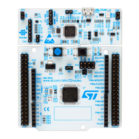
Figure 1. STM32 Nucleo-64 board top view
Picture is not contractual.
March 2021
UM2324 Rev 4
1/43
www.st.com
1
Advertisement
Table of Contents

Related Manuals for ST STM32G070RBT6


Summary of Contents for ST STM32G070RBT6
-
Page 1: Figure 1. Stm32 Nucleo-64 Board Top View
® ARDUINO Uno V3 connectivity and ST morpho headers provide easy means of expanding the functionality of the Nucleo open development platform with a wide choice of specialized shields. The STM32 Nucleo-64 boards do not require any separate probe, as they integrate the ST-LINK/V2-1 debugger/programmer. -
Page 2: Table Of Contents
Embedded ST-LINK/V2-1 ........14... - Page 3 Uno V3 connector ....... . . 29 CN7 and CN10 ST morpho connectors ......32 STM32 Nucleo-64 board information .
- Page 4 Contents UM2324 Revision history ........... . 42 4/43 UM2324 Rev 4...
- Page 5 ST-LINK jumper configuration ........
- Page 6 ST morpho connectors ........... . 32 Figure 17. STM32 Nucleo-64 boards ST morpho connector pinout ......33 6/43...
-
Page 7: Features
® – ARDUINO Uno V3 expansion connector – ST morpho extension pin headers for full access to all STM32 I/Os • Flexible power-supply options: ST-LINK, USB V , or external sources • On-board ST-LINK debugger/programmer with USB re-enumeration capability: mass storage, Virtual COM port, and debug port •... -
Page 8: Ordering Information
1. Additional information is available from the datasheet and reference manual of the target STM32. Table 1. Ordering information Order code Board reference Target STM32 NUCLEO-G070RB STM32G070RBT6 NUCLEO-G071RB MB1360 STM32G071RBT6 NUCLEO-G0B1RE STM32G0B1RET6 Codification The meaning of the codification is explained in Table Table 2. -
Page 9: Development Environment
STM32 Flash memory for easy demonstration of the device peripherals in standalone mode. The latest versions of the demonstration source code and associated documentation can be downloaded from www.st.com. Conventions Table 3 provides the conventions used for the ON and OFF settings in the present document. -
Page 10: Quick Start
[1-2], JP3 (IDD) on. For correct identification of all device interfaces from the host PC, install the Nucleo USB driver available on the www.st.com/stm32nucleo web page, before connecting the board. To power the board, connect the STM32 Nucleo-64 board to a PC with a USB Type-A ®... -
Page 11: Hardware Layout And Configuration
STM32 and its peripherals (STLINK/V2-1, pushbutton, LED, and morpho connectors). Figure 3 Figure 4 help the user to locate these features on the STM32 Nucleo-64 board. Figure 2. Hardware block diagram ST-LINK part Mini Embedded ST-LINK/V2-1 USER STM32... -
Page 12: Figure 3. Top Layout
Hardware layout and configuration UM2324 Figure 3. Top layout Figure 4. Bottom layout 12/43 UM2324 Rev 4... -
Page 13: Stm32 Nucleo-64 Board Mechanical Drawing
The STM32 Nucleo-64 board is divided into two parts: the ST-LINK part and the target MCU part. ST-LINK part PCB is cuttable to reduce board size. In this case, the rest target MCU part is only powered by VIN, E5V, and 3.3V on CN7 morpho connectors, or VIN and 3.3V on ®... -
Page 14: Embedded St-Link/V2-1
Standalone version doesn't exist (only Nucleo and future discovery support V2-1) For all general information concerning debugging and programming features common between V2 and V2-1 refer to ST-LINK/V2 user manual (UM1075). The embedded ST-LINK/V2-1 is usable in two different ways according to the jumper states (Refer to Table •... -
Page 15: Drivers
The ST-LINK/V2-1 embeds a firmware upgrade mechanism for the in-situ upgrade through the USB port. As the firmware may evolve during the lifetime of the ST-LINK/V2-1 product (for example new functionalities, bug fixes, support for new microcontroller families), it is recommended to keep the ST-LINK/V2-1 firmware up to date before starting to use an STM32 Nucleo-64 board. -
Page 16: Using St-Link/V2-1 To Program/Debug An External Stm32 Application
MSv48501V1 6.4.4 Using ST-LINK/V2-1 to program/debug an external STM32 application It is easy to use the ST-LINK/V2-1 to program the STM32 on an external application. Remove the 2 jumpers from CN4 as shown in Figure 8, and connect the application to the... -
Page 17: Power Supply And Power Selection
The STM32 Nucleo-64 board is designed to be powered by several DC power supplies. It is possible to supply the STM32 Nucleo-64 board with any of the following sources: • 5V_USB_STLK from the ST-LINK USB connector ® • VIN (7 V - 12 V) from ARDUINO connector or ST morpho connector •... -
Page 18: Table 7. Power Supply Capabilities
5V_ST_LINK is a DC power with limitations from the ST-LINK USB connector (USB type Micro-B connector of ST-LINK/V2-1). In this case, the JP2 jumper must be on pins 1 and 2 to select the STLK power source on the JP2 silkscreen. This is the default setting. If the USB enumeration succeeds, the STLK power is enabled, by asserting the PWR_ENn signal (from STM32F103CBT6). -
Page 19: Figure 9. Stlk Power Source
VIN is the 7 V to 12 V DC power from CN6 pin 8 named VIN on ARDUINO connector silkscreen or from pin 24 of CN7 ST morpho connector. In this case, the JP2 jumper must be on pins 3 and 4 to select the VIN power source on the JP2 silkscreen. In that case, the DC ®... -
Page 20: Figure 10. Jp2 [3-4]: Stlk Power Source
CN6 PIN8 MSv48504V1 E5V is the DC power coming from external (5V DC power from pin 6 of the CN7 ST morpho connector). In this case, the JP2 jumper must be on pins 5 and 6 to select the E5V power source on the JP2 silkscreen. -
Page 21: Figure 11. Jp2 [5-6]: Stlk Power Source
E5V: CN7 PIN6 MSv48505V1 5V_USB_CHARGER is the DC power charger connected to USB ST-LINK (CN2). To select the CHG power source on the JP2 silkscreen, the JP2 jumper must be on pins 7 and 8. In this case, if the STM32 Nucleo-64 board is powered by an external USB charger the debug is not available. -
Page 22: External Power Supply Output
Nucleo-64 board and the connected shield must be less than 500 mA. Programming/debugging when the power supply is not from ST-LINK VIN or E5V is usable as an external power supply in case the current consumption of the STM32 Nucleo-64 board and its extension boards exceed the allowed current on the USB. -
Page 23: Osc Clock Sources
Check that the green LED LD3 is turned ON, Connect the PC to the CN2 USB connector. If this sequence is not respected, the board may be powered by VBUS first from the ST- LINK, with the following risks: •... -
Page 24: Hse: Osc 8 Mhz Clock Supply
R33 and R34 OFF • MCO from ST-LINK: MCO output of ST-LINK is used as an input clock. This frequency cannot be changed, it is fixed at 8 MHz and connected to the PF0-OSC_IN of the STM32 microcontroller. The configuration must be: –... -
Page 25: Leds
Four LEDs are available on the STM32 Nucleo-64 board. The four LEDs are located on the top side of the board. LD1 COM: LD1 is a bi-colored LED. the LD1 default status is red. LD1 turns to green to indicate that communication is in progress between the PC and the ST-LINK/V2-1 as follow: –... -
Page 26: Idd Measurement
Table 9 describes the other available jumper settings. Table 9. Jumper configuration Jumper / Function State Comment ST-LINK/V2-1 enable for on-board ON [1-2] ON [3-4] MCU debugger T_SWCLK T_SWDIO ST-LINK/V2-1 functions enabled for OFF [1-2] OFF [3-4] external CN2 connector... - Page 27 UM2324 Hardware layout and configuration Table 10. Solder bridge configurations and settings (continued) Definition Bridge State Comment UART2 interface UART2 connect STLK and MCU on SB16/SB18 (reserved) board UART2 interface SB16/SB18 UART2 is used as GPIOs (reserved) Allowed current through CN2: 100 mA Allowed current through CN2 SB15...
-
Page 28: Connectors
CN7 and CN10: ST morpho connectors CN2 USB Micro-B connector The CN2 USB connector is used to connect the embedded ST-LINK/V2-1 to the PC for programming and debugging the STM32 Nucleo-64 board microcontroller. Figure 13. CN2 USB Micro-B connector (front view) -
Page 29: Arduino ® Uno V3 Connector
UM2324 Connectors ® ARDUINO Uno V3 connector ® The CN5, CN6, CN8, and CN9 ARDUINO connectors in Figure 14 are female connectors ® ® compatible with the ARDUINO standard. Most shields designed for ARDUINO fit the STM32 Nucleo-64 board. ® ®... -
Page 30: Table 12. Arduino ® Connector Pinout
Connectors UM2324 ® The related pinout for the ARDUINO connector is shown in Figure 15 Figure Note: listed in Table ® Figure 15. STM32 Nucleo-64 boards ARDUINO connector pinout ® Note: ARDUINO Uno V3 D0 and D1 signals are connected by default on USART1 (MCU I/O PC4 and PC5). - Page 31 UM2324 Connectors ® Table 12. ARDUINO connector pinout (continued) Connector Signal name STM32 pin Function number name SCL/D15 ARD_D15 I2C_1_SCL SDA/D14 ARD_D14 I2C_1_SDA AVDD VREF+ VREF+ SCK/D13 ARD_D13 SPI_1_SCK MISO/D12 ARD_D12 SPI_1_MISO PWM/MOSI/D11 ARD_D11 SPI_1_MOSI || TIM_14_CH1 PWM/CS/D10 ARD_D10 SPI_1_NSS || TIM_3_CH3 PWM/D9 ARD_D9 TIM_3_CH2...
-
Page 32: Cn7 And Cn10 St Morpho Connectors
Connectors UM2324 CN7 and CN10 ST morpho connectors The CN7 and CN10 ST morpho connectors are male pin headers accessible on both sides of the STM32 Nucleo-64 board (see Figure 16). All signals and power pins, except VDD_CORE 1.2 V of the STM32, are available on the ST morpho connectors. These connectors can also be probed by an oscilloscope, logical analyzer, or voltmeter. -
Page 33: Figure 17. Stm32 Nucleo-64 Boards St Morpho Connector Pinout
UM2324 Connectors The related pinout and the MCU assignment for the ST morpho connectors are listed in Figure 17 Figure Note:. Figure 17. STM32 Nucleo-64 boards ST morpho connector pinout ® Note: ARDUINO Uno V3 D0 and D1 signals are connected by default on USART1 (MCU I/O PA2 and PA3). -
Page 34: Stm32 Nucleo-64 Board Information
Any consequences deriving from such usage will not be at ST charge. In no event, ST will be liable for any customer usage of these engineering sample tools as reference designs or in production. -
Page 35: Nucleo-G071Rb Product History
UM2324 STM32 Nucleo-64 board information It embeds the STM32G070RBT6 microcontroller with silicon revision code "B". The limitations of this silicon revision are detailed in the errata sheet STM32G070CB/KB/RB device errata (ES0468). Product limitations No limitation identified for this product identification. -
Page 36: Board Revision History
Board MB1360 revision C-02 C23 and C24 are modified from 5.6 pF to 6.8 pF. T2 is modified from BSN20 to BSN20BK. This revision C-02 is produced with the STM32G070RBT6, STM32G071RBT6, or the latest STM32G0B1RET6 microcontroller. Board limitations No limitation identified for this board revision. -
Page 37: Appendix A Stm32 Nucleo-64 Board I/O Assignment
UM2324 STM32 Nucleo-64 board I/O assignment Appendix A STM32 Nucleo-64 board I/O assignment Table 13. STM32 Nucleo-64 board I/O assignment Pin No Pin name Signal or label Main feature / optional feature (SB) PC11 PC11 PC12 PC12 PC13 PC13 User Button/IO PC14 - OSC32_IN PC14 - OSC32_IN LSE CLK/IO... - Page 38 STM32 Nucleo-64 board I/O assignment UM2324 Table 13. STM32 Nucleo-64 board I/O assignment (continued) Pin No Pin name Signal or label Main feature / optional feature (SB) PB13 PB13 PB14 PB14 ARD_D6 || TIM_15_CH1 PB15 PB15 ARD_D7 ARD_D8 ARD_D9 || TIM_3_CH2 PA10 PA10 ARD_D2...
-
Page 39: Appendix B Federal Communications Commission (Fcc) And Ised Canada Compliance Statements
UM2324 Federal Communications Commission (FCC) and ISED Canada Compliance Statements Appendix B Federal Communications Commission (FCC) ISED Canada Compliance Statements FCC Compliance Statement Part 15.19 This device complies with Part 15 of the FCC Rules. Operation is subject to the following two conditions: (1) this device may not cause harmful interference, and (2) this device must accept any interference received, including interference that may cause undesired operation. -
Page 40: Ised Compliance Statement
Federal Communications Commission (FCC) and ISED Canada Compliance Statements UM2324 ISED Compliance Statement This device complies with FCC and ISED Canada RF radiation exposure limits set forth for general population for mobile application (uncontrolled exposure). This device must not be collocated or operating in conjunction with any other antenna or transmitter. -
Page 41: Appendix Cce Conformity
UM2324 CE conformity Appendix C CE conformity Warning EN 55032 / CISPR32 (2012) Class B product Warning: this device is compliant with Class B of EN 55032 / CISPR32. In a residential environment, this equipment may cause radio interference. Avertissement : cet équipement est conforme à la Classe B de la EN 55032 / CISPR 32. Dans un environnement résidentiel, cet équipement peut créer des interférences radio. -
Page 42: Table 14. Document Revision History
Revision history UM2324 Revision history Table 14. Document revision history Date Revision Changes 24-Oct-2018 Initial version 26-Oct-2018 Added NUCLEO-G070RB board Added NUCLEO-G0B1RE board Entire document reorganized – Updated: Introduction, Features, Ordering information, Development environment, Development toolchains, 19-Nov-2020 Demonstration software. – Added: Codification, Section 8: STM32 Nucleo-64 board information,... - Page 43 ST products and/or to this document at any time without notice. Purchasers should obtain the latest relevant information on ST products before placing orders. ST products are sold pursuant to ST’s terms and conditions of sale in place at the time of order acknowledgement.
- Page 44 Mouser Electronics Authorized Distributor Click to View Pricing, Inventory, Delivery & Lifecycle Information: STMicroelectronics NUCLEO-G0B1RE...
Need help?
Do you have a question about the STM32G070RBT6 and is the answer not in the manual?
Questions and answers