Table of Contents
Advertisement
Quick Links
UM1878
User manual
Evaluation board with STM32L073VZ MCU
Introduction
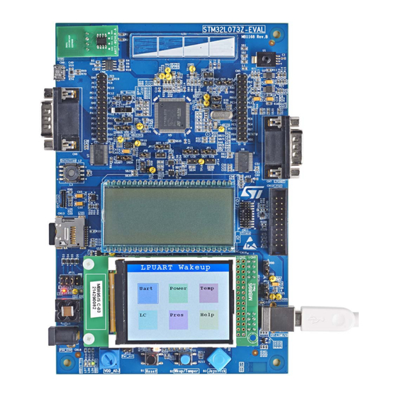
The STM32L073Z-EVAL Evaluation board is designed as a complete demonstration and
®
®
development platform for the STMicroelectronics Arm
Cortex
-M0+ core-based
2
STM32L073VZT6 microcontroller with three I
Cs, two SPIs, four USARTs, one UART, one
12-bit ADC, two 12-bit DACs, LCD driver, up to 192-Kbyte flash memory, 20-Kbyte RAM,
6-Kbyte EEPROM, touch sensing, USB FS, LCD controller, SWD debugging support. This
Evaluation board can be used as a reference design for user application development but is
not considered as a final application.
The full range of hardware features on the board helps the user to evaluate all peripherals
(USB FS, RS-232, USART, 12-bit ADC and DAC, color TFT LCD, LCD segments, low-
power UART, IrDA, microSD™ card, touch-sensing slider, pressure measurement,
temperature measurement, LC sensor metering) and to develop applications. The extension
headers offer the possibility to connect a daughterboard or a wrapping board for a specific
application.
An embedded ST-LINK/V2-1 debugger facilitates the software development and the
programming of the STM32L073VZT6 microcontroller.
Figure 1. STM32L073Z-EVAL Evaluation board
Picture is not contractual.
January 2024
UM1878 Rev 3
1/57
www.st.com
1
Advertisement
Table of Contents

Related Manuals for ST STM32L073Z-EVAL E


Summary of Contents for ST STM32L073Z-EVAL E
- Page 1 LC sensor metering) and to develop applications. The extension headers offer the possibility to connect a daughterboard or a wrapping board for a specific application. An embedded ST-LINK/V2-1 debugger facilitates the software development and the programming of the STM32L073VZT6 microcontroller. Figure 1. STM32L073Z-EVAL Evaluation board Picture is not contractual.
-
Page 2: Table Of Contents
Embedded ST-LINK/V2-1 ........11... - Page 3 UM1878 Contents 4.11 Virtual COM port ..........21 4.11.1 Limitations .
- Page 4 ST-LINK/V2-1 programming connector CN15 ..... 46 ST-LINK/V2-1 USB Type-B connector CN17 ..... . 46 SWD connector CN12 .
- Page 5 UM1878 List of tables List of tables Table 1. List of available products ........... 8 Table 2.
- Page 6 List of figures UM1878 List of figures Figure 1. STM32L073Z-EVAL Evaluation board ......... 1 Figure 2.
-
Page 7: Features
RF-EEPROM daughterboard expansion – Extension for daughterboard or wrapping board • Four 5 V power supply options: power jack, ST-LINK USB connector, user USB FS connector, or daughterboard • On-board ST-LINK/V2-1 debugger/programmer with USB re-enumeration capability: mass storage, Virtual COM port, and debug port •... -
Page 8: Ordering Information
Ordering information UM1878 Ordering information To order the STM32L073Z-EVAL Evaluation board, refer to Table 1. Additional information is available from the datasheet and reference manual of the target STM32. Table 1. List of available products Order code Board reference Target STM32 –... -
Page 9: Development Environment
STM32 flash memory for easy demonstration of the device peripherals in standalone mode. The latest versions of the demonstration source code and associated documentation can be downloaded from www.st.com. a. Windows is a trademark of the Microsoft group of companies. ®... -
Page 10: Hardware Layout And Configuration
RS-232 RS-232 LCD segment LPUART transceiver connector 40×8 Differential Pressure Virtual COM ADC 16 bits amplifier sensor port USART4 Embedded ST-LINK/V2-1 Temperature USB Type-B sensor connector STM32L073VZ RF-EEPROM connector connectors Extension connector DAC output Joystick expander ADC input LP timer... -
Page 11: Embedded St-Link/V2-1
4-color LEDs (RV1) (B2) (LD1, LD2, LD3, LD4) Reset button Joystick (B1) (B3) MSv37069V2 Embedded ST-LINK/V2-1 The ST-LINK/V2-1 programming and debugging tool is integrated on the STM32L073Z-EVAL Evaluation board. Compared to ST-LINK/V2 the changes are listed below. UM1878 Rev 3 11/57... -
Page 12: Drivers
• SWIM interface For all general information concerning debugging and programming features common between V2 and V2-1 please refer to ST-LINK/V2 user manual (UM1075) and technical note (TN1235). Known limitation: Activating the readout protection on ST-LINK/V2-1 target, prevents the target application from running afterwards. -
Page 13: St-Link/V2-1 Firmware Upgrade
ST-LINK/V2-1 facility for debug and programming of the target microcontroller STM32L073VZT6 is integrated on the STM32L073Z-EVAL Evaluation board. For its own operation, ST-LINK/V2-1 employs a dedicated MCU with flash memory. Its firmware determines ST-LINK/V2-1 functionality and performance. The firmware may evolve during the life span of STM32L073Z-EVAL to include new functionality, fix bugs, or support new target microcontroller families. -
Page 14: Table 3. Power Related Jumpers
U5V location, as following: JP11 MSv37083V1 To supply STM32L073Z-EVAL only from the USB connector CN17 of ST-LINK/V2, set the jumper JP11 to STlk location, as showed in the below figure. In this case, the jumper of ST-LINK JP13 must be opened. - Page 15 UM1878 Hardware layout and configuration Table 3. Power related jumpers (continued) Jumper Description To supply both STM32L073Z-EVAL and a daughterboard connected to extension connectors CN4 and CN5, (daughterboard must have its own power supply not connected), set jumpers to E5V and D5V locations, as following: JP11 MSv37085V1 (pins V...
-
Page 16: Adjustable Power Supply
JP5 and connect an ampere-meter to JP5, positive terminal to pin 1, negative to pin MSv37091V1 By default JP13 is not connected to let ST-LINK detect automatically if it should provide the supply of the board from ST-LINK USB V (default setting). -
Page 17: Clock Source
UM1878 Hardware layout and configuration to adjust the voltage from 1.65 V to 3.6 V. The three LEDs LD7, LD8, LD9 warn the user that voltage is below 1.7 V or above 1.8 V. Clock source Two clock sources are available for the microcontroller STM32L073VZT6 on the Evaluation board STM32L073Z-EVAL: •... -
Page 18: Boot Option
From a daughterboard connected to extension connectors, RESET is pin 24 of connector CN5. • Embedded ST-LINK/V2-1 • RS-232 connector CN6 for ISP. Jumper JP6 must be closed for RESET to be handled by pin 8 of RS-232 connector CN6 (CTS signal). -
Page 19: Usb Fs
UM1878 Hardware layout and configuration Table 7. Boot related jumper Jumper Description By default, BOOT0 is only controlled by switch SW1. jumper not fitted (default setting) BOOT0 can be forced high with terminal 6 of CN6 connector (RS-232 DSR line). This configuration is used to allow the device connected via RS-232 to initiate STM32L073VZT6 programming process. -
Page 20: Limitations
Hardware layout and configuration UM1878 Table 8. Temperature sensor related solder bridge Solder bridge Description Closed Temperature sensor address set to 0x92. (default setting) Open Temperature sensor address set to 0x90. To enable SMBus functionality, the LCD segment daughterboard must be mounted on the “IO”... -
Page 21: Limitations
4.11 Virtual COM port RX and TX of USART4 are available in a USB Virtual COM port managed by the ST- LINK/V2-1. The USB connector of ST-LINK/V2-1 is CN17. Virtual COM port can be used over the whole operating voltage range of the microcontroller because level shifters are used. -
Page 22: Limitations
Hardware layout and configuration UM1878 By default, the serial communication settings are: 115200 bit/s, 8 bits, no parity, 1 stop bit, no flow control. 4.11.1 Limitations No limitation. 4.11.2 Operating voltage The Virtual COM port is operating over the whole V range: 1.65 V to 3.6 V. -
Page 23: Figure 6. Location Of Adc Input Connector Cn2
UM1878 Hardware layout and configuration Figure 6. Location of ADC input connector CN2 ADC_IN5 MSv37095V1 A low-pass filter can be implemented for the ADC input by replacing R7 and C2 by appropriate values depending on the application. Figure 7. Provision for filter implementation As the port PA5 can be used also a DAC output, the STM32L073Z-EVAL Evaluation board gives also provision to build an output filter structure by replacing R8 and C2 by appropriate values. -
Page 24: Operating Voltage
Hardware layout and configuration UM1878 4.13.1 Operating voltage ADC input is operational with V > 1.8 V. 4.14 Analog output DAC The analog output DAC_OUT1 (port PA4) of microcontroller STM32L073VZT6 is available at connector CN3 located below the touch-sensing slider as shown below. The left pin of CN3 is the connection of GND reference, and right pin is DAC output voltage. -
Page 25: Limitations
UM1878 Hardware layout and configuration Table 11. Analog input related jumper JP2 settings Jumpers and resistors Description 2 and 3 connected LC sensor metering use: PA4 is connected to the capacitor C59 to filter the DAC_OUT1 voltage for LC sensor metering. DAC_OUT1 is connected internally to the inverting input of the internal comparator Comp2 (refer to Section 4.20.1: LC sensor metering principle... -
Page 26: Tft Lcd Display
Hardware layout and configuration UM1878 4.15 TFT LCD display The 2.4” color TFT LCD is connected to SPI1 port of STM32L073VZT6. The TFT LCD daughterboard is the MB895-Serial. Table 12. TFT LCD connector 2.4” TFT LCD connector CN16 Description Pin connection Description Pin connection PE10... -
Page 27: Input Devices
UM1878 Hardware layout and configuration 4.17 Input devices The 4-direction joystick B3 with selection, Wake-up/ Tamper button B2, Reset button B1 are available as input devices. Table 14. Input devices Input devices Pin used Circuit Joystick SEL GPIO0 MFX U25 Joystick DOWN GPIO1 MFX U25... -
Page 28: Table 15. Lcd Segments 21 To 28 Mapping Table
Hardware layout and configuration UM1878 Figure 10. LCD segment daughterboard in LCD position Figure 11. LCD segment daughterboard in “IO” position The signal mapping of each LCD segment is detailed in the following table (rows are LCD_COMx, columns LCD_SEGy, with x comprised between 0 and 7, y from 0 to 39): Table 15. -
Page 29: Table 16. Lcd Segments 0 And 29 To 39 Mapping Table
UM1878 Hardware layout and configuration Table 16. LCD segments 0 and 29 to 39 mapping table COM7 9g 13g 14g 15g 16g 17g COM6 9h 13h 14h 15h 16h 17h COM5 9i COM4 9j COM3 9d 13d 14d 15d 16d 17d COM2 9c COM0 9e 13e 14e 15e 16e 17e... -
Page 30: Table 19. Lcd Segments Related Jumpers And Solder Bridges
Hardware layout and configuration UM1878 Figure 12. LCD segment names Table 19. LCD segments related jumpers and solder bridges Jumpers, solder Description bridges, resistors JP8 closed The LC network (L2 or L3, and C40) on STM32L073Z-EVAL is used for LC sensor MSv37092V1 metering. -
Page 31: Limitations
UM1878 Hardware layout and configuration Table 19. LCD segments related jumpers and solder bridges (continued) Jumpers, solder Description bridges, resistors JP1, JP15, JP17, JP2: 2,3 closed LC sensor metering is used, exclusive with LCD segments and DAC output. JP1, JP15, JP17 with pins 2 and 3 closed: ports PA7, PB4, PC0 are used for LC sensor metering signals: DET_COMP2_OUT, DET_COMP2_INP, DET_LPTIM_CH1 JP14, JP16, respectively. -
Page 32: Lc Sensor Metering Principle
Hardware layout and configuration UM1878 4.20.1 LC sensor metering principle Figure 13. Functional block diagram of LC sensor metering Microcontroller STM32L073VZ Damped oscillations centered on V GPIO Output LPTIM Comp2 from DAC_OUT1 LC sensor Power control GPIO Output Follower amplifier AC voltage = GROUND DC voltage = V MSv40707V2... -
Page 33: Lc Sensor Metering Description
UM1878 Hardware layout and configuration available at port PB4 with a superimposition of a DC voltage of V /2 respectively to the ground. After the comparator threshold controlled by the DAC_OUT1 voltage is set properly by a calibration, the comparator delivers pulses to the low-power timer LPTIM. LPTIM is in charge to count the number of oscillations. -
Page 34: Table 20. Solder Bridges And Jumpers For Lc Sensor Metering
Hardware layout and configuration UM1878 The threshold of the comparator is the voltage on the negative input of Comp2. It is generated by the DAC_OUT1 connected internally inside the microcontroller. The DAC_OUT1 voltage must be set to a voltage a bit higher to V /2, typically a few 10 mV over V /2. -
Page 35: Limitations
UM1878 Hardware layout and configuration Table 20. Solder bridges and jumpers for LC sensor metering (continued) Jumpers, solder bridges, Description resistors JP1, JP15, JP17, JP2: 2,3 closed LC sensor metering is used, and is exclusive with LCD segments and DAC output. JP1, JP15, JP17 with pins 2 and 3 closed: ports PA7, PB4, PC0 are used for LC sensor metering signals: DET_COMP2_OUT, DET_COMP2_INP, JP14, JP16, JP18:... -
Page 36: Table 21. Sensor Differential Voltage
Hardware layout and configuration UM1878 Table 21. Sensor differential voltage Pressure Sensor differential voltage 0 hPa 0 mV 800 hPa 10.56 mV 1000 hPa 13.2mV 1200 hPa 15.84 mV As the proposed pressure measurement targets only barometric use, the sensor is used only in the range from 800 hPa to 1000 hPa, then the amplification is centered on this range. -
Page 37: Errors
UM1878 Hardware layout and configuration Table 22. Differential voltage Sensor differential voltage Pressure Differential V 0 hPa 0 mV Saturated at - 800 hPa 10.56 mV -1.3 V 1000 hPa 13.2 mV 1200 hPa 15.84 mV +1.23 V Finally, in STM32L073Z-EVAL Evaluation board, the differential voltage is shifted by a V offset and changed in a single voltage by the last unity gain operational amplifier. -
Page 38: Limitations
Hardware layout and configuration UM1878 A first-order low pass with 3 Hz cut-off frequency, is composed of 47 kΩ resistors combined with 1 μF capacitors to feedback the first amplifiers U3A and U3B. 4.21.5 Limitations No exclusivity. 4.21.6 Operating voltage Operating voltage is fixed at: +3.3 V 4.22 Touch-sensing slider... -
Page 39: Limitations
UM1878 Hardware layout and configuration Table 24. Touch sensing related solder bridges (continued) Settings Solder STM32 enable Description bridges port touch sensing SB10 Close Connects the charge capacitor to PA2. Open Disconnects PA2 from track to LCD segments to avoid disturbances. Figure 16. -
Page 40: Idd Auto-Measurement
Hardware layout and configuration UM1878 Table 25. Extension connectors pin-out CN4 (left side) CN5 (right side) Signal Signal +3V3 PE10 PE11 PE12 PE13 PH10 PE14 PC14 PC15 PE15 PC13 PA11 PA13 PA12 VLCD PA14 BOOT0 RESET# 4.24 IDD auto-measurement In addition to the jumpers allowing the measurement of each power domain separately or the whole microcontroller consumption, the STM32L073Z-EVAL Evaluation board offers also an automatic consumption measurement. -
Page 41: Analog Section Description
UM1878 Hardware layout and configuration Table 26. IDD auto-measurement related jumper settings Jumper Description JP10 2 and 3 closed (jumper in IDD position): STM32L073VZT6 is powered through IDD measurement circuit. JP10 1 and 2 closed (jumper in position): JP10 IDD measurement circuit is bypassed, STM32L073VZT6 is powered directly. (default setting) JP10: no jumper to pins 1, 2, 3. -
Page 42: Difference Amplifier
Hardware layout and configuration UM1878 The voltage drop across the selected shunt is amplified by a very high accuracy and zero-drift operational amplifier. The voltage drop is connected to pins 3 and 5 of the operational amplifier U21. The digital section switches or not to a higher resistance shunt for a better measurement, depending on the measurement result obtained with one shunt. -
Page 43: Figure 19. Digital Section Schematic
UM1878 Hardware layout and configuration Figure 19. Digital section schematic Multi Function eXpander one capacitor close to each MFX pins: VDD, VDD_1, VDD_2, VDD_3 R166 BEAD MFX_IRQOUT C106 C116 PE6 can also be used to wake-up the MCU 100nF 100nF 100nF 100nF 100nF... -
Page 44: Connectors
Connectors UM1878 Connectors RS-232 connector CN6 Figure 20. RS-232 connector CN6 (front view) MS30720V1 Table 27. RS-232 connector CN6 Pin number Description Description number Bootloader_BOOT0 RX (PD6) RTS (PD4) TX (PD5) CTS/ Bootloader_RESET Power connector CN18 STM32L073Z-EVAL Evaluation board can be powered from a DC 5 V power supply via the external power supply jack (CN18) shown in Figure 21: Power supply connector CN18. -
Page 45: Lcd Segment Daughterboard Connectors Cn10 And Cn14
UM1878 Connectors LCD segment daughterboard connectors CN10 and CN14 Two 48-pins male headers CN10 and CN14 are used to connect with the LCD segment daughterboard (MB979). The space between these two connectors and the position of every LCD segment signals are defined as a standard, which allows the development of common daughterboards for several Evaluation boards. -
Page 46: St-Link/V2-1 Programming Connector Cn15
It is not populated by default and not for end user. ST-LINK/V2-1 USB Type-B connector CN17 The USB connector CN17 is used to connect the embedded ST-LINK/V2-1 to the PC for board debugging. Figure 22. USB Type-B connector CN17 Table 29. -
Page 47: Swd Connector Cn12
UM1878 Connectors SWD connector CN12 Figure 23. Trace debugging connector CN12 (top view) MS30722V2 Table 30. SWD debugging connector CN12 Pin number Description Pin number Description power power SWDIO PA13 SWCLK PA14 RESET# DBGRQ DBGACK Trace debugging connector CN11 Figure 24. Trace debugging connector CN11 (top view) MS30722V2 UM1878 Rev 3 47/57... -
Page 48: Microsd™ Connector Cn13
Connectors UM1878 Table 31. Trace debugging connector CN11 Pin number Description Description number power SWDIO PA13 SWCLK PA14 Pin is removed RESET# microSD™ connector CN13 Figure 25. microSD™ connector CN13 Table 32. microSD™ connector CN13 Description Description number number MicroSD_CS (PD0) SPI_MISO (PE14) SPI_MOSI (PE15) +3V3... -
Page 49: Rf-Eeprom Daughterboard Connector Cn1
UM1878 Connectors RF-EEPROM daughterboard connector CN1 Figure 26. RF-EEPROM daughterboard connector CN1 (front view) MS30715V2 Table 33. RF-EEPROM daughterboard connector CN1 Pin number Description Pin number Description I2C_SDA (PG13) I2C_SCL (PG14) EXT_RESET(PC6) UM1878 Rev 3 49/57... -
Page 50: Mechanical Dimensions
Mechanical dimensions UM1878 Mechanical dimensions Figure 27. Mechanical dimensions 114.3mm 68.59mm 21.52mm 3.5 mm 5.715mm 5.715mm MSv40709V1 50/57 UM1878 Rev 3... -
Page 51: Stm32L073Z-Eval Evaluation Board Information
Parts marked as "ES" or "E" are not yet qualified and therefore not approved for use in production. ST is not responsible for any consequences resulting from such use. In no event will ST be liable for the customer using any of these engineering samples in production. -
Page 52: Stm32L073Z-Eval Product History
STM32L073Z-EVAL Evaluation board information UM1878 STM32L073Z-EVAL product history Table 34. Product history Order Product Product change Product details Product limitations code identification description MCU: – STM32L073VZT6 revision “Z” MCU errata sheet: – STM32L07xxx/L08xxx device errata (ES0292) Boards: – MB895-Serial-C03 (TFT LCD daughterboard) STM32L073Z- Initial revision... -
Page 53: Board Revision History
UM1878 STM32L073Z-EVAL Evaluation board information Board revision history Table 35. Board revision history Board variant and Board change Board reference Board limitations revision description Default-C03 Initial revision No limitation Several part references updated due to MB895 obsolescence (such as (TFT LCD daughterboard) Serial-C04 No limitation inductor or others, refer... -
Page 54: Federal Communications Commission (Fcc) And Ised Canada Compliance Statements
Federal Communications Commission (FCC) and ISED Canada Compliance Statements UM1878 Federal Communications Commission (FCC) and ISED Canada Compliance Statements FCC Compliance Statement 8.1.1 Part 15.19 This device complies with Part 15 of the FCC Rules. Operation is subject to the following two conditions: (1) this device may not cause harmful interference, and (2) this device must accept any interference received, including interference that may cause undesired operation. -
Page 55: Ised Compliance Statement
UM1878 Federal Communications Commission (FCC) and ISED Canada Compliance Statements ISED Compliance Statement Compliance Statement ISED Canada ICES-003 Compliance Label: CAN ICES-3 (B) / NMB-3 (B). Déclaration de conformité Étiquette de conformité à la NMB-003 d'ISDE Canada : CAN ICES-3 (B) / NMB-3 (B). UM1878 Rev 3 55/57... -
Page 56: Revision History
Chapter 8: Federal Communications Commission (FCC) and ISED Canada Compliance Statements. Updated JP7 description in Table 3: Power related jumpers. Updated Section 4.1: Embedded ST-LINK/V2-1. Updated Figure 2: Hardware block diagram, Figure 3: 30-Jan-2024 STM32L073Z-EVAL Evaluation board (top view), and... - Page 57 ST products and/or to this document at any time without notice. Purchasers should obtain the latest relevant information on ST products before placing orders. ST products are sold pursuant to ST’s terms and conditions of sale in place at the time of order acknowledgment.
Need help?
Do you have a question about the STM32L073Z-EVAL E and is the answer not in the manual?
Questions and answers