
Subscribe to Our Youtube Channel
Related Manuals for Analog Devices ADZS-BF707-BLIP2


Summary of Contents for Analog Devices ADZS-BF707-BLIP2
- Page 1 ADZS-BF707-BLIP2 Board Evaluation System Manual Revision 1.0, April 2015 Part Number 82-100126-01 Analog Devices, Inc. One Technology Way Norwood, Mass. 02062-9106...
- Page 2 Analog Devices, Inc. Printed in the USA. Disclaimer Analog Devices, Inc. reserves the right to change this product without prior notice. Information furnished by Analog Devices is believed to be accurate and reliable. However, no responsibility is assumed by Analog Devices for its use;...
- Page 3 Regulatory Compliance The ADZS-BF707-BLIP2 board is designed to be used solely in a labora- tory environment. The board is not intended for use as a consumer end product or as a portion of a consumer end product. The board is an open system design which does not include a shielded enclosure and therefore may cause interference to other electrical devices in close proximity.
-
Page 5: Table Of Contents
What’s New in This Manual ............xiii Technical Support ................xiv Supported Processors ..............xiv Supported Tools ................xv Product Information ............... xv Analog Devices Web Site ............xv EngineerZone ................xvi Notation Conventions ..............xvi ADZS-BF707-BLIP2 Board Evaluation System Manual... - Page 6 UART1 Interface ................1-8 USB Interface ................1-8 SD Interface ................. 1-9 Debug Interface ................1-9 Power-On-Self Test ............... 1-9 RF Wireless Interface ..............1-9 Power Architecture ..............1-10 Example Programs ..............1-10 Reference Design Information ............. 1-11 ADZS-BF707-BLIP2 Board Evaluation System Manual...
- Page 7 USB Connector (P4) ............. 2-10 USB to UART Connector (P8) ..........2-10 Power Connector (P5) ............2-11 RF Wireless Connector (J2) ........... 2-11 SD Connector (J3) ..............2-11 ADZS-BF707-BLIP2 BOARD BILL OF MATERIALS ADZS-BF707-BLIP2 BOARD SCHEMATIC INDEX ADZS-BF707-BLIP2 Board Evaluation System Manual...
- Page 8 Contents viii ADZS-BF707-BLIP2 Board Evaluation System Manual...
- Page 9 Blackfin products. The ADZS-BF707-BLIP2 board is shipped with all of the necessary hard- ware—you can start the evaluation immediately. The package contains the standalone evaluation board, CE-approved power supply, and USB cable.
-
Page 10: Product Overview
• 24 MHz crystal oscillator for USB • Mobile DDR memory (DMC0) chip • 32M bit x 16 x 4 banks (2G bit) • MT46H128M16LFDD-48WT • Quad SPI Flash (SPI2) • 32M bit serial flash memory • Windbond W25Q32 ADZS-BF707-BLIP2 Board Evaluation System Manual... - Page 11 • FTDI FT232RQ USB to UART converter • USB Mini B connector • USB interface • Micro AB connector • RESET controller • Analog Devices ADM6315 microprocessor supervisory circuits • Debug (JTAG/SWD/SWO) interface • JTAG/SWD/SWO 10-pin 0.05” header for use with Analog Devices emulators •...
-
Page 12: Purpose Of This Manual
(board). The text describes operation and configuration of the board components and pro- vides guidelines for running your own code on the ADZS-BF707-BLIP2 board. Finally, a schematic and a bill of materials are provided for reference. -
Page 13: Manual Contents
Provides a list of hardware components used to manufacture the BLIP2 board. • Appendix B, ADZS-BF707-BLIP2 Board Schematic Lists the resources for board-level debugging. What’s New in This Manual This is the first edition (Revision 1.0) of the ADZS-BF707-BLIP2 Board Evaluation System Manual. ADZS-BF707-BLIP2 Board Evaluation System Manual xiii... -
Page 14: Technical Support
Technical Support Technical Support You can reach Analog Devices processors and DSP technical support in the following ways: • Post your questions in the processors and DSP support community ® at EngineerZone http://ez.analog.com/community/dsp • Submit your questions to technical support directly at: http://www.analog.com/support... -
Page 15: Supported Tools
Information on supported tools for the ADZS-BF707-BLIP2 board and the ADSP-BF70x family of processors is: http://www.analog.com/BLIP Product Information Product information can be obtained from the Analog Devices Web site and the online help system. Analog Devices Web Site The Analog Devices Web site, , provides information www.analog.com... -
Page 16: Engineerzone
If you are a registered user, just log on. Your user name is your e-mail address. EngineerZone EngineerZone is a technical support forum from Analog Devices. It allows you direct access to ADI technical support engineers. You can search FAQs and technical information to get quick answers to your embedded processing and DSP design questions. - Page 17 A Warning identifies conditions or inappropriate usage of the product that could lead to conditions that are potentially hazardous for the devices users. In the online version of this book, the word Warning appears instead of this symbol. ADZS-BF707-BLIP2 Board Evaluation System Manual xvii...
- Page 18 Notation Conventions xviii ADZS-BF707-BLIP2 Board Evaluation System Manual...
-
Page 19: Using Adzs-Bf707-Blip2 Board
1 USING ADZS-BF707-BLIP2 BOARD This chapter provides information to assist you with development of pro- grams for the ADZS-BF707-BLIP2 evaluation system. The following topics are covered. • Package Contents • Default Configuration • BLIP2 Board Installation • BLIP2 Board Session Startup •... -
Page 20: Package Contents
Analog Devices, Inc. if any item is missing. Default Configuration The ADZS-BF707-BLIP2 board is designed to run as a standalone unit. When removing the BLIP2 board from the package, handle the board carefully to avoid the discharge of static electricity, which can damage some components. -
Page 21: Blip2 Board Installation
Please refer to the appropriate emulator manual if the sta- tus LED does not turn on. 3. Attach the emulator header ( ) on the bottom of the ICE-1000 to connector on the BLIP2 board. ADZS-BF707-BLIP2 Board Evaluation System Manual... -
Page 22: Blip2 Board Session Startup
Note that CCES is not connected to the target board. 2. Use the Debug Configurations wizard to connect to the BLIP2 board. If a debug configuration exists already, select the appropriate configuration and click Debug. Go to step 8. ADZS-BF707-BLIP2 Board Evaluation System Manual... - Page 23 9. Select the Custom Board Support tab and check the Enable cus- tomizations box. Click on Browse and select the ADZS-BF707-BLIP2-proc.xml file found in the ADZS_BF707_BLIP2_Board-Rel1.0.0\Blackfin\Examples folder. ADZS-BF707-BLIP2 Board Evaluation System Manual...
-
Page 24: Evaluation License
When prompted, choose “I have a serial num- ber that I would like to activate” and enter the serial number shown on the card. If the evaluation license is installed but not activated, it allows ADZS-BF707-BLIP2 Board Evaluation System Manual... -
Page 25: Mobile Ddr Memory
• Analog Devices directly. Call (800) 262-5645 or 781-937-2384 or go to: http://www.analog.com/buyonline • Analog Devices, Inc. local sales office or authorized distributor. To locate one, go to: www.analog.com/adi-sales Mobile DDR Memory The ADSP-BF707 processor connects to a 2Gb Micron MT46H128M16 chip through the Double Data Rate Synchronous Dynamic Ran- dom-Access Memory controller. -
Page 26: Spi Flash
AB connector. The board supports USB high speed mode. To learn about the device and host modes of the processor, refer to the USB example, which is included in the ADZS-BF707-BLIP2 Board Sup- port Package. For more information, refer to the ADSP-BF70x Blackfin+ Processor Hardware Reference. -
Page 27: Sd Interface
POST. RF Wireless Interface A RF Wireless connector allows the BLIP2 board to be connected to an Analog Devices Inc. Wireless Sensor Network (WSN) cluster board EV-ADRN-WSN-2Z. Alternatively, it can be used as a general-purpose ADZS-BF707-BLIP2 Board Evaluation System Manual... -
Page 28: Power Architecture
ADZS-BF707-BLIP2 Board Schematic. Power Architecture The ADZS-BF707-BLIP2 board has three primary voltage domains: 3.2V, 1.1V, and 1.8V. The power input is a 5V wall adaptor. The Analog Devices ADP2370 voltage regulator provides 3.2V for the signal and the 3.2V power requirements of the board. The VDD_EXT ADP2230 voltage regulator provides 1.1V for the... -
Page 29: Reference Design Information
A reference design info package is available for download on the Analog Devices Web site. The package provides information on the design, lay- out, fabrication, and assembly of the BLIP2 board. The information can be found at: http://www.analog.com/BLIP ADZS-BF707-BLIP2 Board Evaluation System Manual 1-11... - Page 30 Reference Design Information 1-12 ADZS-BF707-BLIP2 Board Evaluation System Manual...
-
Page 31: Adzs-Bf707-Blip2 Board Hardware Reference
2 ADZS-BF707-BLIP2 BOARD HARDWARE REFERENCE This chapter describes the hardware design of the ADZS-BF707-BLIP2 board. The following topics are covered. • System Architecture Describes the board’s configuration and explains how the board components interface with the processor. • Push Buttons Shows the locations and describes the push buttons. -
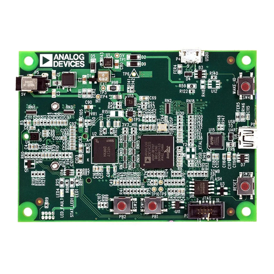
Page 32: System Architecture
USB Mini connector Figure 2-1. BLIP2 Board Block Diagram The ADZS-BF707-BLIP2 board is designed to demonstrate the image analysis capabilities of the ADSP-BF707 processor. The board houses two imaging sensors. ASX340AT is a CMOS imaging sensor made by Aptina/ON Semiconductor. It is placed underneath a M12 lens holder. - Page 33 OVM7692 is a camera module made by Omnivision. It packages an OV7692 imaging sensor with a lens. The ADZS-BF707-BLIP2 board has a 24 MHz input clock and runs at 384 MHz internally. USB circuitry and a micro USB AB connector enable the BLIP2 board to connect to a host.
-
Page 34: Push Buttons
Push Buttons Push Buttons This section describes operation of the push buttons. The push button locations are shown in Figure 2-2. Figure 2-2. Push Button Locations ADZS-BF707-BLIP2 Board Evaluation System Manual... -
Page 35: Gpio Push Buttons (Sw1 And Sw2)
) resets the following ICs: processor ( )and the USB to UART converter ( WAKE IO Push Button (SW4) The WAKE IO push button ( ) wakes up the processor after it goes into hibernate mode. ADZS-BF707-BLIP2 Board Evaluation System Manual... -
Page 36: Leds
LEDs LEDs This section describes the on-board LEDs. Figure 2-3 shows the LED locations. Figure 2-3. LED Locations ADZS-BF707-BLIP2 Board Evaluation System Manual... -
Page 37: Gpio Status Led (Led1)
, it indicates the status of LED1 the board. SYS_FAULT LED (LED4) When the SYS_FAULT LED ( ) (red) is , it indicates a system fault. LED4 For more information, refer to the ADSP-BF70x Blackfin+ Processor Hard- ware Reference. ADZS-BF707-BLIP2 Board Evaluation System Manual... -
Page 38: Connectors
Connectors Connectors This section describes connector functionality and provides information about mating connectors. The connector locations are shown in Figure 2-4 Figure 2-5. Figure 2-4. Connector Locations, Top ADZS-BF707-BLIP2 Board Evaluation System Manual... - Page 39 ADZS-BF707-BLIP2 Board Hardware Reference Figure 2-5. Connector Locations, Bottom ADZS-BF707-BLIP2 Board Evaluation System Manual...
-
Page 40: Jtag/Swd/Swo Connector (P3)
The JTAG/SWD/SWO header ( ) provides debug connectivity for the processor. This is a 0.05” shrouded through-hole connector from SAM- TEC (SAMTEC_SHF-105-01-L-D-SM-K). This connector mates with ICE-1000, ICE-2000, and any newer Analog Devices emulators. For more information, see Debug Interface. -
Page 41: Power Connector (P5)
4 x 2 0.05” pitch socket SAMTEC SFMC-104-T1-L-D Mating Connector 4 x 2 0.05” pitch header SAMTEC FTSH-104-04-F-D SD Connector (J3) Part Description Manufacturer Part Number SD 8-bit, 2 GB SANDISK MHC-W21-601 Mating Connector 2 GB SANDISK SDSDB-2048-A11 ADZS-BF707-BLIP2 Board Evaluation System Manual 2-11... - Page 42 Connectors 2-12 ADZS-BF707-BLIP2 Board Evaluation System Manual...
- Page 43 W25Q32FVSSIG FT232RQ DIGI-KEY 768-1008-1-ND QFN50P500X500-33NA ADP2230 ANALOG ADP2230 DFN50P300X300-11N DEVICES ADP2370ACPZ-R7 ANALOG ADP2370ACPZ-R7 DFN50P300X300-9N DEVICES LTC6993CS6-3 LINEAR TECH LTC6993CS6-3#TRMPBF SOT95P280-6N OVM7692-RACA OMNIVISION OVM7692-RACA BGA25C50X54P5X5_282 TECH X318 SN74LVC2G14DCKRQ1 DIGI-KEY 296-13011-1-ND SOT65P210-6N ASX340AT2C00XPED0 APTINA ASX340AT2C00XPED0 BGA63C65P8X8_7500X7 500_SCKT ADZS-BF707-BLIP2 Board Evaluation System Manual...
- Page 44 BOURNS INC SF-0603F200-2 0 1/4W 5% 1206 R151 0.0ECTRk7372BTTED 0 1/4W 5% 1206 R83,R98 0.0ECTRk7372BTTED 1UF 16V 10% 0805 X7R C90,C109,C110 DIGI-KEY 399-1284-2-ND 0 1/8W 5% 0805 VISHAY CRCW08050000Z0EA 2.2UH 10% 0805 L2,L3 DIGI-KEY 490-1119-2-ND ADZS-BF707-BLIP2 Board Evaluation System Manual...
- Page 45 ADZS-BF707-BLIP2 Board Bill Of Materials Ref. Qty. Description Reference Manufacturer Part Number Designator 1000PF 50V 10% 0805 C1,C3 DIGI-KEY 311-1136-2-ND 0.1UF 10V 10% 0402 C68,C101,C114 0402ZD104KAT2A 0.1UF 10V 10% 0402 C4-C8,C20-C25, 0402ZD104KAT2A C27,C38-C44,C5 4,C84-C89,C91-C 100,C102,C104,C 116,C118,C119 0.01UF 16V 10% 0402...
- Page 46 100K 1/16W 5% 0402 R101,R102 DIGI-KEY 541-100KJTR-ND 0 1/16W 5% RNS003 RN2-RN4,RN17 PANASONIC EXB-2HVR000V 422K 1/10W 1% 0603 PANASONIC ERJ-3EKF4223V 1A MBR130LSFT1G D2,D5,D9 ON SEMI MBR130LSFT1G SOD-123FL 18PF 50V 5% 0402 NP0 C63,C64 MURATA GRM1555C1H180JA01D ADZS-BF707-BLIP2 Board Evaluation System Manual...
- Page 47 ADZS-BF707-BLIP2 Board Bill Of Materials Ref. Qty. Description Reference Manufacturer Part Number Designator 18PF 50V 5% 0402 NP0 C65,C66 MURATA GRM1555C1H180JA01D 33 1/32W 5% RNS005 RN6-RN15 PANASONIC EXB-28V330JX 30A GSOT05 SOT23-3 VISHAY GSOT05-E3-08 2.2K 1/10W 5% 0402 R27,R28 PANASONIC ERJ-2GEJ222X 25.5K 1/16W 1% 0402...
- Page 48 Ref. Qty. Description Reference Manufacturer Part Number Designator 187.0K 1/16W 1% 0402 DIGI-KEY 311-187KLRTR-ND 560.0K 1/10W 1% 0402 R52,R58 PANASONIC ERJ-2RKF5603X 453.0K 1/10W 1% 0402 PANASONIC ERJ-2RKF4533X 6.8uH 20% SMT COILCRAFT XAL4030-682MEC 2GB LPDDR MICRON MT46H128M16LFDD-48 ADZS-BF707-BLIP2 Board Evaluation System Manual...
- Page 49 BLIP2 SCHEMATIC ANALOG 20 Cotton Road Nashua, NH 03063 DEVICES PH: 1-800-ANALOGD Title BLIP2 Size Board No. A0573-2013 Date Sheet 02/05/15...
- Page 50 3V3_HIB "Label:STAT_LED1" LED1 PA_00/SPI1_CLK/TRACE0_D07/SMC0_ABE0 PC_00/UART1_TX/SPT0_AD1/EPPI0_D15 UART1_TX SPI1_CLK YELLOW 0402 0402 LED_0603 PA_01/SPI1_MISO/TRACE0_D06/SMC0_ABE1 PC_01/UART1_RX/SPT0_BD1/EPPI0_D14/SMC0_A09/TM0_ACI4 SPI1_MISO UART1_RX PA_02/SPI1_MOSI/TRACE0_D05/SMC0_AMS1 PC_02/UART0_RTS/CAN0_RX/EPPI0_D13/SMC0_A10/TM0_ACI5/SYS_WAKE3 SYS_WAKE SPI1_MOSI 0402 PA_03/SPI1_SEL2/SPI1_RDY/SMC0_ARDY PC_03/UART0_CTS/CAN0_TX/EPPI0_D12/SMC0_A11/TM0_ACI0 SPI1_SEL_WSN PA_04/SPI1_SEL1/TM0_TMR7/SPI2_RDY/SMC0_A08/SPI1_SS PC_04/SPT0_BCLK/SPI0_CLK/MSI0_D1/SMC0_A12/TM0_ACLK0 MSI0_D1 0402 0603 0402 PA_05/TM0_TMR0/SPI0_SEL1/SMC0_A07/SPI0_SS PWDN PC_05/SPT0_AFS/TM0_TMR3/MSI0_CMD MSI0_CMD PA_06/TM0_TMR1/SPI0_SEL2/SPI0_RDY/SMC0_A06 CLK2 PC_06/SPT0_BD0/SPI0_MISO/MSI0_D3 MSI0_D3 0402 CLK1 PA_07/TM0_TMR2/SPT1_BTDV/SPT1_ATDV/SMC0_A05/CNT0_DG PC_07/SPT0_BFS/SPI0_MOSI/MSI0_D2/TM0_ACI2 MSI0_D2 0402...
- Page 51 2GB LPDDR A00_Z DMC0_A00 DMC0_DQ00 DQ00_Z A01_Z DMC0_A01 DMC0_DQ01 DQ01_Z 32 Meg x 16 x 4 Banks A02_Z DMC0_A02 DMC0_DQ02 DQ02_Z A03_Z DMC0_A03 DMC0_DQ03 DQ03_Z A04_Z DMC0_A04 DMC0_DQ04 DQ04_Z VDD_DMC0 A05_Z DMC0_A05 DMC0_DQ05 DQ05_Z A06_Z DMC0_A06 DMC0_DQ06 DQ06_Z A07_Z DMC0_A07 DMC0_DQ07 DQ07_Z A08_Z...
- Page 52 VDD_DMC0 VDD_DMC1 GND1 VDD_DMC2 GND2 VDD_DMC3 GND3 VDD_DMC4 GND4 VDD_DMC5 GND5 VDD_DMC6 GND6 VDD_DMC7 GND7 VDD_DMC8 GND8 VDD_DMC9 GND9 VDD_DMC10 GND10 VDD_EXT VDD_DMC11 GND11 VDD_DMC12 GND12 GND13 0805 GND14 GND0 VDD_EXT1 GND15 USB0_VBUS VDD_EXT2 GND16 VDD_EXT3 GND17 GND1 VDD_EXT4 GND18 4.7UF VDD_EXT5 GND19...
- Page 53 DSP_XTAL USB_XTAL VDD_EXT BOOT MODE,01 - SPI MASTER "Label:DSP_XTAL" "Label:USB_XTAL" 24MHZ 24MHZ 0402 0402 0402 OSC013 OSC013 SYS_XTAL SYS_CLKIN USB0_XTAL USB0_CLKIN 0402 0402 18PF 18PF 18PF 18PF 0402 R128 0402 0402 0402 0402 SYS_BMODE0 SYS_CLKOUT SYS_BMODE1 0402 0402 3V3_HIB 3V3_HIB 0402 "Label: PB1"...
- Page 54 3V3_HIB 3V3_HIB 3V3_HIB R110 R111 R112 0402 0402 0402 0402 0402 0402 "Label:SD CARD" 0.01UF 10UF 0402 0402 R155 3V3_HIB MSI0_D0 DAT0 0402 R153 MSI0_D1 DAT1 0402 R154 MSI0_D2 DAT2 0402 R152 MSI0_D3 DAT3 0402 DAT4 0.01UF 10UF DAT5 0402 0402 3V3_HIB DAT6...
- Page 55 RN17 R129 EPPI0_D00 EPPI0_D00_AP EPPI0_CLK EPPI0_CLK_AP 0402 EPPI0_D01 EPPI0_D01_AP R130 EPPI0_FS1 EPPI0_FS1_AP 0402 EPPI0_D02 EPPI0_D02_AP R131 EPPI0_D03 EPPI0_D03_AP EPPI0_FS2 EPPI0_FS2_AP 0402 EPPI0_D04 EPPI0_D04_AP EPPI0_D05 EPPI0_D05_AP EPPI0_D06 EPPI0_D06_AP EPPI0_D07 EPPI0_D07_AP R136 EPPI0_CLK_OVM RNS003 0402 R137 EPPI0_FS1_OVM 0402 R138 EPPI0_FS2_OVM 0402 EPPI0_D00_OVM EPPI0_D01_OVM EPPI0_D02_OVM EPPI0_D03_OVM...
- Page 56 VDD_IO_2.8V VDD_IO SOT95P240-3N BSR16 C102 C104 C103 0.1UF 0.1UF 0.1UF 0.1UF 0.1UF 0.1UF 0.1UF 0.1UF 0.1UF 0402 0402 0402 0402 0402 0402 0402 0402 0402 0603 VDD_IO VDD_CAM_2.8V R119 R120 VDD_CAM 0402 0402 0402 C100 C105 R118 R121 0.1UF 0.1UF 0.1UF 0402 0402...
- Page 57 VDD_IO_2.8V VDD_CAM_2.8V VDD_IO DVDD VDD_CAM DVDD VDD_IO VDD_CAM C108 C111 0.1UF 10UF 0.1UF 0.1UF 10UF 0402 0402 0402 0402 0402 AGND EPPI0_D00_OVM EPPI0_D01_OVM EPPI0_D02_OVM EPPI0_D03_OVM EPPI0_D04_OVM SIOD 0402 EPPI0_D05_OVM SIOC EPPI0_D06_OVM EPPI0_D07_OVM RNS003 ics_OVM7692_RACA PWDN PWDN "Label:OVM7692" 0.1UF 0.1UF 0402 0402 HREF EPPI0_FS1_OVM...
- Page 58 0402 VDD_EXT "Label:VDD_EXT" VDD_EXT VDD_IO VDD_EXT_3.2V ADP2370 DFN50P300X300-9N 6.8uH C109 1206 0402 10UF 0805 FSEL 0805 R150 VOUT1 0402 SYNC SYS_EXTWAKE 10UF PGND 560.0K 0603 PGND 0402 VDD_CAM 0805 VOUT2 PGND PGND PGND PGND C110 ADP220ACBZ-2828R7 0805 "Label:VDD_INT" 187.0K 0402 PGND PGND AGND...
- Page 59 1-10 bill of materials, GPIO push buttons (SW1 and SW2), BLIP2 board installation, GPIO Status LED (LED1), BLIP2 board session startup, board schematic (ADZS-BF707-BLIP2), installation, of this BLIP2 board, interface configuration, of this BLIP2 board, debug, connectors, diagram of locations, 2-8,...
- Page 60 WAKE IO (SW4), push buttons, diagram of locations, reference design information, 1-11 reset push button (SW3), RF wireless connector (J2), 2-11 schematic, of ADZS-BF707-BLIP2 board, SD connector (J3), 2-11 SD interface, SPI flash, supported tools, SW1 and SW2 GPIO push buttons,...
Need help?
Do you have a question about the ADZS-BF707-BLIP2 and is the answer not in the manual?
Questions and answers