Table of Contents
Advertisement
Quick Links
One Technology Way • P.O. Box 9106 • Norwood, MA 02062-9106, U.S.A. • Tel: 781.329.4700 • Fax: 781.461.3113 • www.analog.com
Evaluating the
FEATURES
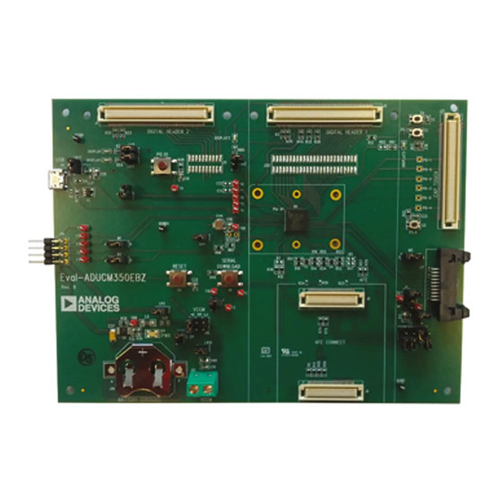
ADuCM350
motherboard
Selection of daughter boards for analog front end and
platform validation
3 power supply options: 2.5 V to 3.6 V from an external
power supply, 5 V from interface/emulator board, or
CR2032 battery connection
Interface options
UART and serial wire through 8-pin J-Link OB connector
Trace capability
Power indicator/general-purpose LEDs
Reset, download, and external interrupt push-buttons
Supercapacitor and thermistor capability
USB connectivity
8-pin connector to the interface/emulator board
Access to
ADuCM350
platform pins through Digital Header 1,
Digital Header2, and CapTouch header
32.768 kHz external crystal and 16 MHz external crystal
EVALUATION KIT CONTENTS
EVAL-ADuCM350EBZ
board
USB-SWD/UART-EMUZ, also known as J-Link OB emulator
AFE daughter boards:
ADuCM350
board,
ADuCM350
4-wire bio Configuration 2 board
ADuCM350
breakout board
ADuCM350
GPIO test header board
USB cable
USB-SWD/UART-EMUZ
PLEASE SEE THE LAST PAGE FOR AN IMPORTANT
WARNING AND LEGAL TERMS AND CONDITIONS.
ADuCM350
16-Bit, Precision, Low Power Meter-on-a-Chip
switch mux configuration
TYPICAL SETUP
PERIPHERALS
CONNECTOR
2
USB
CR2032
SUPPLY SUPPLY
Figure 1. Typical Setup (USB-SWD/UART-EMUZ on Left and
EVAL-ADuCM350EBZ User Guide
ADDITIONAL EQUIPMENT AND SOFTWARE NEEDED
Evaluation software for the
ADuCM350 design resources
Extra peripheral boards available for order: Ev-ADuCM350AUDZ,
Ev-ADuCM350DISZ
See the
ADuCM350 design resources
SYSTEM REQUIREMENTS
Minimum requirement to run examples and applications
PC with USB 2.0 controller connection and 1 free COM port
Windows XP SP3 or later, Windows Vista, or Windows 7 or later
ONLINE RESOURCES
Documents Needed
ADuCM350
data sheet
ADuCM350
hardware reference manual
AN-1262, AN-1263, AN-1271, AN-1281, AN-1286,
AN-1293,
ADuCM350
software development kit quick start guide
(UG-677)
Required Software
ADuCM350
software development kit (firmware/debug
environment)
IAR Embedded Workbench for ARM (from Version 7.10+)
ADuCM350
evaluation kit software platform (GUI software)
Design and Integration Files
Schematics, layout files, bill of materials
PERIPHERALS
CONNECTOR
1
AFE
DAUGHTER
BOARD
EXTERNAL
EVAL-ADuCM350EBZ
Rev. A | Page 1 of 28
ADuCM350
(download from the
page)
page for more details
AN-1302
application notes
CapTouch
CONNECTOR
TRACE
on Right)
UG-668
Advertisement
Table of Contents

Related Manuals for Analog Devices ADuCM350


Summary of Contents for Analog Devices ADuCM350
-
Page 1: Features
Evaluation software for the ADuCM350 (download from the Selection of daughter boards for analog front end and ADuCM350 design resources page) platform validation Extra peripheral boards available for order: Ev-ADuCM350AUDZ, 3 power supply options: 2.5 V to 3.6 V from an external... -
Page 2: Table Of Contents
ADuCM350 Daughter Board Schematics ........16 Revision History ................2 ADuCM350 Switch Mux Configuration Board ..... 16 General Description ................. 3 ADuCM350 4-Wire Bio Configuration 2 Board ....18 Getting Started .................. 4 Audio Daughter Board Reference Schematics ....... 20 Software Installation Procedures ..........4 Display Board Reference Schematics ........ -
Page 3: General Description
(EKSP)—both of which are available for excitation amplifier control loop to perform accurate potentiostat download on the ADuCM350 design resources page. type measurements and has a highly configurable switch matrix The software development kit is designed to work with the IAR that allows application specific amplifier configuration. -
Page 4: Getting Started
UG-668 EVAL-ADuCM350EBZ User Guide GETTING STARTED EVALUATION BOARD SETUP PROCEDURES SOFTWARE INSTALLATION PROCEDURES Plug the ADuCM350 switch mux configuration board into For software installation procedures, refer to the following ADuCM350 evaluation board, EVAL-ADuCM350EBZ. ADuCM350 software documentation for further details: Plug the USB-SWD/UART-EMUZ board into J14 on the •... -
Page 5: Evaluation Board Hardware
EVAL-ADuCM350EBZ User Guide UG-668 EVALUATION BOARD HARDWARE VDD_IO POWER SUPPLIES Table 2 describes the two options for supplying power to the VCCM_ANA VDD_IO pin. Table 1 describes the three options for supplying power to the VCCM_ANA pin. Table 2. VDD_IO Supply Options Link M5 Position VDD_IO Supply Table 1. -
Page 6: Jumper Settings
UG-668 EVAL-ADuCM350EBZ User Guide JUMPER SETTINGS Table 4. Link Option Functions Link Number Default Position Function Short AN_A to AFE daughter board. Open LED GPIO functionality of P2.1. Open AN_B to AFE daughter board. Short Connect the supercapacitor to the VBACK pin. Open Thermistor voltage output measurement (AN_A). -
Page 7: Evaluation Board Circuitry
J-LINK OB EMULATOR The J-Link OB emulator provides nonintrusive emulation via a serial wire and allows supply and UART communication with ADuCM350 evaluation board (EVAL-ADuCM350EBZ). Figure 4 shows a top view of the emulator board. The J2 connector plugs into the... -
Page 8: Digital Header Pad Lookup Table
UG-668 EVAL-ADuCM350EBZ User Guide DIGITAL HEADER PAD LOOKUP TABLE Table 5. Pinout for Digital Header 1 Pad (J20) on EVAL-ADuCM350EBZ Top Row (from Left to Right) Bottom Row (from Left to Right) Pin No. Internal Connection Pin No. Internal Connection J20-2 P2.1 J20-1... -
Page 9: Aducm350 Motherboard Schematics
EVAL-ADuCM350EBZ User Guide UG-668 ADUCM350 MOTHERBOARD SCHEMATICS ADuCM350 P0.0 P0.0 P0.1 P0.1 P0.2 P0.2 P0.3 P0.3 P0.4 KERNEL_GPIO P0.4 KERNEL_GPIO P0.5 P0.5 APLATFORM_TEST P0.6 RESETX P0.6 RESETX P0.7 ADUCM350-OM P0.7 P0.8 P0.8 P0.9 P0.9 P0.10 VREF P0.10 VREF P0.11 VBIAS P0.11... - Page 10 UG-668 EVAL-ADuCM350EBZ User Guide LF 32kHz XTAL HF 16MHz XTAL DISPLAY2 DISPLAY VCCM_DIG 3.3V_BOARD P2.1 P0.11 560 r 560 r LED-0603 -RED LED-0603 -RED HF_XTAL1 HF_XTAL2 RTC_XTAL1 15pF DISPLAY3 DISPLAY1 3.3V_BOARD 3.3V_BOARD LK12 P3.6 P4.2 560 r 560 r LED-0603 -RED LED-0603 -RED XTAL-FA238 24pF...
- Page 11 EVAL-ADuCM350EBZ User Guide UG-668 Figure 9. Digital Schematics 2 Rev. A | Page 11 of 28...
- Page 12 UG-668 EVAL-ADuCM350EBZ User Guide Figure 10. Analog Schematics 1 Rev. A | Page 12 of 28...
- Page 13 EVAL-ADuCM350EBZ User Guide UG-668 THERMISTOR 3.3V_BOARD REF_EXCITE_1 REF_EXCITE 22.6K These can be re-arranged to suit Layout AN_A P0-1 100pF P0.1 AGND P0-0 P0.0 P0-2 P0.2 P0-3 UNCOMITTED INPUTS - CONNECTORS. P0.3 LK11 AN_D_1 P0-5 AN_C_1 P0.5 AN_B_1 P0-4 AN_A_1 P0.4 CONNECTOR STANDARD AN_A...
- Page 14 UG-668 EVAL-ADuCM350EBZ User Guide Figure 12. Interface Rev. A | Page 14 of 28...
- Page 15 EVAL-ADuCM350EBZ User Guide UG-668 Figure 13. Power Rev. A | Page 15 of 28...
-
Page 16: Aducm350 Daughter Board Schematics
UG-668 EVAL-ADuCM350EBZ User Guide ADUCM350 DAUGHTER BOARD SCHEMATICS ADUCM350 SWITCH MUX CONFIGURATION BOARD MOTHERBOARD CONNECTOR—ALIGN J8 AND J9. J9-1 J9-21 J9-41 AFE1 J8-1 J8-21 J8-41 AN_A_1 J9-2 J9-22 J9-42 AFE6 J8-2 J8-22 J8-42 VCCM_ANA J9-3 J9-23 J9-43 P4.2 J8-3 J8-23... - Page 17 EVAL-ADuCM350EBZ User Guide UG-668 AFE1 AFE2 AFE3 LK19 LK20 AFE4 AFE5 LK21 LK22 AFE6 AFE7 AFE8 Figure 15. Switch Mux Configuration—Sensor Hookup Rev. A | Page 17 of 28...
-
Page 18: Aducm350 4-Wire Bio Configuration 2 Board
UG-668 EVAL-ADuCM350EBZ User Guide ADUCM350 4-WIRE BIO CONFIGURATION 2 BOARD MOTHERBOARD CONNECTOR—ALIGN J8 AND J9. J9-1 J9-21 J9-41 AFE1 J8-1 J8-21 J8-41 AN_A_1 J9-2 J9-22 J9-42 AFE6 J8-2 J8-22 J8-42 VCCM_ANA J9-3 J9-23 J9-43 P4.2 J8-3 J8-23 J8-43 AN_B_1 J9-4... - Page 19 EVAL-ADuCM350EBZ User Guide UG-668 RCAL TEST POINTS TP12 RCAL2 M20-9991246 Harwin 3.3V_BOARD J1-4 M20-9991246 Harwin REF_EXCITE_1 J1-1 M20-9991246 Harwin VBIAS_1 J1-5 M20-9991246 RCAL1 Harwin VREF_1 J1-6 M20-9991246 Harwin VCCM_ANA J1-12 M20-9991246 Harwin P0.10 J1-3 M20-9991246 Harwin P4.2 J1-2 IV GAIN TP10 TIA_I M20-9991246...
-
Page 20: Audio Daughter Board Reference Schematics
UG-668 EVAL-ADuCM350EBZ User Guide AUDIO DAUGHTER BOARD REFERENCE SCHEMATICS The Figure 19 schematic is connected to Digital Header 2 (J1) on the EVAL-ADuCM350EBZ board. BEEPER AND I2S AMPLIFIER PINOUT STANDARD P3.12 CONNECTOR BEEPER P3.13 BEEP - P3.12 P3.14 BEEPX - P3.1 P4.0 P4.1 MCLK - P3.12... - Page 21 EVAL-ADuCM350EBZ User Guide UG-668 Figure 20 is a reference schematic both for the beeper/piezoelectric buzzer setup and for the I S setup using the SSM2518. J2-1 Ext PVD PVDD BUZZER 0.1uF J2-2 BEEP SELECTOR DIODE-BAS40DW-04 PVDD PKLCS1212E4001 0.1uF 4.7uF BEEP DVDD PVDD PVDD...
-
Page 22: Display Board Reference Schematics
UG-668 EVAL-ADuCM350EBZ User Guide DISPLAY BOARD REFERENCE SCHEMATICS The Figure 21 schematic is the connector to Digital Header 1 (J6) on the EVAL-ADuCM350EBZ board. DISPLAY/PDI HEADER P0.12 J1-1 J1-120 P2.0 J1-2 J1-119 P0.13 J1-3 J1-118 VUSB P2.1 J1-4 J1-117 J1-5 J1-116 P2.2 J1-6... - Page 23 EVAL-ADuCM350EBZ User Guide UG-668 TFT Display Reference Schematic The schematic shown in Figure 22 is used to connect to an INT035TFT or INT035TFT-TS thin film transistor LCD module from Displaytech Ltd. 3.3V_BOARD VDD_IO LCD_MODULE_SINT035TFT VLCD_VDD VDDIO VDDD VDDLCD TP_AUX TP_TIRQ TP_DIN TP_CLK TP_DOUT...
- Page 24 UG-668 EVAL-ADuCM350EBZ User Guide LCD Segment Display Reference Schematic The schematic shown in Figure 23 is used to connect to a VIM-828 LCD segment display from Varitronix. CONNECTOR FOR VIM-828 - TO DISCUSS VIM-828 P2.3 COM3_P2.3 P2.4 S1_P2.4 P2.5 S2_P2.5 P1.0 S3_P1.0 P1.1...
-
Page 25: Breakout Board Pin Connections
EVAL-ADuCM350EBZ User Guide UG-668 BREAKOUT BOARD PIN CONNECTIONS If using the ADuCM350 breakout board, the connections shown in Figure 24 and Figure 25 are required. P0.13 P0.14 P0.15 P3.12 P3.13 P3.14 P4.0 P4.1 VCCM_ANA P4.2 VCCM_ANA P0.10 3.3V_BOARD P0.11 3.3V_BOARD P0.12... -
Page 26: Gpio Test Header Board
UG-668 EVAL-ADuCM350EBZ User Guide GPIO TEST HEADER BOARD The Figure 26 schematic is the connector to Digital Header 1 (J6) on the EVAL-ADuCM350EBZ board. DIGITAL HEADER 1 J6-1 J6-120 P2.0 J6-2 J6-119 J6-3 J6-118 P2.1 J6-4 J6-117 J6-5 J6-116 P2.2 J6-6 J6-115 J6-7... - Page 27 EVAL-ADuCM350EBZ User Guide UG-668 3.3V_BOARD TP0_5 3.3V_BOARD P0_5_ TP0_4 P0_4_ 560r P0.5 P0.4 560r P0_5 P0_4 0.1uF 0.1uF DGND1 DGND2 3.3V_BOARD TP3_4 P3_4_ P3.4 3.3V_BOARD 560r TP3_6 P3_6 P3.6 P3_4 560r 0.1uF TP3_1 560r P3.1 3.3V_BOARD TP3_2 560r P3.2 3.3V_BOARD DGND3 TP3_3 P0_0...
-
Page 28: Limitations On Use And Liability
By using the evaluation board discussed herein (together with any tools, components documentation or support materials, the “Evaluation Board”), you are agreeing to be bound by the terms and conditions set forth below (“Agreement”) unless you have purchased the Evaluation Board, in which case the Analog Devices Standard Terms and Conditions of Sale shall govern. Do not use the Evaluation Board until you have read and agreed to the Agreement.
Need help?
Do you have a question about the ADuCM350 and is the answer not in the manual?
Questions and answers