Table of Contents
Advertisement
UM2525
User manual
Evaluation boards with STM32H747XI and STM32H757XI MCUs
Introduction
The
STM32H747I-EVAL
and
STM32H757I-EVAL
Evaluation boards (STM32H7x7I-EVAL) are high-end development platforms
®
®
for the Arm
Cortex
-M7-based
STM32H747XI
and
STM32H757XI
microcontrollers (STM32H7x7XI), respectively. The
STM32H7x7I-EVAL Evaluation boards provide access to all the STM32 peripherals for user applications, and include an
embedded STLINK-V3E debugger/programmer.
The full range of the STM32H7x7I-EVAL hardware features helps develop applications and evaluate all peripherals: USB
OTG_HS and FS, Ethernet, FDCAN, USART, Audio DAC and ADC, digital microphone, SRAM, SDRAM, NOR Flash memory,
™
Twin Quad-SPI Flash memory, microSD
3.0 card, 4" 480×800 TFT color LCD with MIPI DSI
SM
interface and capacitive
touchpanel, and cryptographic hardware accelerator (available only on
STM32H757XI
devices) .
The expansion connectors provide an easy way to add specialized features, while ETM trace is supported through external
probes.
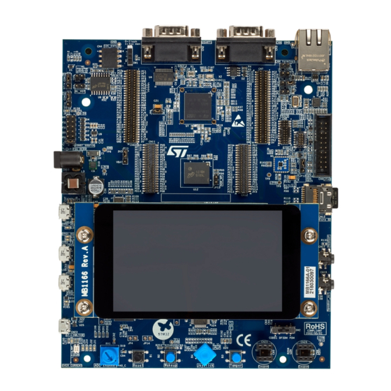
Figure 1.
STM32H7x7I-EVAL board (top view)
Picture is not contractual.
UM2525 - Rev 3 - May 2019
www.st.com
For further information contact your local STMicroelectronics sales office.
Advertisement
Table of Contents

Subscribe to Our Youtube Channel
Related Manuals for ST STM32H757I-EVAL


Summary of Contents for ST STM32H757I-EVAL
-
Page 1: Figure 1. Stm32H7X7I-Eval Board (Top View)
UM2525 User manual Evaluation boards with STM32H747XI and STM32H757XI MCUs Introduction STM32H747I-EVAL STM32H757I-EVAL Evaluation boards (STM32H7x7I-EVAL) are high-end development platforms ® ® for the Arm Cortex -M7-based STM32H747XI STM32H757XI microcontrollers (STM32H7x7XI), respectively. The STM32H7x7I-EVAL Evaluation boards provide access to all the STM32 peripherals for user applications, and include an embedded STLINK-V3E debugger/programmer. -
Page 2: Features
JTAG/SWD and ETM trace – Extension connectors and memory connectors for daughterboard or wire-wrap board • Flexible power-supply options: ST-LINK USB V or external sources • On-board STLINK-V3E debugger/programmer with USB re-enumeration capability: mass storage, Virtual COM port, and debug port •... -
Page 3: Ordering Information
Evaluation tools marked as “ES” or “E” are not yet qualified and therefore not ready to be used as reference design or in production. Any consequences deriving from such usage will not be at ST charge. In no event, ST will be liable for any customer usage of these engineering sample tools as reference design or in production. -
Page 4: Development Environment
STM32 Flash memory for easy demonstration of the device peripherals in standalone mode. The latest versions of the demonstration source code and associated documentation can be downloaded from www.st.com. UM2525 - Rev 3 page 4/69... -
Page 5: Conventions
UM2525 Conventions Conventions Table 3 provides the conventions used for the ON and OFF settings in the present document. Table 3. ON/OFF convention Convention Definition Jumper JPx ON Jumper fitted Jumper JPx OFF Jumper not fitted Jumper JPx [1-2] Jumper should be fitted between Pin 1 and Pin 2 Solder bridge SBx ON SBx connections closed by 0 Ω... -
Page 6: Delivery Recommendations
UM2525 Delivery recommendations Delivery recommendations Some verifications are needed before using the Evaluation board for the first time, to make sure that no damage occurred during shipment and that no components are unplugged or lost. When the board is extracted from its plastic bag, check that no component remains in the bag. The main component to verify is the microSD card that may have been ejected from the connector CN13 (right side of the board). -
Page 7: Stm32H7X7I-Eval Hardware Layout And Configuration
STM32H7x7XIH6U and illustrates the connection between the microcontroller and the peripherals (SDRAM, SRAM, NOR Flash, Twin Quad-SPI Flash, color LCD, USB OTG connectors, USART, Ethernet, Audio, FDCAN, microSD 3.0 card and embedded ST-LINK). Figure 3. STM32H7x7I-EVAL Evaluation board (top side) helps users to locate these features on the Evaluation board. - Page 8 USB OTG1 CN20 LCD Connector CN16 USB OTG1 FS CN17 Headset CN18 Audio jack USB OTG2 CN19 Speaker out jack CN23 ST-LINK/V3E LD11 STLINK-V3E Power U26 (CN26) overcurrent Right Digital Alarm Microphone LD12 (Coupon ST-LINK/V3E U27 (CN25) connectors) COM LED...
-
Page 9: Stm32H753I-Eval Evaluation Board Mechanical Drawing
UM2525 Ordering information Ordering information Figure 4 Table 4 show the mechanical dimensions for the MB1246 board with the 5.7” LCD daughterboard. Figure 4. STM32H7x7I-EVAL Evaluation board mechanical drawing Table 4. Mechanical dimensions Symbol Size(mm) Symbol Size(mm) Symbol Size(mm) 68.58 16.76 48.62 13.7... -
Page 10: Embedded St_Link/V2-1
The STLINK-V3E requires drivers to be installed on Windows . It embeds a firmware which needs to be updated from time to time to benefit from new functionalities and bug corrections. Refer to technical note "Overview of ST- LINK derivated" (TN1235) for details. -
Page 11: Table 5. Power Related Jumpers
The STM32H7x7I-EVAL Evaluation board can be powered from the STLINK-V3E USB connector CN23 (U5V), but only the ST-LINK/V2-1 circuit has the power before USB enumeration, because the host PC only provides 100 mA to the board at that time. During the USB enumeration phase the STM32H7x7I-EVAL board requires 300 mA power from the host PC. - Page 12 UM2525 Power supply Jumper Description JP10 is used to select one of the six possible power supply resources. To supply the STM32H7x7I-EVAL board through the USB connector of the STLINK-V3E (CN23) set JP10 as shown below: (default setting) STlk To supply the STM32H7x7I-EVAL board through the jack (CN10), set JP10 as shown below: STlk To supply the STM32H7x7I-EVAL board through the daughterboard connectors (CN6 and CN7), set JP10 as shown below:...
- Page 13 UM2525 Power supply Jumper Description To supply the STM32H7x7I-EVAL board through the USB OTG1_HS (CN14), set JP10 as shown below: STlk JP10 To supply the STM32H7x7I-EVAL board and the daughterboard connected on CN6 and CN7 through the power supply jack (CN10), set JP10 as shown below (daughterboard must not have its power supply connected) STlk is connected to +3.3 V when JP11 is set as shown below: (Default setting) JP11...
-
Page 14: Smps/Ldo Power Supply
Resolder the solder bridges as described above for SMPS or LDO mode. At power-on, check that the ST-LINK operates normally. When the ST-LINK is connected, use the right SMPS/LDO configuration for your application. Clock source Two clock sources (X1 and X2) are available on the STM32H7x7I-EVAL Evaluation board for the STM32H7x7XI, and embedded RTC. -
Page 15: Reset Sources
ST programmed value: Flash at 0x0800 0000. CPU boot address defined by user option byte BOOT_ADD1 BOOT_ADD1[15:0] [15:0] ST programmed value: System boot loader at 0x0000 0000. Table 9. Boot related jumpers Jumper Description The Bootloader_BOOT0 is managed by pin 6 of connector CN2 (RS232 DSR signal) when JP3 is ON. This configuration is used for boot-loader application only. -
Page 16: Audio
SW2 shown in Table 10. Audio related switch and jumper. The coupon connectors CN25 and CN26 can be used to support ST-MEMS microphone STEVAL-MKI129V1 after removing SB54 and SB55 solder bridges. Table 10. Audio related switch and jumper... -
Page 17: Usb Otg2 Hs And Fs
UM2525 USB OTG2_FS The Evaluation board can be powered by these USB connectors (CN14 or CN16) at 5 V DC with 500 mA current limitation. As several OTG1_FS signals are shared with the OTG1_HS ULPI bus and USART1, some PCB reworks are needed when using OTG1_FS (CN16) as shown in Table Table 11. -
Page 18: Microsd ™ Card
UM2525 microSD™ card Table 12. USART1 related jumpers Jumper Description USART1_TX is connected to RS232 when JP7 is set as shown below (Default setting): USART1_TX is connected to the USART_RX of the STLINK-V3E controller when JP7 is set as shown below: USART1_RX is connected to RS232 when JP8 is set as shown below (Default setting): USART1_RX is connected to the USART_TX of the STLINK-V3E controller when JP8 is set as shown below: 6.12... -
Page 19: Memories
UM2525 Memories Table 14. Ethernet related jumpers Jumper Description 50M RMII reference clock is generated by an external crystal X3 when JP5 is set as shown below: (Default setting) 50M RMII reference clock is generated by MCO at PA8 when JP5 is set as shown below: 6.16 Memories An 8M x 32-bit SDRAM is connected to the SDRAM bank1 of the FMC interface of the STM32H7x7XI... -
Page 20: Display And Input Devices
UM2525 Display and input devices 6.19 Display and input devices Four general-purpose-color LEDs (LD 1, 2, 3 and 4) are available as display device. The 4-direction joystick (B4) with selection, Wakeup (B2) and Tamper/key button (B3) are available as input devices. -
Page 21: Mfx (Multifunction Expander)
UM2525 MFX (multifunction eXpander) 6.20 MFX (multifunction eXpander) MFX circuit on STM32H7x7I-EVAL Evaluation board acts as IO-expander. The communication interface between MFX and STM32H7x7XI is I2C1 bus. The signals connected to MFX are listed in Table 17. MFX signals. Table 17. MFX signals Direction Pin number of MFX Pin name of MFX MFX functions... -
Page 22: Stm32H7X7I-Eval Connectors
UM2525 STM32H7x7I-EVAL connectors STM32H7x7I-EVAL connectors Ethernet RJ45 connector CN1 Figure 5. Ethernet RJ45 connector CN1 (front view) Table 18. RJ45 connector CN1 Pin number Description Pin number Description TxData+ TxData- RxData+ Shield Shield RxData- Shield Shield RS232 connector CN2 Figure 6. RS232 connector CN2 (front view) Table 19. -
Page 23: Can D-Type, 9-Pin Male Connector Cn3
UM2525 CAN D-type, 9-pin male connector CN3 CAN D-type, 9-pin male connector CN3 Figure 7. CAN D-type, 9-pin connector CN3 (front view) Table 20. CAN D-type 9-pin male connector CN3 Pin number Description Pin number Description 1,4,8,9 CANH CANL 3,5,6 External I C connector CN4 Figure 8. -
Page 24: Daughterboard Extension Connector Cn6 And Cn7
CN11 and CN12. The space between these two connectors is defined as a standard that allows developing common daughterboards for several ST evaluation boards. The standard width between CN6 pin1 and CN7 pin1 is 2700 mils (68.58 mm). Each pin on CN6 and CN7 can be used by a daughterboard after disconnecting it from the corresponding function block on STM32H7x7I-EVAL Evaluation board. - Page 25 UM2525 Daughterboard extension connector CN6 and CN7 Pin Description Alternate function How to disconnect with function block on STM32H7x7I-EVAL board DFSDM_DATA1 Not to dial SW2 to the middle PB14 USART1_TX/USB_FS1_DM Open SB46, SB47 PB15 USART1_RX/USB_FS1_DP Open SB49, SB51 PB11 ULPI_D4 Remove R108 TRGIN Remove SB24...
- Page 26 UM2525 Daughterboard extension connector CN6 and CN7 Pin Description Alternate function How to disconnect with function block on STM32H7x7I-EVAL board PJ10 Table 24. Daughterboard extension connector CN7 How to disconnect with function block on STM32H7x7I-EVAL Pin Description Alternate function board PF10 GPIO_DSI_RST Remove R286, Disconnect CN15...
-
Page 27: Etm Trace Debugging Connector Cn8
UM2525 ETM trace debugging connector CN8 How to disconnect with function block on STM32H7x7I-EVAL Pin Description Alternate function board GPIO_EXPANDER_INT Remove R185 SDIO_1_CDIR Add R139 10Kohm, Remove R91 I2C_1_SDA Remove R160, R181, R209, Disconnect CN4, CN15 I2C_1_SCL Remove R155, R180, R212, Disconnect CN4, CN15 NJTRST Remove R79 LED3... -
Page 28: Jtag/Swd Connector Cn9
UM2525 JTAG/SWD connector CN9 Table 25. ETM trace debugging connector CN8 Pin number Description Pin number Description +3.3V TMS/PA13 TCK/PA14 TDO/PB3 TDI/PA15 RESET# TraceCLK/PE2 TraceD0/PE3 or SWO/PB3 TraceD1/PE4 or nTRST/PB4 TraceD2/PE5 TraceD3/PE6 JTAG/SWD connector CN9 Figure 11. JTAG/SWD debugging connector CN9 (top view) Table 26. -
Page 29: Power Connector Cn10
UM2525 Power connector CN10 Power connector CN10 The STM32H7x7I-EVAL Evaluation board can be powered from a DC 5 V power supply through the external power supply jack (CN10) shown in Figure 13. Power supply connector CN10 (front view). The central pin of CN10 must be positive. -
Page 30: Table 28. Memory Connector Cn12
UM2525 Memory connector CN11 and CN12 Description Alternative function How to disconnect with function block on STM32H7x7I-EVAL board PD14 SDNWE PF14 PF11 SDNRAS PE11 PF15 PE14 PH10 A14/BA0 PH12 PD10 PD15 SDCLK Table 28. Memory connector CN12 How to disconnect with function block on Pin Description Alternative function STM32H7x7I-EVAL board... - Page 31 UM2525 Memory connector CN11 and CN12 How to disconnect with function block on Pin Description Alternative function STM32H7x7I-EVAL board NBL0 PG10 PH13 SDCKE1 A21/SAI1_SCK_A/TRACED2 Open SB41, SB42 NWAIT A23/PDM1_CK1/ SAI1_MCLK_A /TRACECLK Open SB11, SB15, SB57 PH15 PH14 +3.3V UM2525 - Rev 3 page 31/69...
-
Page 32: Microsd Connector Cn13
UM2525 microSD™ connector CN13 7.11 ™ microSD connector CN13 ™ Figure 13. microSD connector (top view) Table 29. microSD connector CN13 Pin number Description Pin number Description SD_DATA2 Vss/GND SD_DATA3 SD_DATA0 SD_CMD SD_DATA1 +2.9V_SD MicroSDcard_detect SD_CLK (MFX GPIO15) 7.12 USB OTG1_HS Micro-AB connector CN14 Figure 14. -
Page 33: Tft Lcd Connector Cn15
UM2525 TFT LCD connector CN15 Table 30. USB OTG1_HS Micro-AB connector CN14 Pin number Description Pin number Description 7.13 TFT LCD connector CN15 A TFT-color LCD with MIPI DSI interface board is mounted on CN15. Refer to Section 6.19 Display and input devices for details. -
Page 34: Audio Jack (Speaker) Cn19
UM2525 Audio jack (speaker) CN19 Table 32. USB OTG2_FS Micro-AB connector CN18 Pin number Description Pin number Description (PA9) ID (PA10) D- (PA11) D+ (PA12) 7.17 Audio jack (speaker) CN19 A 3.5mm stereo audio jack CN19 for speaker out is available on STM32H7x7I-EVAL Evaluation board to support an external speaker. -
Page 35: Mems Microphone Coupon Connectors Cn25 And Cn26
UM2525 STDC14 debugging connector CN24 7.21 STDC14 debugging connector CN24 Figure 18. STDC14 debugging connector CN24 (top view) Table 34. STDC14 debugging connector CN24 Pin number Description Pin number Description +3.3V SWDIO-TMS /PA13 SWCLK-TCK /PA14 SWO-TDO/PB3 TDI/PA15 GNDDetect RESET# VCP_USART_RX /PB14 VCP_USART_TX /PB15 7.22 MEMS microphone coupon connectors CN25 and CN26... - Page 36 UM2525 MEMS microphone coupon connectors CN25 and CN26 Pin number Description Pin number Description UM2525 - Rev 3 page 36/69...
-
Page 37: Stm32H7X7I-Eval I/O Assignment
UM2525 STM32H7x7I-EVAL I/O assignment STM32H7x7I-EVAL I/O assignment Table 36. STM32H7x7I-EVAL I/O assignment Pin number Pin name Default function Alternate function PA0-WKUP KEY_WKUP0 RMII_REF_CLK RMII_MDIO ULPI_D0 EXT_RESET ULPI_CK GPIO_LCD_BACKLIGHT_CTRL RMII_CRS_DV MCO1 USB_FS2_VBUS PA10 USB_FS2_ID PA11 USB_FS2_DM FDCAN_1_RXFD PA12 USB_FS2_DP FDCAN_1_TXFD PA13 JTMS-SWDIO PA14 JTCK-SWCLK... - Page 38 UM2525 STM32H7x7I-EVAL I/O assignment Pin number Pin name Default function Alternate function RMII_RXD1 SDIO_1_D0DIR SDIO_1_D123DIR SDIO_1_D0 SDIO_1_D1 PC10 SDIO_1_D2 PC11 SDIO_1_D3 PC12 SDIO_1_CK PC13-ANTI_TAMP KEY_TAMP_1/WKUP2 PC14-OSC32_IN OSC32_IN PC15-OSC32_OUT OSC32_OUT FMC_D2 FMC_D3 SDIO_1_CMD GPIO_CAN_STANDBY FMC_NOE FMC_NWE FMC_NWAIT FMC_NE1 FMC_D13 FMC_D14 PD10 FMC_D15 PD11 FMC_A16...
- Page 39 UM2525 STM32H7x7I-EVAL I/O assignment Pin number Pin name Default function Alternate function PE13 FMC_D10 PE14 FMC_D11 PE15 FMC_D12 FMC_A0 FMC_A1 FMC_A2 FMC_A3 FMC_A4 FMC_A5 QSPI_BK1_IO3 QSPI_BK1_IO2 QSPI_BK1_IO0 QSPI_BK1_IO1 PF10 GPIO_DSI_RST PF11 SDR_SDNRAS PF12 FMC_A6 PF13 FMC_A7 PF14 FMC_A8 PF15 FMC_A9 FMC_A10 FMC_A11 FMC_A12...
- Page 40 UM2525 STM32H7x7I-EVAL I/O assignment Pin number Pin name Default function Alternate function SDR_SDNWE SDR_SDNE1 SDR_SDCKE1 FMC_D16 FMC_D17 PH10 FMC_D18 PH11 FMC_D19 PH12 FMC_D20 PH13 FMC_D21 PH14 FMC_D22 PH15 FMC_D23 FMC_D24 FMC_D25 FMC_D26 FMC_D27 FMC_NBL2 FMC_NBL3 FMC_D28 FMC_D29 PI8- ANTI TAMP2 GPIO_EXPANDER_INT FMC_D30 PI10...
- Page 41 UM2525 STM32H7x7I-EVAL I/O assignment Pin number Pin name Default function Alternate function PJ13 PJ14 PJ15 LED1 LED2 LED3 LED4 PA0_C Potentiometer PA1_C PC2_C PC3_C UM2525 - Rev 3 page 41/69...
-
Page 42: Stm32H7X7I-Eval Electrical Schematics
UM2525 STM32H7x7I-EVAL electrical schematics STM32H7x7I-EVAL electrical schematics This section provides the design schematics for the STM32H7x7I-EVAL Evaluation board: • Overall schematic for the STM32H7x7I-EVAL (see Figure • STM32H7x7I-EVAL MCU (see Figure • Power (see Figure • SRAM, Flash memory and SDRAM (see Figure •... -
Page 43: Figure 20. Stm32H7X7I-Eval Evaluation Board
Figure 20. STM32H7x7I-EVAL Evaluation board U_MCU U_Memory MCU.SchDoc Same length Memory.SchDoc R212 +3V3 I2C1_SCL A[0..23] A[0..23] R209 I2C1_SDA D[0..31] D[0..31] U_Audio 90MHz clock SDCLK SDCLK Audio.SchDoc SDNE1 SDNE1 I2C1_SCL SAI1_SCKA SAI1_SCKA SDNRAS SDNRAS I2C1_SDA SAI1_FSA SAI1_FSA SDNCAS SDNCAS SAI1_SDA SAI1_SDA SDNWE SDNWE SAI1_SDB... -
Page 44: Figure 21. Stm32H7X7I-Eval Mcu
Figure 21. STM32H7x7I-EVAL MCU R265 R256 WAKEUP R262 R264 RMII_REF_CLK R270 R263 ETH_MDIO SDIO1_CMD ULPI_D0 R260 R267 LED3_RGB FDCAN1_STBY R261 EXT_RESET FMC_NOE FMC_NBL2 SB62 Closed R272 ULPI_CK FMC_NWE ETH_nINT FMC_NBL3 R259 R243 LCD_BL_CTRL FMC_NWAIT QSPI_BK1_NCS SAI1_MCLKA SB56 Open R240 RMII_CRS_DV FMC_NE1 R268 SDCLK... -
Page 45: Figure 22. Stm32H7X7I-Eval Power
Figure 22. STM32H7x7I-EVAL power VDD_MCU Power configurations: ZEN056V130A24LS Mode Mount Removed CN10 LDO mode SB14,SB16,SB20 STM32H7x3 SB13,SB23,SB18 SB10,SB17,SB53 Default setting 220uF SMPS mode SB14,SB20,SB10 SB13,SB17,SB23 DC-10B STM32H7x7 SB53 SB16,SB18 SMAJ5.0A-TR Default setting SMPS+LDO SB13,SB23,SB10 SB14,SB16,SB17 100nF BNX002-01 mode SB53, SB18,SB20 VDD_MCU JP10 BEAD(FBMJ1608HM180NTR) -
Page 46: Figure 23. Stm32H7X7I-Eval Sram, Flash And Sdram
Figure 23. STM32H7x7I-EVAL SRAM, FLASH and SDRAM D[0..31] D[0..31] A[0..23] A[0..23] DQ31 DQ30 I/O15 DQ15A-1 DQ29 I/O14 DQ14 DQ28 I/O13 DQ13 DQ27 I/O12 DQ12 DQ26 I/O11 DQ11 DQ25 I/O10 DQ10 DQ24 I/O9 DQ23 I/O8 DQ22 I/O7 DQ21 I/O6 DQ20 I/O5 DQ19 I/O4 DQ18... -
Page 47: Figure 24. Stm32H7X7I-Eval Audio
Figure 24. STM32H7x7I-EVAL audio +3V3 LDO1VDD AGND Default I2C Address:0011010 +3V3 AVDD1 AGND SPKVDD1 AGND +1V8 SPKVDD2 SPKGND1 AVDD2 SPKGND2 +1V8 CPVDD CPGND +3V3 DCVDD DGND DBVDD HP2GND +1V8 LDO2VDD R160 I2C1_SDA R157 R155 +3V3 LDO1ENA SCLK I2C1_SCL R163 [N/A] LDO2ENA CS/ADDR +3V3... -
Page 48: Figure 25. Stm32H7X7I-Eval Lcd Connectors
Figure 25. STM32H7x7I-EVAL LCD connectors DSI LCD RGB LCD CN20 LCD_R[0..7] PI15 LCD_R0 LCD_G0 LCD_G[0..7] LCD_R[0..7] LCD_G[0..7] LCD_R1 LCD_G1 LCD_R2 LCD_G2 LCD_R3 LCD_G3 PJ10 LCD_R4 LCD_G4 PJ11 11 12 LCD_R5 LCD_G5 13 14 CN15 LCD_R6 LCD_G6 15 16 LCD_R7 LCD_G7 17 18 To MFX 19 20... -
Page 49: Figure 26. Stm32H7X7I-Eval Ethernet
Figure 26. STM32H7x7I-EVAL Ethernet +3V3 BEAD 100nF +3V3 I/O1 I/O4 Vbus I/O2 I/O3 C102 USBLC6-4SC6 100nF Diff Pair 100ohm TD_P Diff Pair 100ohm PG11 TD_N RMII_TX_EN TXEN PG13 RMII_TXD0 TXD0 PG12 RD_P RMII_TXD1 TXD1 RD_N RMII_RXD0 RXD0/MODE0 Diff Pair 100ohm RMII_RXD1 RXD1/MODE1 LED1/nINT/nPME/REGOFF... -
Page 50: Figure 27. Stm32H7X7I-Eval Usb Otg_Hs
Figure 27. STM32H7x7I-EVAL USB OTG_HS +3V3 ESDA7P60-1U1M R289 CN16 PB13 VBUS_FS1 VBUS PB14 USB_FS1_DM PB15 USB_FS1_DP PB12 USB_FS1_ID Green I/O1 I/O4 Shield Vbus Shield R135 I/O2 I/O3 Shield 9013 Shield USBLC6-4SC6 475900001 R137 +3V3 R126 MFX_GPIO8 R287 OTG_FS1_OverCurrent SB28 +3V3 To MFX R125 MFX_GPIO9... -
Page 51: Figure 28. Stm32H7X7I-Eval Usb Otg_Fs
Figure 28. STM32H7x7I-EVAL USB OTG_FS +3V3 R290 MFX_GPIO6 OTG_FS2_OverCurrent R144 To MFX R146 CN18 FAULT VBUS MFX_GPIO7 R141 OTG_FS2_PowerSwitchOn From MFX STMPS2151STR 4.7uF R140 Shield Shield Shield Shield 475900001 +3V3 VBUS_FS2 PA11 USB_FS2_DM PA12 USB_FS2_DP PA10 R165 USB_FS2_ID I/O1 I/O4 Vbus LD10 I/O2... -
Page 52: Figure 29. Stm32H7X7I-Eval Rs232
Figure 29. STM32H7x7I-EVAL RS232 +3V3 C104 C101 100nF 100nF DB9-male USART1 C105 100nF 100nF 100nF T1IN T1OUT PB14 RS232_TX T2IN T2OUT T3IN T3OUT R1OUTB Bootloader_BOOT0 R2OUTB R1OUT R1IN R2OUT R2IN PB15 RS232_RX R3OUT R3IN Bootloader_RESET R4OUT R4IN R5OUT R5IN +3V3 nSHDN ST3241EBPR RS232... -
Page 53: Figure 30. Stm32H7X7I-Eval Fdcan And Qspi
Figure 30. STM32H7x7I-EVAL FDCAN and QSPI FDCAN C100 FDCAN1_STBY DB9-male CAN connector Default setting: Open 100nF PA12 FDCAN1_TX STBY CANH CANL PA11 FDCAN1_RX +3V3 MCP2562FD 100nF ESDCAN02-2BWY R213 R214 [N/A] +3V3 Twin Quad SPI Flash QSPI_CLK BK2_IO3 QSPI_CLK QSPI_BK1_IO3 HOLD_1#/DQ3 CLK_1 QSPI_CLK HOLD#/DQ3... -
Page 54: Figure 31. Stm32H7X7I-Eval Microsd 3.0 Card
Figure 31. STM32H7x7I-EVAL microSD 3.0 card MICRO SD 3.0 Card +3V3 R112 R115 R110 [N/A] [N/A] [N/A] [N/A] [N/A] +2V9_SD Module board PC12 SDIO1_CLK CLK_IN DATA0_SD R161 SDIO1_CKIN CLK_FB DATA1_SD DATA2_SD SDIO1_CMD CMD_H DATA3_SD SDIO1_CDIR DIR_CMD CLK_SD CMD_SD SDIO1_D0 DATA0_H SDIO1_D1 DATA1_H PC10... -
Page 55: Figure 32. Stm32H7X7I-Eval Peripherals
Figure 32. STM32H7x7I-EVAL peripherals Buttons Potentiometer +3V3 +3V3 R205 R194 Two pin header for external analog input +3V3 R193 PC13 TAMPER_KEY WKUP [N/A] PA0_C Potentiometer USER (Blue) R11 0 100nF ESDALC6V1-1U2 100nF 3386P-103(10K) R203 WAKEUP [N/A] R192 R204 220K Wakeup Button ESDALC6V1-1U2 Tamper &... -
Page 56: Figure 33. Stm32H7X7I-Eval Extension Connectors
Figure 33. STM32H7x7I-EVAL extension connectors Place close Memory CN11 SDNE1 SDNWE PF13 PF14 PF12 PF11 SDNRAS SB39 Left Right Open PF10 11 12 SB40 PC15 PC14 PE10 13 14 R215 Open PI14 PI12 Open PE12 PE11 RESET# 15 16 PI11 Open PI13 PE15... -
Page 57: Figure 34. Stm32H7X7I-Eval Stlink-V3E
Figure 34. STM32H7x7I-EVAL STLINK-V3E RED 2V R195 5 Volts ST-LINK CN21 U23A LD11 R142 Fitted: NO VUSB_ST_LINK Silkscreen = Reserved STLK_SWDIO 100K STLK_SWDIO/PA13 T_SW_DIR/PA7 STLK_SWCLK STLK_SWCLK/PA14 T_SWDIO_IN/PH7 T_SWDIO +3V3_ST_LINK T_SWDIO_OUT/PF9 U5V_ST_LINK USB_DEV_HS_N T_SWCLK USB_DEV_HS_N/PB14 T_SWCLK/PH6 Header 4x1 USB_DEV_HS_P T_SWO USB_DEV_HS_P/PB15... -
Page 58: Figure 35. Stm32H7X7I-Eval Mfx
Figure 35. STM32H7x7I-EVAL MFX Multi Function eXpander +3V3 +3V3 +3V3 one capacitor close to each MFX pins: VDD, VDD_1, VDD_2, VDD_3 Ferrite C169 C167 C171 C168 C163 100nF 100nF 100nF 100nF 100nF 100nF STM32L152CCT6 GPIO0 MFX_IO0 Loop +3V3 SPARE GPIO1 MFX_IO1 TP10 GPIO2... -
Page 59: Figure 36. Stm32H7X7I-Eval Jtag And Trace
Figure 36. STM32H7x7I-EVAL JTAG and trace +3V3 [N/A] [N/A] [N/A] [N/A] PA13 TMS/SWDIO PA14 TCK/SWCLK TDO/SWO PA15 TRST RESET# STDC14 Receiver T_VCC must be to connected to VDD_MCU of the Target [N/A] CN24 Trace connector J TAG connector +3V3 T_VCC T_TMS/SWDIO T_TCK/SWCLK +3V3... -
Page 60: Figure 37. Stm32H7X7I-Eval 4" Dsi Lcd Board
Figure 37. STM32H7x7I-EVAL 4” DSI LCD board LCD P/N: KJD KM-040TMP-02 Frida FRD397B2509 Frida FRD397B25009-D-CTK BLGND HSSI_CLK_N HSSI_CLK_N HSSI_CLK_P HSSI_CLK_P HSSI_CLK_P HSSI_CLK_N HSSI_D0_N HSSI_D0_N HSSI_D0_P HSSI_D0_P HSSI_D0_P HSSI_D0_N HSSI_D1_N HSSI_D1_N HSSI_D1_P HSSI_D1_P HSSI_D1_P BLVDD HSSI_D1_N BLVDD RESX BEAD CABC CABC 4.7uH(1A) BLGND 4.7uF/50V... -
Page 61: Stm32H7X7I-Eval Board Revision History And Limitations
UM2525 STM32H7x7I-EVAL board revision history and limitations STM32H7x7I-EVAL board revision history and limitations Table 37. STM32H7x7I-EVAL board revision history and limitations Board Version Revision details Known limitations MB1246 (Main board) E-02 Initial version of STM32H7x7I-EVAL MB1166 (LCD board) A-08 Initial version UM2525 - Rev 3 page 61/69... - Page 62 UM2525 Federal Communications Commission (FCC) and Industry Canada (IC) Compliance Statements Appendix A Federal Communications Commission (FCC) and Industry Canada (IC) Compliance Statements FCC Compliance Statement Part 15.19 This device complies with Part 15 of the FCC Rules. Operation is subject to the following two conditions: (1) this device may not cause harmful interference, and (2) this device must accept any interference received, including interference that may cause undesired operation.
-
Page 63: Table 38. Document Revision History
UM2525 Revision history Table 38. Document revision history Date Revision Changes 20-Dec-2018 Initial release. Reorganized the beginning of the document: updated Features and Ordering information; added Codification. 28-Mar-2019 Updated the schematics in Section 9 STM32H7x7I-EVAL electrical schematics. Updated the corresponding entries in Section 10 STM32H7x7I-EVAL board revision history and limitations. 21-May-2019 Changed document classification to public. -
Page 64: Table Of Contents
UM2525 Contents Contents Features................2 Ordering information . - Page 65 ST-LINK/V2-1 USB Micro-B connector CN23 ........
- Page 66 UM2525 Contents Appendix A Federal Communications Commission (FCC) and Industry Canada (IC) Compliance Statements............62 FCC Compliance Statement .
- Page 67 UM2525 List of tables List of tables Table 1. Ordering information..............3 Table 2.
- Page 68 UM2525 List of figures List of figures Figure 1. STM32H7x7I-EVAL board (top view) ........... . . 1 Figure 2.
- Page 69 ST’s terms and conditions of sale in place at the time of order acknowledgement. Purchasers are solely responsible for the choice, selection, and use of ST products and ST assumes no liability for application assistance or the design of Purchasers’...
Need help?
Do you have a question about the STM32H757I-EVAL and is the answer not in the manual?
Questions and answers