Table of Contents
Advertisement
Quick Links
UM2662
User manual
Evaluation board with STM32H7B3LI MCU
Introduction
®
®
The
STM32H7B3I-EVAL
Evaluation board is a complete demonstration and development platform for the Arm
Cortex
-M7-
based
STM32H7B3LIH6QU
microcontroller. The STM32H7B3I-EVAL Evaluation board provides access to all the STM32
peripherals for user applications, and includes an embedded STLINK-V3E debugger/programmer.
The full range of the STM32H7B3I-EVAL hardware features helps to develop applications and evaluate all the peripherals, such
as USB OTG_HS and FS, CAN FD, USART, ADC and DAC, digital microphones, SRAM, SDRAM, NOR Flash memory, Octo-
™
SPI Flash memory with OTFDEC, microSD
3.0 card, 7" 800x480 WVGA TFT color RGB LCD with capacitive touch panel
2
(I
C), and DCMI camera.
The expansion connectors provide an easy way to add specialized features, while ETM trace is supported through external
probes.
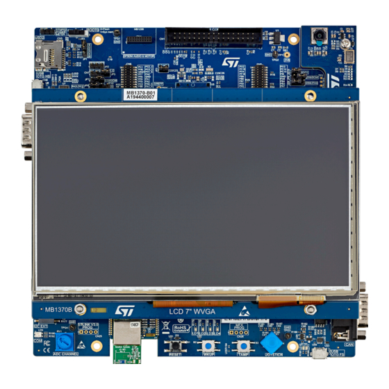
Figure 1.
STM32H7B3I-EVAL Evaluation board (top view)
Picture is not contractual.
UM2662 - Rev 1 - February 2020
www.st.com
For further information contact your local STMicroelectronics sales office.
Advertisement
Table of Contents

Related Manuals for ST STM32H7B3I-EVAL


Summary of Contents for ST STM32H7B3I-EVAL
-
Page 1: Figure 1. Stm32H7B3I-Eval Evaluation Board (Top View)
STLINK-V3E debugger/programmer. The full range of the STM32H7B3I-EVAL hardware features helps to develop applications and evaluate all the peripherals, such as USB OTG_HS and FS, CAN FD, USART, ADC and DAC, digital microphones, SRAM, SDRAM, NOR Flash memory, Octo- ™... -
Page 2: Features
DFSDM microphones daughterboard expansion connector – Motor-control interface expansion connector – C expansion connector • Flexible power-supply options: ST-LINK, USB V or external sources • On-board STLINK-V3E debugger/programmer with USB re-enumeration capability: mass storage, Virtual COM port, and debug port •... -
Page 3: Ordering Information
Evaluation tools marked as “ES” or “E” are not yet qualified and therefore not ready to be used as reference design or in production. Any consequences deriving from such usage will not be at ST charge. In no event, ST will be liable for any customer usage of these engineering sample tools as reference designs or in production. -
Page 4: Development Environment
STM32 Flash memory for easy demonstration of the device peripherals in standalone mode. The latest versions of the demonstration source code and associated documentation can be downloaded from www.st.com. UM2662 - Rev 1 page 4/95... -
Page 5: Conventions
UM2662 Conventions Conventions Table 3 provides the conventions used for the ON and OFF settings in the present document. Table 3. ON/OFF convention Convention Definition Jumper JPx ON Jumper fitted Jumper JPx OFF Jumper not fitted Jumper JPx [1-2] Jumper should be fitted between Pin 1 and Pin 2 Solder bridge SBx ON SBx connections closed by 0 Ω... -
Page 6: Delivery Recommendations
UM2662 Delivery recommendations Delivery recommendations Some verifications are needed before using the board for the first time to make sure that nothing was damaged during shipment and that no components are unplugged or lost. When the board is extracted from its plastic bag, ™... -
Page 7: Hardware Layout And Configuration
UM2662 Hardware layout and configuration Hardware layout and configuration The STM32H7B3I-EVAL Evaluation board is designed around the STM32H7B3LIH6QU target microcontroller. Figure 2 illustrates STM32H7B3LIH6QU connections with peripheral components. Figure 2. Hardware block diagram 3V3 Power Supply (3V3_AO) STM32H7B3LIH6QU GPIOs LED, push-button, and wake-up... -
Page 8: Figure 3. Stm32H7B3I-Eval Evaluation Board Layout
Hardware layout and configuration Figure 3 shows the location of the main components on the top side of the Evaluation board. Figure 3. STM32H7B3I-EVAL Evaluation board layout CN4: MB1299 DFSDM microphones module connector CN1: Motor-control connector SW1: BOOT0 switch JPME1: Power meter connector CN3: microSD™... -
Page 9: Embedded Stlink-V3E
• Using an external debug tool Embedded STLINK-V3E 6.1.1 Description The STLINK-V3E programming and debugging tool is integrated into the STM32H7B3I-EVAL Evaluation board. The embedded STLINK-V3E supports: • 5 V power supplied by the CN21 USB connector • USB 2.0 high-speed-compatible interface •... -
Page 10: Drivers
UM2662 Embedded STLINK-V3E 6.1.3 Drivers Before connecting the STM32H7B3I-EVAL board to a Windows PC via USB, the user must install a driver for the STLINK-V3E (not required for Windows 10). It is available on the www.st.com website. In case the STM32H7B3I-EVAL board is connected to the PC before the driver is installed, some STM32H7B3I- EVAL interfaces may be declared as “Unknown”... -
Page 11: External Jtag, Swd, And Trace
UM2662 External JTAG, SWD, and trace External JTAG, SWD, and trace 6.2.1 Description There are two basics ways to support an external debug tool. If the user encounters any trouble with the first procedure, then the second one is mandatory. Keep the embedded STLINK-V3E running. -
Page 12: Limitations And Hardware Configuration - Etm Trace (Cn15)
UM2662 External JTAG, SWD, and trace 6.2.2 Limitations and hardware configuration - ETM trace (CN15) ® Limitations: Wi‑Fi , LCD, SAI, FMC A19-22 cannot be used at the same time as TRACE. If the best performance of ETM is required (84 MHz/98 MHz), refer to Table 4. -
Page 13: Limitations And Hardware Configuration - Jtag (Cn14) Or Mipi10 (Cn16)
UM2662 External JTAG, SWD, and trace 6.2.3 Limitations and hardware configuration - JTAG (CN14) or MIPI10 (CN16) Limitations: STM32H7B3LIH6QU JTAG cannot be connected at the same time to STLINK-V3E and to CN14 or CN16 connector. To be able to use JTAG on CN14 or CN16 connector, it is necessary to disconnect JTAG signals from STLINK-V3E (JTMS, JTCK, JTDO, and NRST). -
Page 14: Table 7. Etm Trace Debugging Connector Cn15
UM2662 External JTAG, SWD, and trace MIPI10 STDC14 CN16 Designation T_VCP_RX Target RX used for VCP (must be UART dedicated to Bootloader) T_VCP_TX Target TX used for VCP (must be UART dedicated to Bootloader) Figure 7. ETM trace debugging connector CN15 Table 7. -
Page 15: Table 8. Jtag / Swd Debugging Connector Cn14
UM2662 External JTAG, SWD, and trace Figure 8. JTAG debugging connector CN14 Table 8. JTAG / SWD debugging connector CN14 Pin number Description Pin number Description +3.3V +3.3V TRST(PB4) TDI(PA15) TMS/SWDIO(PA13) TCK/SWCLK(PA14) RTCK TDO/SWO(PB3) RESET# DBGRQ(PJ7) DBGACK(PJ12) UM2662 - Rev 1 page 15/95... -
Page 16: Power Supply
The STM32H7B3I-EVAL Evaluation board can be powered from ST-LINK USB connector CN21 (“STLK”), but only the ST-LINK circuit has the power before USB enumeration, for the host PC only provides 100 mA to the boards at that time. During the USB enumeration, the STM32H7B3I-EVAL board asks for the 500 mA power to the Host •... -
Page 17: Board Power Supply - Hardware Configuration
STM32H7B3I-EVAL, JP29 is set as shown on the right. For power supply jack(CN17) to the STM32H7B3I-EVAL, JP29 is set as shown on the right. For power supply from USB OTG HS (CN14) to STM32H7B3I-EVAL, JP29 is set as shown on the right. JP29 For power supply from USB OTG FS (CN27) to STM32H7B3I-EVAL, JP29 is set as shown on the right. -
Page 18: Figure 9. Power Supply Connector Cn17
Configure USB HS PHY into Low Power Mode (Register Address=04, bit 6 in USB PHY). The STM32H7B3I-EVAL Evaluation board can be powered from a DC 5V power supply via the external power supply jack (CN17) shown in Figure 9. -
Page 19: Board Power Supply - Smps / Ldo Configuration
Power supply 6.3.3 Board power supply - SMPS / LDO configuration Figure 10. MCU Power : SMPS / LDO STM32H7B3I-EVAL supports four “SMPS / LDO” configurations of the STM32H7B3LIH6QU microcontroller described in Table LDO supply only SMPS supply only (Default configuration) -
Page 20: Figure 11. Config1 - Ldo Only
UM2662 Power supply Figure 11. Config1 - LDO only Figure 12. Config2 - SMPS only (Default configuration) UM2662 - Rev 1 page 20/95... -
Page 21: Figure 13. Config3 - Smps And Ldo Cascaded
A deadlock occurs if the board SMPS/LDO firmware PWR configuration does not match its hardware configuration: after the reset, the ST-LINK cannot connect the target anymore. The firmware PWR configuration must be set as follows in function SystemClock_Config in file main.c: •... -
Page 22: Board Power Supply - Vdd50_Usb And Vregoutv33V
UM2662 Power supply If a deadlock occurs because of a mismatch between hardware and firmware PWR settings (SMPS/LDO), the user can recover the board by applying the following procedure: Power off the board. Set SW1 (BOOT0) to 1 (system memory). This changes the BOOT0 pin to 1 instead of 0, thus changing the device boot address to boot address 1 and making the bootloader start in System memory. -
Page 23: Board Power Supply - Vddmmc
UM2662 Power supply 6.3.5 Board power supply - VDDMMC STM32H7B3I-EVAL can provide either 1.8 V or 3.3 V on VDDMMC power rail of the STM32H7B3LIH6QU microcontroller. Figure 17. MCU Power: VDDMMC This power rail can be used in different configurations: •... -
Page 24: Table 13. Vddmmc Default Hardware Configuration For '3.3V Only' Functions
UM2662 Power supply Remember: The user must force VDDMMC at 3.3 V when using any of these functions: • OCSPI1: Refer to Section 7.7 • LED1: Refer to Section 7.10 • Camera: Refer to Section 7.11 • MEMS LED and DFSDM: Refer to Section 7.2 •... -
Page 25: Table 15. Vddmmc Hardware Configuration For '1.8V / 3.3V' Function (Sdio2)
UM2662 Power supply For SD card 2 (SDIO2) interface, in order to control independently 1V8_SW, 3V3_SW, and VDDMMC, it is necessary to control following GPIOs with software: • SD_LDO_SEL (PG6) • 3V3_SW_ENABLE (MFX IO0) • 1V8_SW_ENABLE (MFX IO8) And the user must follow the hardware configuration described in Table Table 15. -
Page 26: Figure 19. 3V3_Sw And 1V8_Sw Ldos Schematic
UM2662 Power supply Figure 19. 3V3_SW and 1V8_SW LDOs schematic (page 20) Figure 20. VDDIO_MMC switch schematic (Page 21) UM2662 - Rev 1 page 26/95... -
Page 27: Clock, Reset, And Boot
Clock, reset, and boot 6.4.1 Clock source Two clock sources are available on the STM32H7B3I-EVAL Evaluation board for STM32H7B3LIH6QU and its embedded RTC, and other clock sources for their peripherals. • 24 MHz crystal X1 for the STM32H7B3LIH6QU microcontroller. It can be disconnected by removing R20 and R21 when the internal RC clock is used. -
Page 28: Reset Source
UM2662 VCP ST-LINK UART 6.4.2 Reset source The reset signal of STM32H7B3I-EVAL Evaluation board is active low and the reset sources include: • Reset button B1 • Debugging tools from JTAG/SWD connector CN14 and ETM trace connector CN15 • Daughterboard from CN6 •... -
Page 29: Hardware Configuration
RS-232 communication is supported by D-type 9-pins RS-232 connector CN9, which is connected to PB14/PB15 (Default configuration) or PA2/PA3 (Compatible with bootloader) pins of STM32H7B3LIH6QU on the STM32H7B3I-EVAL Evaluation board through ST3241EBPR RS-232 transceiver U9. The Bootloader_RESET and Bootloader_BOOT0 signals are added on RS-232 connector CN9 for ISP support. -
Page 30: Interface
UM2662 RS-232 UART RS-232 UART on PA2/PA3 Important: Audio I2S6, USB HS, and motor control cannot be used with VCP UART PA2/PA3. Hardware modifications are listed in Table Table 23. RS-232 UART related jumpers (PA2/PA3: Bootloader) Pin name Setting STLINK-V3E VCP (Bootloader) JP21 / SB42 PA2 (MCU TX) JP39 / SB50... -
Page 31: Primary Functions
UM2662 Primary functions Primary functions The functions described in the chapter below do not have any usage limitations with each other, except Camera and Audio. For further details, refer to Section 7 Primary functions. Audio 7.1.1 Description An audio codec CS42L51-CNZ is connected to either I2S6 or SAI interface of STM32H7B3LIH6QU (Refer to Table 25 below for configurations) to support the TDM feature. -
Page 32: Interface
C address of CS42L51-CNZ is 0x94 (AD0=0). 7.1.4 Interface A 3.5 mm stereo audio jack CN20 is available on STM32H7B3I-EVAL Evaluation board to support headset (Headphone and microphone integrated). A 3.5 mm stereo audio jack CN18 is available on STM32H7B3I-EVAL Evaluation board to support external speaker. -
Page 33: Dfsdm Microphones Module (Mb1299)
UM2662 DFSDM microphones module (MB1299) DFSDM microphones module (MB1299) 7.2.1 Description A DFSDM Beam Forming microphone module (MB1299) can be connected to STM32H7B3LIH6QU DFSDM interface through CN4. MB1299 module embeds five DFSDM MEMS microphones STMicroelectronics MP34DT01TR-M: • One microphone for detection in the center (CLK_0, DATA_0) •... -
Page 34: Operating Voltage
UM2662 DFSDM microphones module (MB1299) 7.2.2 Operating voltage DFSDM microphone module supports only 3.3 V. Make sure to supply 3.3 V on VDDMMC (Refer to Section 6.3.5 7.2.3 Limitations and hardware configuration Limitations with primary functions: camera (Refer to jumper configuration in Table Limitations with secondary functions: USB HS and NOR Flash Hardware modifications are listed in... -
Page 35: Usb Otg Fs
500 mA). VBUS Note: The STM32H7B3I-EVAL board must be powered by an external power supply when using the OTG function. 7.3.2 Operating voltage The STM32H7B3LIH6QU USB OTG FS interface can only be at 3.3 V on this board. -
Page 36: Limitations And Hardware Configuration
EXT I C connector 7.5.1 Description I2C2 bus of STM32H7B3LIH6QU is connected to CN24 on STM32H7B3I-EVAL. The I C functional daughterboard can be mounted on CN24 and accessed by the microcontroller via the I2C2 bus. EXT_RESET is controlled by MFX_GPO6 signal. -
Page 37: Interface
UM2662 32-bit SDRAM 7.5.3 Limitations and hardware configuration ® I2C2 (PH4/PH5) is shared between EXT I C module CN24, MB1486 Wi‑Fi module U24, MFX I/O expander U25, audio codec U48, MB1379 camera module CN2, and MB1370 LCD touch panel CN30. 7.5.4 Interface Figure 26. -
Page 38: Octo-Spi Nor Flash 1
7.7.1 Description One 512-Mbit Octo-SPI NOR Flash Macronix MX25LM51245GXDI00 is connected to OCSPI1 interface of STM32H7B3LIH6QU on the STM32H7B3I-EVAL Evaluation board. 7.7.2 Operating voltage STM32H7B3LIH6QU OCSPI1 interface can only be at 3.3 V on this board. Make sure to supply 3.3 V on VDDMMC (Refer to Section 6.3.5... -
Page 39: Analog Input
UM2662 Analog input Hardware modifications are listed in Table Table 33. OCSPI1 hardware configuration Signal name Pin name Setting OCSPI1 OCSPI1_IO6 / SDIO2_CK [1-2] OCSPI1_NCS / SD_LDO_SEL JP23 [1-2] 3V3_SW_ENABLE MFX IO0 SB34 1. The default setting is in bold. 2. -
Page 40: Lcd Display Module (Mb1370)
UM2662 LCD display module (MB1370) LCD display module (MB1370) 7.9.1 Description The LCD module MB1370 features a 7-inch 800x480 WVGA TFT color LCD. The ROCKTEK RK070ER9427-CT LCD is connected to STM32H7B3LIH6QU RGB (3x8 bits) interface. The FOCALTECH FT5336GQQ capacitive touch panel is connected to the STM32H7B3LIH6QU I C interface. -
Page 41: Table 35. Lcd Module Connector Cn23
UM2662 LCD display module (MB1370) Table 35. LCD module connector CN23 Pin number Description Pin connection LCD CLK PI14 LCD R0 PI15 LCD R1 LCD R2 LCD R3 LCD R4 LCD R5 LCD R6 LCD R7 LCD G0 LCD G1 LCD G2 LCD G3 PJ10... -
Page 42: Leds And Buttons
UM2662 LEDs and buttons Pin number Description Pin connection Table 36. CTP and LCD power connector CN30 Description Pin connection Description Pin connection number number 3V3_AO 3.3V CTP I2C2 SDA CTP I2C2 SCL CTP RST PC4 (not used) CTP INT Table 37. -
Page 43: Operating Voltage
UM2662 Camera module MB1379 The Wakeup B2 and Tamper/key B3 buttons3 are available as input devices. Table 40. B2 and B3 buttons Pin name Button name B2 (KEY_WKUP0) PC13 B3 (KEY_TAMP_1/WKUP2) 7.10.2 Operating voltage STM32H7B3LIH6QU LEDs and buttons interface can only be at 3.3 V on this board. For LED1, make sure to supply 3.3 V on VDDMMC (Refer to Section 6.3.5 7.11... -
Page 44: Table 41. Hardware Modifications For Camera
UM2662 Camera module MB1379 Hardware modifications are listed in Table Table 41. Hardware modifications for camera Pin name Signal name Setting Camera INT_USB_OTG_HS_OVRCR R108 DCMI_HSYNC (I2S6_WS cannot be used) [2-3] DCMI_D0 JP32 [1-2] FMC_NOR_NE1 JP35 DFSDM1_DATIN3 (Remove MB1299) JP35 / R120 OFF / OFF DCMI_D1 R113... -
Page 45: Interface
UM2662 Wi-Fi® module MB1486 7.11.4 Interface Figure 29. Camera module connector CN2 Table 42. Camera module MB1379 connector CN2 Pin number Description Pin connection Pin number Description Pin connection PH15 I2C SCL I2C SDA PLUG MFX IO4 RSTI MFX IO5 XSDN MFX IO6 PG10... -
Page 46: Table 43. Hardware Modifications For Wi-Fi
UM2662 Wi-Fi® module MB1486 7.12.3 Limitations and hardware configuration Limitations with secondary functions: FMC A19, A21-23, trace, and SAI. ® I2C2 (PH4/PH5) is shared between EXT I C module CN24, MB1486 Wi‑Fi module U24, MFX I/O expander U25, audio codec U48, MB1379 camera module CN2, and MB1370 LCD touch panel CN30. Hardware modifications are listed in Table 43 below:... -
Page 47: Table 44. Wi-Fi ® Module Interposer Connector U24
UM2662 Wi-Fi® module MB1486 7.12.4 Interface ® Figure 30. Wi‑Fi module interposer footprint (Top view) ® Table 44. Wi‑Fi module interposer connector U24 Description Pin connection Description Pin connection number number VDD_5V I2C SDA I2C SCL WIFI DATA RDY MFX IO2 WIFI BOOT MFX IO14 SPI MOSI... -
Page 48: Mfx (Multi-Function Expander)
7.13 MFX (Multi-function expander) 7.13.1 Description The MFX circuit on the STM32H7B3I-EVAL Evaluation board acts as an I/O expander. The communication interface between MFX and STM32H7B3LIH6QU is the I2C2 bus. ® I2C2 (PH4/PH5) is shared between EXT I C module CN24, MB1486 Wi‑Fi module U24, MFX I/O expander U25, audio codec U48, MB1379 camera module CN2, and MB1370 LCD touch panel CN30. -
Page 49: Interface
UM2662 MFX (Multi-function expander) 7.13.3 Limitations and hardware configuration Limitations with a secondary function: When using motor control CN1, EXT_I2C CN24 cannot be used as MFX_GPO6 is used for both. 7.13.4 Interface The connector CN26 is used only for MFX (Multi-Function eXpander) programming during board manufacturing. It is not populated by default and not for the end-user. -
Page 50: Secondary Functions
UM2662 Secondary functions Secondary functions Functions described in the chapter below have usage limitations with primary functions or with each other. For further details, Refer to Section 8 Secondary functions for further details. SRAM 8.1.1 Description 1Mx16bit SRAM ISSI IS61WV102416BLL-10MLI is connected to bank1 NOR/PSRAM2 of FMC interface and both 8-bit and 16-bit access are allowed by BLN0 and BLN1 connected to BLE and BHE of SRAM respectively. -
Page 51: Limitations And Hardware Configuration For Sram A19 (Just For The Test)
UM2662 SRAM Hardware modifications are listed in Table 46 below: Table 46. Configuration for SRAM A0-A5, A10-11 addresses, and command Pin name Signal name Setting SRAM FMC_A0 R339 OCSPI2_IO0 FMC_A1 R335 OCSPI2_IO1 FMC_A2 R331 OCSPI2_IO2 FMC_A3 OCSPI2_IO3 FMC_A10 OCSPI2_IO4 FMC_A11 R333 OCSPI2_IO5 FMC_A4... -
Page 52: Nor
UM2662 Hardware modifications are listed in Table 47 below: Table 47. Configuration for SRAM A19 (Just for the test) Pin name Signal name Setting SRAM SAI1_SD_B JP34 WIFI_SPI4_NSS R337 TRACED0 FMC_A19 ON just for test 1. Remove to avoid stub if necessary. Note: If using SD card 1 (Default configuration), use FMC_NE3 = PG10, then SD card 2 cannot be used). -
Page 53: Limitations And Hardware Configuration For Nor A19-A22 (Just For The Test)
UM2662 Hardware modifications are listed in Table 48 below. Table 48. Configuration for NOR A0-A5, A10-11 addresses, and command Pin name Signal name Setting FMC_A0 R339 OCSPI2_IO0 FMC_A1 R335 OCSPI2_IO1 FMC_A2 R331 OCSPI2_IO2 FMC_A3 OCSPI2_IO3 FMC_A10 OCSPI2_IO4 FMC_A11 R333 OCSPI2_IO5 FMC_A4 OCSPI2_CLK R319... -
Page 54: Microsd™ Card 2
UM2662 microSD™ card 2 Hardware modifications are listed in Table 49 below: Table 49. Configuration for SRAM A19-A22 (Just for the test) Pin name Signal name Setting SAI1_SD_B JP34 WIFI_SPI4_NSS R337 TRACED0 FMC_A19 ON just for test SAI1_FS_A JP26 TRACED1 R340 DCMI_D4 R116... -
Page 55: Interface
UM2662 microSD™ card 2 Hardware modifications are listed in Table 50 below: Table 50. Configuration for NOR A0-A5, A10-11 addresses, and command Signal name Setting SDIO2 configuration SDIO2_D0 (PG9) (DCMI_VSYNC) JP17 [2-3] R118 R115 SDIO2_D1 (PG10) R280 [2-3] R257 SDIO2_D2 (PG11) (DCMI_D3) [2-3] SDIO2_D3 (PG12) R122... -
Page 56: Usb Otg Hs
SB31 and fitting SB13. USB high-speed PHY (U7) REFCLK pin is connected to an external 24 MHz oscillator (X3). The STM32H7B3I-EVAL Evaluation board can be powered by this USB connector (CN8) at 5V DC with 500mA current limitation. -
Page 57: Interface
UM2662 DFSDM STMP2 and PT100 monitoring Hardware modifications are listed in Table Table 52. USB OTG HS function configuration Signal name Pin name Setting USB HS (CN8) ULPI_D0 / I2S6_MCK [2-3] ULPI_D1 / DFSDM12_CKOUT JP10 ULPI_D5 / DFSDM12_DATIN1 PB12 JP19 [2-3] ULPI_D7 JP16... -
Page 58: Ocspi Nor Flash 2 Module (Mb1242)
Table 55. These connectors are connected to OCSPI2 interface of STM32H7B3LIH6QU on the STM32H7B3I-EVAL Evaluation board. WARNING: Due to board design, as OCSPI2 interface is “shared” with SDRAM and camera, it can only be tested at low speed (Maximum: 50 MHz). -
Page 59: Table 56. Ocspi2 Hardware Configuration
UM2662 OCSPI NOR Flash 2 module (MB1242) Hardware modifications are listed in Table 56 below: Table 56. OCSPI2 hardware configuration Signal name Pin name Setting OCSPI2 FMC_A0 R339 OCSPI2_IO0 FMC_A1 R335 OCSPI2_IO1 FMC_A2 R331 OCSPI2_IO2 FMC_A3 OCSPI2_IO3 FMC_A10 OCSPI2_IO4 FMC_A11 R333 OCSPI2_IO5 FMC_A4... -
Page 60: Interface
UM2662 OCSPI NOR Flash 2 module (MB1242) 8.6.4 Interface Figure 32. MB1242 OCSPI module connectors CN10 and CN11 Find CN10 (Left) pin-out in Table Table 57. CN10 (Left) MB1242 pin-out Description Pin connection Description Pin connection number number OCSPI2_NCS PG12 3V3_AO 3V3_AO OCSPI2_IO0... -
Page 61: Can Fd
8.7.1 Description The STM32H7B3I-EVAL Evaluation board supports one channel of flexible data rate CAN, CAN‑FD compliant bus communication based on 3.3 V CAN transceiver. To use CAN FD, fit SB36 and SB35 solder bridges (And remove these solder bridges when using USB OTG FS, to avoid stubs). -
Page 62: Motor Control
UM2662 Motor control Table 59. CN10 (Left) MB1242 pin-out Pin number Description Pin number Description 1,4,8,9 CANH CANL 3,5,6 Motor control 8.8.1 Description Motor-control functions can be accessed: • Either through the 17x2 legacy connector CN1, • or through the 10x2 DFSDM connector CN4. 8.8.2 Operating voltage The STM32H7B3LIH6QU motor-control interfaces (Such as GPIO, PWM, and ADC) can only be at 3.3 V on this... -
Page 63: Table 61. Motor-Control Dfsdm Connector Cn4 (10X2)
UM2662 Motor control Pin name Fitted Not fitted MCU function Motor-control function R363 R364 INT_JOY_LEFT JOYSTICK LEFT R386 R128 INT_JOY_RIGHT JOYSTICK RIGHT R360 R351 INT_JOY_SEL JOYSTICK SEL PH13 R389 R131 INT_JOY_UP JOYSTICK UP R301 R308 TIM1_CH1 PWM_1H TIM1_CH1N PWM_1L R294 TIM1_CH2 PWM_2H PB14... - Page 64 UM2662 Motor control Pin name Fitted MCU function Motor-control function fitted R282 R286 DFSDM_1_DATIN2 MOTOR_DFSDM_1_DATIN2 DFSDM1_CKIN1_DFSDM2_CKI MOTOR_DFSDM1_CKIN1_DFS PB13 R314 R316 DM2_CKIN1 R123 R384 DFSDM1_CKIN3 MOTOR_DFSDM1_CKIN3 R284 R285 DFSDM1_CKIN4 MOTOR_DFSDM1_CKIN4 R238 DFSDM1_CKIN5 MOTOR_DFSDM1_CKIN5 DFSDM1_CKIN7 MOTOR_DFSDM1_CKIN7 PB12 JP19 [1-2] DFSDM1_DATIN1 MOTOR_DFSDM1_DATIN1 JP35 [2-3] DFSDM1_DATIN3 MOTOR_DFSDM1_DATIN3 PE10...
-
Page 65: Fmc Memory Extension Connectors Cn12 And Cn13
Table Table 64, and Table Table 62. Memory connector CN12 left odd pins How to disconnect with function Pin number Pin name STM32H7B3I-EVAL pin name block on STM32H7B3I- EVAL board FMC_SDR_SDNE1 PF13 FMC_A7 R325 PF12 FMC_A6 || MOTOR_ADC1_INP6 R326 FMC_A11 || OCSPI2_IO5... -
Page 66: Table 63. Memory Connector Cn12 Left Even Pins
FMC memory extension connectors CN12 and CN13 Table 63. Memory connector CN12 left even pins How to disconnect with function Pin number Pin name STM32H7B3I-EVAL pin name block on STM32H7B3I- EVAL board FMC_SDR_SDNWE || MOTOR_ADC12_INP7 R322 PF14 FMC_A8 FMC_A10 || OCSPI2_IO4... -
Page 67: Table 64. Memory Connector Cn13 Right Odd Pins
Table 64. Memory connector CN13 right odd pins How to disconnect with function Pin number Pin name STM32H7B3I-EVAL pin name block on STM32H7B3I- EVAL board FMC_A5 || OCSPI2_NCLK FMC_A4 || OCSPI2_CLK FMC_A3 || OCSPI2_IO3 WIFI_SPI4_MOSI || SAI1_SD_A || FMC_A22 || TRACED3 ||... -
Page 68: Table 65. Memory Connector Cn13 Right Even Pins
FMC memory extension connectors CN12 and CN13 Table 65. Memory connector CN13 right even pins How to disconnect with function Pin number Pin name STM32H7B3I-EVAL pin name block on STM32H7B3I- EVAL board FMC_SDR_SDCKE1 R320 WIFI_SPI4_MISO || SAI1_SCK_A || FMC_A21 || TRACED2 || MOTOR_TIM15_CH1... -
Page 69: Daughterboard Extension Connectors Cn5 And Cn6
Daughterboard extension connectors CN5 and CN6 Two 60-pin male headers CN5 and CN6 can be used to connect with a daughterboard or a standard wrapping board to the STM32H7B3I-EVAL Evaluation board. All GPIOs are available on them and memory connectors (CN12 and CN13). -
Page 70: Table 67. Daughterboard Extension Connector Cn6 Left Even Pins
UM2662 Daughterboard extension connectors CN5 and CN6 Table 67. Daughterboard extension connector CN6 left even pins Pin number Pin name Pin function How to disconnect PC2_C FREE ADC PC3_C MOTOR_ADC2_INP1 R219 OSC_OUT R20 / SB6 KEY_WKUP0 || MOTOR_TIM2_CH1 R229 LCD_BL_CTRL || MOTOR_TIM2_CH2 R236 LCD_RESET || MOTOR_TIM2_CH3 || BOOTLOADER_VCP_TX JP40... -
Page 71: Table 68. Daughterboard Extension Connector Cn5 Right Odd Pins
UM2662 Daughterboard extension connectors CN5 and CN6 Table 68. Daughterboard extension connector CN5 right odd pins Pin number Pin name Pin function How to disconnect PI12 RGB_LCD_HSYNC R215 PC15 OSC32_OUT PI14 RGB_LCD_CLK R226 PF10 INT_uSDCard_Detect1 DCMI_D7 || DFSDM1_DATIN7 R104 DCMI_D6 || MEMS_LED || MOTOR_DFSDM1_CKIN7 R110 INT_USB_OTG_FS_OVRCR || MOTOR_DFSDM1_CKIN5 RGB_LCD_B7... -
Page 72: Table 69. Daughterboard Extension Connector Cn5 Right Even Pins
UM2662 Daughterboard extension connectors CN5 and CN6 Table 69. Daughterboard extension connector CN5 right even pins Pin number Pin name Pin function How to disconnect PI13 RGB_LCD_VSYNC R214 PC14 OSC32_IN KEY_TAMP_1/WKUP2 PC13 INT_MFX_IRQ_OUT R168 DCMI_PIXCLK || I2S6_EXT_SD_BKUP || MOTOR_TIM1_BKIN I2S6_EXT_SD || NJTRST JTDO/TRACESWO RGB_LCD_DE R248... -
Page 73: Appendix Astm32H7B3I-Eval I/O Assignment
UM2662 STM32H7B3I-EVAL I/O Assignment Appendix A STM32H7B3I-EVAL I/O Assignment Table 70. STM32H7B3I-EVAL I/O Assignment Main function pinout Optional function pinout LQFP144 pinout Pin name Motor-control connector assignment assignment TRACE_CLK SRAM-FMC_A19 SRAM-FMC_A20 TRACE_D2 LCD_RS_FMC_A22 TRACE_D3 VBAT POWER PC13 User Button WKUP2... - Page 74 UM2662 STM32H7B3I-EVAL I/O Assignment Main function pinout Optional function pinout LQFP144 pinout Pin name Motor-control connector assignment assignment ADC12_IN7 OCTOSPI_NCS TIM2_CH3 OCTOSPI_CLK OPAMP1_VOUT ADC12_IN8 POWER POWER ADC12_IN9/DAC1_OUT1 UCPD_ADC12_IN9 STMOD+_SPI3_NSS ADC12_IN9 PMOD_SPI3_NSS LCD_BL_CTRL TIM2_CH1 STMOD+_TIM2_CH1 OCTOSPI_IO3 ADC12_IN11 OCTOSPI_IO2 TIM8_CH1N OCTOSPI_IO1 TIM8_CH2N...
- Page 75 UM2662 STM32H7B3I-EVAL I/O Assignment Main function pinout Optional function pinout LQFP144 pinout Pin name Motor-control connector assignment assignment VDD_SMPS POWER POWER VSS_SMPS POWER POWER POWER POWER STMOD+_LPUART1_CTS PB13 RS-232 LPUART1_CTS PMOD_LPUART1_CTS PB14 UCPD_DB2 PB15 UCPD_CC2 LCD-SRAM-FMC_D13 LCD-SRAM-FMC_D14 PD10 LCD-SRAM-FMC_D15 PD11...
- Page 76 UM2662 STM32H7B3I-EVAL I/O Assignment Main function pinout Optional function pinout LQFP144 pinout Pin name Motor-control connector assignment assignment PA10 Audio SAI1_SD_A PA11 USB_DM PA12 USB_DP PA13 SWDIO JTAG_JTMS VDDUSB POWER POWER POWER PA14 SWCLK JTAG_JTCK PA15 UCPD_CC JTAG_JTDI PC10 SDIO_D2...
- Page 77 UM2662 STM32H7B3I-EVAL I/O Assignment Main function pinout Optional function pinout LQFP144 pinout Pin name Motor-control connector assignment assignment Touch key BOOT0 FDCAN1_RX FDCAN1_TX SRAM_FMC_NBL0 SRAM_FMC_NBL1 POWER POWER POWER UM2662 - Rev 1 page 77/95...
-
Page 78: Appendix Bmfx I/O Assignment
UM2662 MFX I/O Assignment Appendix B MFX I/O Assignment Table 71. MFX I/O Assignment Signal name Pin name WIFI_SPI4_SCK MFX IO0 MFX_3V3_SW_ENABLE MFX IO1 MFX_WIFI_GPIO MFX IO2 MFX_WIFI_DATRDY MFX IO3 MFX_Audio_RST MFX IO4 MFX_Camera_PLUG_IN MFX IO5 MFX_Camera_RSTI MFX IO6 MFX_Camera_XSDN MFX IO7 MFX_USB_OTG_FS_PWR_EN MFX IO8... -
Page 79: Appendix Cstm32H7B3I-Eval Mechanical Drawing
UM2662 STM32H7B3I-EVAL mechanical drawing Appendix C STM32H7B3I-EVAL mechanical drawing MB1331 with 7’’ LCD daughterboard (RGB) Figure 36. Mechanical dimensions (in millimeters) Table 72. Mechanical dimensions (In millimeters) Symbol Size Symbol Size Symbol Size 68.6 116.5 32.7 48.6 21.4 1.27 33.5 60.7... -
Page 80: Appendix D Primary Functions Supported By Default
UM2662 Primary functions supported by default Appendix D Primary functions supported by default Two main use case combinations are supported by default on the board with no limitations between these “primary” functions, and no hardware rework needed: Use case 1 (Audio) Following functions can be used at the same time without any limitations from each other: •... -
Page 81: Figure 37. Primary Features - Use Case Compatibility Matrix
UM2662 Primary functions supported by default Figure 37. Primary features - Use case compatibility matrix UM2662 - Rev 1 page 81/95... -
Page 82: Appendix E Secondary Functions Supported With Limitations
UM2662 Secondary functions supported with limitations Appendix E Secondary functions supported with limitations Following secondary functions have limitations and cannot be used together with at least one of the primary functions supported by default on the board: • • SRAM •... -
Page 83: Appendix F Federal Communications Commission (Fcc) And Industry Canada (Ic)
Federal Communications Commission (FCC) and Industry Canada (IC) Compliance Statements Appendix F Federal Communications Commission (FCC) and Industry Canada (IC) Compliance Statements Applicable for STM32H7B3I-EVAL Evaluation kit products with order code STM32H7B3I-EVAL (containing ISM43340-M4G-L44-10CF module). FCC Compliance Statement Contains FCC ID: O7P-341 Part 15.19... -
Page 84: Ce Conformity
Avertissement : cet équipement est conforme à la Classe A de la EN55032 / CISPR 32. Dans un environnement résidentiel, cet équipement peut créer des interférences radio. F.3.2 Simplified declaration of conformity Hereby, STMicroelectronics declares that the radio equipment types STM32H7B3I-EVAL is in compliance with Directive 2014/53/EU. UM2662 - Rev 1 page 84/95... -
Page 85: Revision History
UM2662 Revision history Table 73. Document revision history Date Revision Changes 18-Feb-2020 Initial release. UM2662 - Rev 1 page 85/95... -
Page 86: Table Of Contents
UM2662 Contents Contents Features................2 Ordering information . - Page 87 VCP ST-LINK UART ........
- Page 88 UM2662 Contents EXT I C connector ............36 7.5.1 Description .
- Page 89 UM2662 Contents 7.12.2 Operating voltage ............45 7.12.3 Limitations and hardware configuration .
- Page 90 STM32H7B3I-EVAL I/O Assignment ........73...
- Page 91 UM2662 Contents Contents ................86 List of tables .
- Page 92 UM2662 List of tables List of tables Table 1. List of available products............. . . 3 Table 2.
- Page 93 STM32H7B3I-EVAL I/O Assignment ........
- Page 94 STM32H7B3I-EVAL Evaluation board (top view) ........
- Page 95 ST’s terms and conditions of sale in place at the time of order acknowledgement. Purchasers are solely responsible for the choice, selection, and use of ST products and ST assumes no liability for application assistance or the design of Purchasers’...
Need help?
Do you have a question about the STM32H7B3I-EVAL and is the answer not in the manual?
Questions and answers