Table of Contents
Advertisement
UM2324
User manual
STM32 Nucleo-64 boards with STM32G07xRB MCUs
Introduction
The STM32 Nucleo-64 boards (NUCLEO-G070RB and NUCLEO-G071RB) provide an
affordable and flexible way for users to try out new concepts and build prototypes with the
STM32 microcontroller, which provide various combinations of performance, power
consumption and features.
Arduino™ Uno V3 connectivity and ST morpho headers provide easy means of expanding
the functionality of the Nucleo open development platform with a wide choice of specialized
shields.
The STM32 Nucleo-64 boards do not require any separate probe, as it integrates the
ST-LINK/V2-1 debugger/programmer. The STM32 Nucleo-64 boards come with the
comprehensive free STM32 software libraries and examples that are available with the
STM32Cube package.
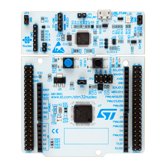
Figure 1. NUCLEO-G070RB/NUCLEO-G071RB top view
Picture is not contractual.
October 2018
UM2324 Rev 2
1/44
www.st.com
1
Advertisement
Table of Contents

Related Manuals for ST STM32 Nucleo-64


Summary of Contents for ST STM32 Nucleo-64
-
Page 1: Figure 1. Nucleo-G070Rb/Nucleo-G071Rb Top View
Nucleo open development platform with a wide choice of specialized shields. The STM32 Nucleo-64 boards do not require any separate probe, as it integrates the ST-LINK/V2-1 debugger/programmer. The STM32 Nucleo-64 boards come with the comprehensive free STM32 software libraries and examples that are available with the STM32Cube package. -
Page 2: Table Of Contents
Embedded ST-LINK/V2-1 ........12... - Page 3 Arduino Uno V3 connectors ........28 ST morpho connectors CN7 and CN10 ......31 Appendix A NUCLEO-G070RB or NUCLEO-G071RB I/O assignment .
- Page 4 ST-LINK jumper configuration ........
- Page 5 Figure 18. NUCLEO-G070RB ST morpho connector pinout ....... . 32 Figure 19.
-
Page 6: Features
Any consequences deriving from such usage will not be at ST charge. In no event, ST will be liable for any customer usage of these engineering sample tools as reference design or in production. -
Page 7: Ordering Information
UM2324 Ordering information Ordering information To order the STM32 Nucleo-64 board corresponding to the targeted STM32, refer to Table Table 1. Ordering information Order code Target STM32 NUCLEO-G070RB STM32G070RBT6 NUCLEO-G071RB STM32G071RBT6 The meaning of the NUCLEO-G071RB codification is explained in Table Table 2. -
Page 8: Quick Start
[1-2], JP3 (IDD) on. For a correct identification of all device interfaces from the host PC, install the Nucleo USB driver available on the www.st.com/stm32nucleo web page, prior to connecting the board. To power the board, connect the STM32 NUCLEO-G070RB or NUCLEO-G071RB to a PC with a USB cable 'type-A to micro-B' through the USB connector CN2. -
Page 9: Hardware Layout And Configuration
UM2324 Hardware layout and configuration Hardware layout and configuration The STM32 NUCLEO-G070RB and NUCLEO-G071RB boards are designed around the STM32 microcontrollers in a 64-pin LQFP package. Figure 2 illustrates the connections between the STM32 and its peripherals (STLINK/V2-1, pushbutton, LED, and morpho connectors). Figure 3 Figure 4 help the user to locate these features on the NUCLEO-G070RB or... -
Page 10: Figure 3. Top Layout
Hardware layout and configuration UM2324 Figure 3. Top layout Figure 4. Bottom layout 10/44 UM2324 Rev 2... -
Page 11: Nucleo-G070Rb Or Nucleo-G071Rb Board Mechanical Drawing
The NUCLEO-G070RB or NUCLEO-G071RB board is divided into two parts: ST-Link part and target MCU part. ST-Link part PCB is cuttable to reduce board size. In this case the rest target MCU part is only powered by VIN, E5V & 3.3V on morpho connectors CN7 or VIN &... -
Page 12: Embedded St-Link/V2-1
Standalone version doesn't exist (only Nucleo and future discovery support V2-1) For all general information concerning debugging and programming features common between V2 and V2-1 please refer to ST-LINK/V2 User Manual UM1075. The embedded ST-LINK/V2-1 is usable in two different ways according to the jumper states (refer to Table •... -
Page 13: Drivers
In case the STM32 Nucleo-64-P board is connected to the PC before installing the driver, the PC device manager may report some Nucleo interfaces as ‘Unknown’. To recover from this situation, after installing the dedicated driver, the association of ‘Unknown’ USB devices found on the STM32 Nucleo-64-P board to this dedicated driver, must be updated in the device manager manually. -
Page 14: Using St-Link/V2-1 To Program/Debug An External Stm32 Application
Figure 7. NUCLEO-G070RB or NUCLEO-G071RB connections image 6.4.4 Using ST-LINK/V2-1 to program/debug an external STM32 application It is very easy to use the ST-LINK/V2-1 to program the STM32 on an external application. Simply remove the 2 jumpers from CN4 as shown in Figure... -
Page 15: Power Supply And Power Selection
DC power supply. It is possible to supply the STM32 NUCLEO-G070RB or NUCLEO-G071RB board with any of the following sources: • 5V_USB_STLK from ST-LINK USB connector • VIN (7 V - 12 V) from Arduino connector or ST morpho connector • E5V from ST morpho connector • 5V_USB_CHG from ST-LINK USB •... -
Page 16: Table 7. Power Supply Capabilities
5V_ST_LINK is a DC power with limitation from ST-LINK USB connector (USB type Micro-B connector of ST-LINK/V2-1). In this case JP2 jumper must be on pins 1 and 2 to select STLK power source on silkscreen of JP2. This is the default setting. If the USB enumeration succeeds, the STLK power is enabled, by asserting the PWR_ENn signal (from STM32F103CBT6). -
Page 17: Figure 9. Stlk Power Source
VIN is the 7 V to 12 V DC power from Arduino CN6 pin 8 named VIN on Arduino connector silkscreen or from ST morpho connector CN7 pin 24. In this case JP2 jumper must be on pins 3 and 4 to select VIN power source on silkscreen of JP2. In that case the DC power comes from the power supply through the Arduino Uno V3 battery shield (compatible with Adafruit PowerBoost 500 shield). -
Page 18: Figure 10. Jp2 [3-4]: Stlk Power Source
Figure 10. JP2 [3-4]: STLK power source E5V is the DC power coming from external (5V DC power from ST morpho connector CN7 pin 6). In this case JP2 jumper must be on pins 5 and 6 to select E5V power source on silkscreen of JP2. -
Page 19: Figure 11. Jp2 [5-6]: Stlk Power Source
Figure 11. JP2 [5-6]: STLK power source 5V_USB_CHARGER is the DC power charger connected to USB ST-LINK (CN2). To select the CHG power source on silkscreen of JP2, the jumper of JP2 must be on pins 7 and 8. In this case, if the STM32 NUCLEO-G070RB or NUCLEO-G071RB board is powered by an external USB charger the debug is not available. -
Page 20: External Power Supply Output
NUCLEO-G070RB or NUCLEO-G071RB board and the connected shield must be less than 500 mA. Programming/debugging when the power supply is not from ST-LINK VIN or E5V is usable as an external power supply in case the current consumption of the STM32 NUCLEO-G070RB or NUCLEO-G071RB board and its extension boards exceed the allowed current on the USB. -
Page 21: Osc Clock Sources
Check that the green LED LD3 is turned ON Connect the PC to the USB connector CN2 If this sequence is not respected, the board may be powered by VBUS first from the ST- LINK, with the following risks: •... -
Page 22: Hse: Osc 8 Mhz Clock Supply
R33 and R34 OFF • MCO from ST-LINK: MCO output of ST-LINK is used as input clock. This frequency cannot be changed, it is fixed at 8 MHz and connected to the PF0-OSC_IN of STM32 microcontroller. The configuration must be: –... -
Page 23: Uart2 Communication
The four LEDs are located on the top side of the board. LD1 COM: LD1 is a bi-color LED. LD1 default status is red. LD1 turns to green to indicate that communication is in progress between the PC and the ST-LINK/V2-1 as follow: –... -
Page 24: Push Buttons
Table 9 describes the other available jumper settings. Table 9. Jumper configuration Jumper / Function State Comment ST-LINK/V2-1 enable for on-board ON [1-2] ON [3-4] MCU debugger T_SWCLK T_SWDIO ST-LINK/V2-1 functions enabled for OFF [1-2] OFF [3-4] external CN2 connector... -
Page 25: Configuration Of The Solder Bridges
UM2324 Hardware layout and configuration 6.14 Configuration of the solder bridges Table 10 shows the solder bridge configurations and settings. Table 10. Solder bridge configurations and settings Definition Bridge State Comment SWD interface SB7/SB9 Reserved, do not modify. (default)) /SB11/SB13 SWD interface SB6/SB8 Reserved, do not modify. - Page 26 Hardware layout and configuration UM2324 Table 10. Solder bridge configurations and settings (continued) Definition Bridge State Comment PA5 controls LD4 User LED SB22 LD4 is isolated AVDD connects to CN5 PIN8 AVDD SB21 AVDD disconnects to CN5 PIN8 1. Default jumper state is shown in bold. 26/44 UM2324 Rev 2...
-
Page 27: Connectors
• CN7 and CN10: ST morpho connectors USB Micro-B connector CN2 The USB connector CN2 is used to connect the embedded ST-LINK/V2-1 to the PC for programming and debugging the STM32 NUCLEO-G070RB or NUCLEO-G071RB board microcontroller. Figure 13. USB micro-B connector CN2 (front view) -
Page 28: Arduino Uno V3 Connectors
Connectors UM2324 Arduino Uno V3 connectors The Arduino connectors CN5, CN6, CN8 and CN9 (see Figure 14) are female connectors compatible with Arduino standard. Most shields designed for Arduino fit to the NUCLEO- G070RB or NUCLEO-G071RB board. The Arduino connectors on STM32 NUCLEO-G070RB or NUCLEO-G071RB board support the Arduino Uno V3. -
Page 29: Figure 15. Nucleo-G070Rb Arduino Connector Pinout
UM2324 Connectors The related pinout for Arduino connector is showed in Figure 15 Figure 16 and listed in Table Figure 15. NUCLEO-G070RB Arduino connector pinout Figure 16. NUCLEO-G071RB Arduino connector pinout Note: Note: Arduino Uno V3 D0 and D1 signals are connected by default on USART1 (MCU I/O PC4 and PC5). -
Page 30: Table 12. Arduino Connector Pinout
Connectors UM2324 Table 12. Arduino connector pinout Connector Signal name STM32 pin Function number name Reserved for test IOREF I/O reference NRST NRST NRST RESET 3.3 V input/output 5 V output 7 V to 12 V power input ARD_A0_IN0 ARD_A1_IN1 ARD_A2_IN4 ARD_A3_IN9 PB9 or PB11... -
Page 31: St Morpho Connectors Cn7 And Cn10
STM32 NUCLEO-G070RB or NUCLEO-G071RB board (see Figure 17). All signals and power pins, except VDD_CORE 1.2 V of the STM32, are available on the ST morpho connectors. These connectors can also be probed by an oscilloscope, logical analyzer or voltmeter. -
Page 32: Figure 18. Nucleo-G070Rb St Morpho Connector Pinout
Connectors UM2324 The related pinout and the MCU assignment for the ST morpho connectors are listed in Figure 18 Figure Figure 18. NUCLEO-G070RB ST morpho connector pinout Figure 19. NUCLEO-G071RB ST morpho connector pinout Note: Arduino Uno V3 D0 and D1 signals are connected by default on USART1 (MCU I/O PA2 and PA3). -
Page 33: Appendix A Nucleo-G070Rb Or Nucleo-G071Rb I/O Assignment
UM2324 NUCLEO-G070RB or NUCLEO-G071RB I/O assignment Appendix A NUCLEO-G070RB or NUCLEO-G071RB I/O assignment Table 13. NUCLEO-G070RB or NUCLEO-G071RB I/O assignment Pin No Pin name Signal or label Main feature / optional feature (SB) PC11 PC11 PC12 PC12 PC13 PC13 User Button/IO PC14 - OSC32_IN PC14 - OSC32_IN LSE CLK/IO... - Page 34 NUCLEO-G070RB or NUCLEO-G071RB I/O assignment UM2324 Table 13. NUCLEO-G070RB or NUCLEO-G071RB I/O assignment (continued) Pin No Pin name Signal or label Main feature / optional feature (SB) PB12 PB12 ARD_A5_IN16 PB13 PB13 PB14 PB14 ARD_D6 || TIM_15_CH1 PB15 PB15 ARD_D7 ARD_D8 ARD_D9 || TIM_3_CH2 PA10...
-
Page 35: Appendix B Electrical Schematics
UM2324 Electrical schematics Appendix B Electrical schematics This section provides the design schematics for the STM32 Nucleo-64 board features. • NUCLEO-G071RB board: – Figure 20: Top – Figure 21: STM32_microcontroller_IOs – Figure 22: STM32_microcontroller_PWR – Figure 23: Arduino extension connectors –... - Page 36 Figure 20. Top ST_LINK_V2-1 Connectors ST_LINK_V2-1.SchDoc STM32_microcontroller_IOs.SchDoc Arduino_extension_connectors.SchDoc NRST NRST NRST PA[0..15] PA[0..15] PB[0..15] PB[0..15] PC[0..15] PC[0..15] PD[0..9] PD[0..9] STLK_RX UART2_TX PF[0..2] PF[0..2] STLK_TX UART2_RX NRST NRST Power STM32_microcontroller_power HW_Mechanical_Parts Power.SchDoc STM32_microcontroller_power.SchDoc HW_Mechanical_Parts.SchDoc Title: NUCLEO-G071RB Project: Variant: G071RB Revision: Reference: MB1360 C-01 Size:...
-
Page 37: Figure 21. Stm32_Microcontroller_Ios
Figure 21. STM32_microcontroller_IOs PA[0..15] PA[0..15] STM32G071RBT6 PB[0..15] PB[0..15] UART2_TX PC[0..15] UART2_RX PC[0..15] PD[0..9] PD[0..9] PF[0..2] PF[0..2] PA10 PC10 PA10 PC10 PA11 PC11 PA11 PC11 PA12 PC12 PA12 PC12 PA13 PC13 SB20 PA13 PC13 PA14 PC14 PA14-boot0 PC14-OSC32_IN PA15 PC15 PA15 PC15-OSC32_OUT TD0341X-G01-BLU HW10... -
Page 38: Figure 22. Stm32_Microcontroller_Pwr
Figure 22. STM32_microcontroller_PWR 4.7uF 100nF VBAT STM32G071RBT6 SB26 VBAT AVDD VREF+ SB28 100nF SB31 AGND AGND STM32_microcontroller_power Title: NUCLEO-G071RB Project: Variant: G071RB Revision: C-01 Reference: MB1360 Size: Date: 11-JUNE-18 Sheet:... - Page 39 Figure 23. Arduino extension connectors PA[0..15] PA[0..15] Extension connectors AVDD PB[0..15] PB[0..15] 510R GREEN PC[0..15] PC[0..15] VIN_5V BSN20 SB21 PD[0..9] PD[0..9] Morpho connector Morpho connector SB22 AGND CN10 PF[0..2] PF[0..2] PC10 PC11 PC12 NRST NRST PA14 5V_USB_CHG PA12 PA13 NRST PA11 PA15 PC13...
- Page 40 Figure 24. Power VIN_5V LDL112PV33R LD1117S50TR 5V_USB_STLK Vout Vout Shunt Fitted Gnd Tab HW13 5V_USB_CHG 100nF Shunt Fitted 1-2 10uF 10uF HW12 100nF GREEN Power Title: NUCLEO-G071RB Project: Variant: G071RB Revision: C-01 Reference: MB1360 Size: Date: 11-JUNE-18 Sheet:...
-
Page 41: St_Link_V2-1
T_SWO OSCOUT PA10 STM_RST LED_STLK NRST 100R SB17 Jumpers ON --> NUCLEO Selected VSSA PWR_ENn 3V3_STLK VDDA PB15 Jumpers OFF --> ST-LINK Selected AIN_1 T_JTMS PB14 100nF T_JTCK PB13 PB12 100R BAT60JFILM T_SWDIO_IN 5V_USB_CHG BAT60JFILM Wired on Solder Side SB16... - Page 42 Figure 26. HW Mechanical Parts HW Mechanical parts MB1360B MB1360B01 XXXX NUCLEO-G071RB BOARD REF BOARD CPN HW Mechanical parts Title: NUCLEO-G071RB Project: Variant: G071RB Revision: C-01 Reference: MB1360 Size: Date: 11-JUNE-18 Sheet:...
-
Page 43: Revision History
UM2324 Revision history Revision history Table 14. Document revision history Date Revision Changes 24-Oct-2018 Initial version 26-Oct-2018 Added NUCLEO-G070RB board to document. UM2324 Rev 2 43/44... - Page 44 ST products and/or to this document at any time without notice. Purchasers should obtain the latest relevant information on ST products before placing orders. ST products are sold pursuant to ST’s terms and conditions of sale in place at the time of order acknowledgement.
Need help?
Do you have a question about the STM32 Nucleo-64 and is the answer not in the manual?
Questions and answers