ST STM3240G-EVAL User Manual
Hide thumbs
Also See for STM3240G-EVAL:
- User manual (67 pages) ,
- User manual (65 pages) ,
- User manual (65 pages)
Table of Contents
Advertisement
Quick Links
UM1461
User manual
STM3240G-EVAL evaluation board
Introduction
The STM3240G-EVAL evaluation board is a complete demonstration and development
platform for the STM32F4 Series and includes an embedded STM32F407IGH6 high-
®
®
performance ARM
Cortex
-M4F 32-bit microcontroller.
The full range of hardware features provided on the board is described to evaluate all
peripherals (USB-OTG HS, USB-OTG FS, Ethernet, motor control, CAN, microSD™ card,
smartcard, USART, Audio DAC, RS-232, IrDA up to version C07 of the board, SRAM,
ST MEMS, EEPROM etc.) before developing applications. Extension headers are used to
easily connect a daughterboard or a wrapping board for any specific application.
The in-circuit ST-LINK/V2 tool provides easy JTAG and SWD interface debugging and
programming.
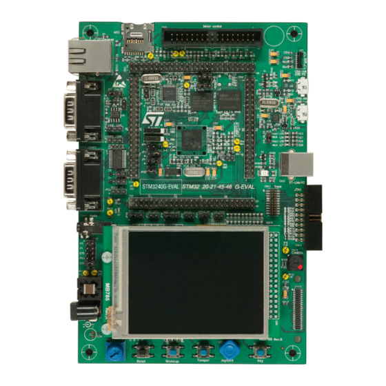
Figure 1. STM3240G-EVAL evaluation board
1. Picture is not contractual
October 2016
DocID022138 Rev 5
1/67
www.st.com
1
Advertisement
Table of Contents

Related Manuals for ST STM3240G-EVAL


Summary of Contents for ST STM3240G-EVAL
- Page 1 (USB-OTG HS, USB-OTG FS, Ethernet, motor control, CAN, microSD™ card, smartcard, USART, Audio DAC, RS-232, IrDA up to version C07 of the board, SRAM, ST MEMS, EEPROM etc.) before developing applications. Extension headers are used to easily connect a daughterboard or a wrapping board for any specific application.
-
Page 2: Table Of Contents
ST MEMS ........ - Page 3 STM3240G-EVAL pinout ........38...
- Page 4 STM3240G-EVAL pinout ........
- Page 5 STM3240G-EVAL evaluation board layout ........
-
Page 6: Overview
Demonstration software is preloaded in the board's Flash memory for easy demonstration of the device peripherals in standalone mode. For more information and to download the latest version, please refer to STM3240G-EVAL demonstration software available on the web at www.st.com/mcu... -
Page 7: Ordering Information
The plastic protection on the camera should be removed carefully as the connection is very fragile. Hardware layout and configuration The STM3240G-EVAL evaluation board is designed around the STM32F407IGH6 in the UFBGA176 package. The hardware block diagram Figure 2... -
Page 8: Figure 2. Hardware Layout And Configuration
Hardware layout and configuration UM1461 Figure 2. Hardware layout and configuration 2. The IrDA transceiver is present up to version C07 of the board 8/67 DocID022138 Rev 5... -
Page 9: Figure 3. Stm3240G-Eval Evaluation Board Layout
UM1461 Hardware layout and configuration Figure 3. STM3240G-EVAL evaluation board layout 3. IrDA is not populated on the board from version C08 of the board DocID022138 Rev 5 9/67... -
Page 10: Power Supply
UM1461 Power supply The STM3240G-EVAL evaluation board is designed to be powered by 5 V DC power supply and to be protected by PolyZen from a wrong power plug-in event. It is possible to configure the evaluation board to use any of following five sources for the power supply: •... -
Page 11: Boot Option
JP19 To connect Vbat to 3.3V power, set JP19 as shown: (Default setting) Note: LED LD9 is lit when the STM3240G-EVAL evaluation board is correctly 5V powered. Boot option The STM3240G-EVAL evaluation board is able to boot from: • Embedded user Flash •... -
Page 12: Clock Source
X4, 25 MHz crystal with socket for the,STM32F407IGH6 microcontroller (it can be removed from socket when internal RC clock is used) Reset source The reset signal of the STM3240G-EVAL evaluation board is low active and the reset sources include: •... -
Page 13: Eeprom
JP24 Default Setting: Not fitted The STM3240G-EVAL evaluation board enables two channels of CAN2.0A/B compliant CAN bus communication based on a 3.3V CAN transceiver on one DB9 connector (CN10). The two CAN buses can be disconnected by jumpers from relevant STM32F407IGH6 I/Os which are shared with FSMC and USB-OTG HS. -
Page 14: Table 7. Rs-232 And Irda Related Jumper
(CN16) and IrDA transceiver U11 which are connected to USART3 of the STM32F407IGH6 on the STM3240G-EVAL evaluation board. The IrDA transceiver (TFDU6300) is not populated on STM3240G-EVAL evaluation board from version C08. The version of the board is written on sticker on the bottom side of the board (ex: MB786-C08). -
Page 15: Motor Control
Hardware layout and configuration Motor control The STM3240G-EVAL evaluation board enables a three-phase brushless motor control via a 34- pin connector (CN5), which provides all required control and feedback signals to and from the motor power-driving board. Available signals on this connector include emergency... -
Page 16: Rs-232 And Irda
Hardware layout and configuration UM1461 2.10 Smartcard STMicroelectronics smartcard interface chip ST8024 is used on the STM3240G-EVAL board for asynchronous 3V and 5V smartcards. It performs all supply protection and control functions based on the connections with the STM32F407IGH6 listed in Table Table 9. -
Page 17: St Mems
USB connection at 5V DC with a 500 mA current limitation. The LED LD6 indicates that the power switch (U1) is ON and STM3240G-EVAL functions as a USB host or that the VBUS is powered by another USB host while STM3240G-EVAL functions as a USB device. -
Page 18: Usb-Otg Hs
VBUS. The evaluation board can be powered by this USB connector (CN9) at 5V DC with a 500 mA current limitation. LED LD7 indicates that power switch (U4) is ON and the STM3240G-EVAL is working as a USB host or that VBUS is powered by another USB host when the STM3240G-EVAL is working as a USB device. -
Page 19: Camera Module
UM1461 Hardware layout and configuration 2.18 Camera module A camera module is connected to the STM32F407IGH6 DCMI bus and shares the same I/Os with the motor control connector. SB16 must be kept open for camera module application. There are two possible modules and omnivision cameras populated on the CN15 connector of the board: •... -
Page 20: Sram
Hardware layout and configuration UM1461 The camera extension connector CN23 is available on the boards to connect the ST camera plug-in board. 2.19 SRAM The 16 Mbit SRAM is connected to the STM32F407IGH6 FSMC bus which shares the same I/Os with the CAN1 bus. JP3 and JP10 must not be fitted for SRAM and LCD application. - Page 21 Orange On: Communication failure Note: It is possible to power the board via CN21 (embedded ST-LINK/V2 USB connector) even if an external tool is connected to CN13 (trace) or CN14 (external JTAG and SWD). If the I2S interface is used, refer to the warning in Chapter 2.5.
-
Page 22: Display And Input Devices
Hardware layout and configuration UM1461 2.21 Display and input devices The 3.2” TFT color LCD connected to FSMC bus and 4 general purpose color LEDs (LD 1, 2, 3, 4) are available as display devices. A touchscreen connected to an I/O expander (U24), 4-direction joystick with selection key, general purpose button (B4), wakeup button (B2) and tamper detection button (B3) are available as input devices. -
Page 23: Connectors
Daughterboard extension connectors CN1, 2, 3 and 4 Four male headers, CN1, 2, 3 and 4, can be used to connect with a daughterboard or standard wrapping board to the STM3240G-EVAL evaluation board. A total number of 140 GPIOs are available on the board. - Page 24 Connectors UM1461 Table 18. Daughterboard extension connector CN1 (continued) How to disconnect with function block on Pin Description Alternative function STM3240G-EVAL board 49 EMU_5V Trace_CLK Trace_D1 & Keep JP1 on 2<->3 FSMC_A20 Trace_D3 PC13 Anti-Tamper Remove R143 10 GND 12 PI9...
-
Page 25: Table 19. Daughterboard Extension Connector Cn2
UM1461 Connectors Table 19. Daughterboard extension connector CN2 How to disconnect with function block on Pin Description Alternative function STM3240G-EVAL board ULPI_D0 ULPI_CLK Remove R69 MII_RX_DV Remove RS2, JP8 open MII_RXD1 Remove R58 11 PB0 ULPI_D1 13 PB2 BOOT1 15 PF12... -
Page 26: Table 20. Daughterboard Extension Connector Cn3
Connectors UM1461 Table 19. Daughterboard extension connector CN2 (continued) How to disconnect with function block on Pin Description Alternative function STM3240G-EVAL board 30 GND 32 PB10 ULPI_D3 34 PH6 MII_RXD2 Remove RS5 DCMI_HSYNC & Remove camera module from CN15. Disconnect motor 36 PH8 control board from CN5. - Page 27 UM1461 Connectors Table 20. Daughterboard extension connector CN3 (continued) How to disconnect with function block on Pin Description Alternative function STM3240G-EVAL board ULPI_D6 & PB13 CAN2_TX Remove camera module from CN15. DCMI_D3 & PH12 Disconnect motor control board from CN5.
-
Page 28: Table 21. Daughterboard Extension Connector Cn4
Connectors UM1461 Table 20. Daughterboard extension connector CN3 (continued) How to disconnect with function block on Pin Description Alternative function STM3240G-EVAL board APP_3V3 Table 21. Daughterboard extension connector CN4 How to disconnect with function block on Pin Description Alternative function STM3240G-EVAL board Remove camera module from CN15. - Page 29 UM1461 Connectors Table 21. Daughterboard extension connector CN4 (continued) How to disconnect with function block on Pin Description Alternative function STM3240G-EVAL board FSMC_BL1 I2C1_SDA Remove R111 FSMC_NL ULPI_D7 & JP10 open CAN2_RX TDO/SWO PG14 MII_TXD1 Remove RS6 PG13 MII_TXD0 Remove RS6...
-
Page 30: Motor Control Connector Cn5
Connectors UM1461 Motor control connector CN5 Figure 5. Motor control connector CN5 Table 22. Motor control connector CN5 STM32F407IGH6 STM32F407IGH6 Description CN5 pin CN5 pin Description EMERGENCY STOP PWM-UH PWM-UL PH13 PWM-VH PWM-VL PH14 PWM-WH PWM-WL PH15 VOLTAGE PHASE A CURRENT PHASE B CURRENT... -
Page 31: Microsd Connector Cn6
UM1461 Connectors microSD connector CN6 Figure 6. microSD connector CN6 Table 23. microSD connector CN6 Description Description SDIO_D2 (PC10) SDIO_CLK (PC12) SDIO_D3 (PC11) Vss/GND SDIO_CMD (PD2) SDIO_D0 (PC8) +3V3 SDIO_D1 (PC9) MicroSDcard_detect (PH13) Ethernet RJ45 connector CN7 Figure 7. Ethernet RJ45 connector CN7 Table 24. -
Page 32: Usb-Otg Fs Micro-Ab Connector Cn8
Connectors UM1461 USB-OTG FS Micro-AB connector CN8 Figure 8. USB-OTG FS Micro-AB connector CN8 Table 25. USB-OTG FS Micro-AB connector CN8 Description Description VBUS (PA9) ID (PA10) D- (PA11) D+ (PA12) USB-OTG HS Micro-AB connector CN9 Figure 9. USB-OTG HS Micro-AB connector CN9 Table 26. -
Page 33: Can D-Type 9-Pin Male Connectors Cn10 (Can1 Or Can2)
CANH 3,5,6 CANL Audio connector CN11 A 3.5mm stereo audio jack CN11 is available on the STM3240G-EVAL board to support a headset (headphone & microphone integrated). Trace debugging connector CN13 Figure 11. Trace debugging connector CN13 Table 28. Trace debugging connector CN13... -
Page 34: Jtag Debugging Connector Cn14
Connectors UM1461 Table 28. Trace debugging connector CN13 (continued) Description Description TraceD1/PE4 or nTRST/PB4 TraceD2/PE5 TraceD3/PE6 3.10 JTAG debugging connector CN14 Figure 12. JTAG debugging connector CN14 Table 29. JTAG debugging connector CN14 Description Description 3.3V power 3.3V power PA15 PA13 PA14 RTCK... -
Page 35: Camera Module Connector Cn15
UM1461 Connectors 3.11 Camera module connector CN15 Figure 13. Camera module connector CN15 (front view) Table 30. Camera module connector CN15 Description Description DGND XCLK1 DGND Y6(PI6) SIO_D (PB9) DGND AVDD (2.8V) Y5(PI4) SIO_C (PB6) PCLK (PA6) RESET Y4(PH14) VSYNC (PI5) Y0 (PH9) PWDN Y3(PH12) -
Page 36: Power Connector Cn18
RS232_TX (PC10) Bootloader_RESET 3.13 Power connector CN18 The STM3240G-EVAL evaluation board can be powered by a 5 V DC power supply via the external power supply jack (CN18) shown in Figure 15. CN18 central pin must be positive. Figure 15. Power supply connector CN18 3.14... -
Page 37: St-Link/V2 Connector Cn21
Description Card presence detection pin Card presence detection pin 3.16 ST-LINK/V2 connector CN21 The USB type B connector CN21 is intended for ST-LINK/V2 to connect between the STM3240G-EVAL evaluation board and the PC for board debugging. DocID022138 Rev 5 37/67... -
Page 38: Camera Extension Connector Cn23
DCMI_D4 DCMI_D5 DCMI_D6 DCMI_D7 HSYSC VSYSC PIXCLK +2V8 +2V8 3.18 STM3240G-EVAL pinout Table 34. STM3240G-EVAL pinout Pin name Description TRACE_CLK / FSMC_A23 TRACE_D0 / FSMC_A19 TRACE_D1 / FSMC_A20 TRACE_D2 / FSMC_A21 TRACE_D3 / FSMC_A22 VBAT VBAT PI8- ANTI TAMP2 LCD_HSYNC... - Page 39 UM1461 Connectors Table 34. STM3240G-EVAL pinout (continued) Pin name Description PC14-OSC32_IN 32K_OSC PC15-OSC32_OUT 32K_OSC LED2 PI10 ETHER_RX_ER PI11 USB_HS_DIR VSS_13 VDD_13 FSMC_A0 FSMC_A1 FSMC_A2 FSMC_A3 FSMC_A4 FSMC_A5 VSS_5 VDD_5 SmartCard_OFF SmartCard_RESET LCD_CS POTENTIOMETER PF10 Audio_IN PH0 - OSC_IN OSC_IN PH1 - OSC_OUT...
- Page 40 Connectors UM1461 Table 34. STM3240G-EVAL pinout (continued) Pin ne6032mrei ETHER_COL USB_HS_NXT USB_FS_POWER_ON USB_HS_D0 BYPASS BYPASS VDD_4 Audio_DAC_OUT USB_HS_CK CAM_PIXCK ETHER_DV ETHER_RXD0 / MC_ADC12_14 pin 14 (Bus voltage) ETHER_RXD1 / MC_ADC12_15 pin 26 (Heatsink temperature) USB_HS_D1 USB_HS_D2 BOOT1 / PF11 USB_FS_OVERCURRENT...
- Page 41 UM1461 Connectors Table 34. STM3240G-EVAL pinout (continued) Pin name Description PE15 FSMC_D12 PB10 USB_HS_D3 PB11 ULPI_D4 VCAP1 VCAP / 1.2V VDD_1 ETHER_RXD2 ETHER_RXD3 CAM_HSYNC / MC_NTC_bypass CAM_D0 PH10 CAM_D1 / MC_TIM5_ETR pin 27 (PFC SYNC) PH11 CAM_D2 / MC_TIM3_CH2 pin 27 (PFCSYNC)
- Page 42 Connectors UM1461 Table 34. STM3240G-EVAL pinout (continued) Pin name Description VDD_9 SmartCard_IO / Audio_I2S_ MCK LED3 SDIO_D0/ MC_TIM3_CH3 pin23 (Dissipative Brake) SDIO_D1 I2S_CKIN USB_FS_VBUS PA10 USB_FS_ID PA11 USB_FS_DM PA12 USB_FS_DP PA13 JTAG_TMS VCAP2 VCAP / 1.2V VSS 2 VDD_2 PH13...
- Page 43 UM1461 Connectors Table 34. STM3240G-EVAL pinout (continued) Pin name Description VDD_10 FSMC_NWAIT FSMC_NE1 FSMC_NE2 PG10 FSMC_NE3 PG11 ETHER_TXEN PG12 SmartCard_CMDVCC PG13 ETHER_TXD0 PG14 ETHER_TXD1 VSS_11 VDD_11 PG15 USER_BUTTON JTAG_TDO JTAG_TRST CAN2_RX / ETHER_PPS_OUT / ULPI_D7 I2C1_SCL FSMC_NL BOOT0 BOOT0 ETHER_TXD3 / MC_TIM4_CH3 pin 34 (Index)
-
Page 44: Appendix A Schematics
Schematics UM1461 Appendix A Schematics Appendix A contains the schematic diagrams listed below: • Figure 17: STM3240G-EVAL on page 45 • Figure 18: MCU on page 46 • Figure 19: USB-OTG HS on page 47 • Figure 20: Camera on page 48 •... - Page 45 Figure 17. STM3240G-EVAL U_Audio U_USB_OTG_HS Audio_IN I2S_MCK I2S_MCK ULPI_D[0..7] ULPI_D[0..7] Audio.SchDoc USB_OTG_HS.SchDoc I2S_CKIN Audio_RST Audio_IN ULPI_STP ULPI_STP U_MCU Audio_SDA I2S_CKIN RESET# MCU.SchDoc Audio_SCL I2S_SCK I2S_SCK ULPI_NXT ULPI_NXT I2S_SD I2S_SD ULPI_DIR ULPI_DIR I2S_WS I2S_WS ULPI_CLK ULPI_CLK Audio_DAC_OUT Audio_DAC_OUT U_USB_OTG_FS USB_OTG_FS.SchDoc OTG_FS_PowerSwitchOn...
- Page 46 Figure 18. MCU ULPI_D[0..7] ULPI_D[0..7] TP14 IOs Multiplexed U16A IOs Multiplexed MCO1 PTP_PPS PE15 WAKEUP PE15 PE14 U16B MII_RX_CLK/RMII_REF_CLK PE14 PE13 MII_MDIO PE13 VDD_MCU VDD_SA ULPI_D0 PE12 CAN2_RX PE12 PE11 +3V3 Audio_DAC_OUT PE11 PE10 MII_TXD3 ULPI_CLK PE10 MC_EnIndex DCMI_PIXCK SB10 MII_RX_DV/RMII_CRSDV Optional 100nF...
- Page 47 Figure 19. USB-OTG HS +3V3 +3V3 +3V3 Green FAULT R207 9013 4.7uF STMPS2141STR@54 ULPI_NXT PSW_N PI11 R206 ULPI_DIR FAULT [N/A] ULPI_STP RREF 12K[1%] VBUS_HS 475900001 ULPI_CLK CLOCK VBUS VBUS ULPI_D[0..7] ULPI_D7 ULPI_D[0..7] PB13 ULPI_D6 PB12 ULPI_D5 +3V3 PB11 ULPI_D4 VCC(I/O) PB10 ULPI_D3 VCC(I/O)
- Page 48 Figure 20. Camera +2V5 Camera_CLK CN23 R130 C149 CLM-120-02-L-D C150 SM7745HEW-24.0M CN15 +2V8 0.1uF 0.1uF XCLK1 AVDD(2.8V) +1V8 +1V8 PIXCLK +2V8 DCMI_PIXCK PCLK DVDD(1.8V) +1V8 VSYSC DCMI_VSYNC VSYNC DOVDD(2.8V) +2V8 HSYSC DCMI_HSYNC HREF DCMI_D[0..7] DCMI_D0 R213 DCMI_D[0..7] PH10 DCMI_D1 0.1uF 0.1uF 0.1uF 11 12...
- Page 49 Figure 21. Ethernet MII_CRS PI10 MII_RX_ER MII_COL MII_RXD3 +3V3 MII_RXD2 MII_TXD3 +3V3 MII_TXD2 MII_TX_CLK 1.5K 0.1uF 0.1uF Unused in RMII mode TX_CLK PG11 MII_TX_EN TX_EN PG13 MII_TXD0 TXD_0 PG14 MII_TXD1 TXD_1 TXD_2 TXD_3/SNI_MODE MII_RXD1 RXD_0/PHYAD1 MII_RXD0 RXD_1/PHYAD2 LED(green)_A MII_RX_DV/RMII_CRSDV RXD_2/PHYAD3 LED(green)_K RXD_3/PHYAD4 LED(Yellow)_A...
- Page 50 Figure 22. Audio Nokia Nokia R110 R112 0.022uF 0.022uF CN11 Audio_SDA HP/LINE_OUTA Audio_SCL HP/LINE_OUTB SPKR/HP I2S_MCK MCLK PJ3028B-3 I2S_SCK SCLK SPKR_OUTA+ R134 I2S_SD SDIN SPKR_OUTA- I2S_WS LRCK SPKR_OUTB+ KSS-1508 or KSSG1708 Audio_RST RESET SPKR_OUTB- From IO expandor R215 R216 R217 R218 -VHPFILT [N/A]...
- Page 51 Figure 23. USB-OTG FS +3V3 +3V3 OTG_FS_OverCurrent PF11 FAULT VBUS OTG_FS_PowerSwitchOn STMPS2141STR@54 4.7uF Shield 475900001 +3V3 VBUS_FS PA11 OTG_FS_DM PA12 OTG_FS_DP PA10 OTG_FS_ID Green Vbus D+out D+in D-out D-in R180 9013 R181 EMIF02-USB03F2 [N/A] Title: STM32 20-21-45-46 G-EVAL USB_OTG_FS Number: MB786 Rev: C.3(PCB.SCH)
- Page 52 Figure 24. SRAM D[0..15] D[0..15] A[0..20] A[0..20] I/O15 I/O14 I/O13 I/O12 I/O11 I/O10 I/O9 I/O8 DQ10 I/O7 DQ11 I/O6 DQ12 +3V3 I/O5 DQ13 I/O4 DQ14 I/O3 DQ15 I/O2 I/O1 VccIO R52 0 +3V3 I/O0 VccCore +3V3 +3V3 100nF 100nF 100nF R47 0 FSMC_NE2 100nF...
- Page 53 Figure 25. LCD D[0..15] D[0..15] A[0..20] A[0..20] CN19 PG10 FSMC_NE3 R119 R161 R162 R163 FSMC_NWE WR/SCL R164 R165 FSMC_NOE R166 RESET# RESET R167 R168 R169 R170 PD10 R171 BL_GND PD11 R172 BEAD BL_Control PD12 R173 +3V3 PD13 R174 PD14 R175 PD15 C153 C148...
- Page 54 Figure 26. RS-232 and IrDA +3V3 100nF CN16 100nF DB9-male UART3 or 4 100nF 100nF 100nF T1IN T1OUT PC10 RS232/IrDA_TX T2IN T2OUT T3IN T3OUT R1OUTB Bootloader_BOOT0 R2OUTB R1OUT R1IN R2OUT R2IN R3OUT R3IN PC11 RS232/IrDA_RX Bootloader_RESET R4OUT R4IN R5OUT R5IN +3V3 JP22 nSHDN...
- Page 55 Figure 27. CAN +3V3 +3V3 CN10 Default setting: 1<->2 DB9-male CAN connector Default setting: Open 100nF CAN1_TX PB13 CAN2_TX CANH CANL Vref SN65HVD230 CAN1_RX CAN2_RX JP10 do not fit +3V3 Title: STM32 20-21-45-46 G-EVAL CAN Number: MB786 Rev: C.3(PCB.SCH) Date: 7/20/2016 Sheet...
- Page 56 Figure 28. I/O peripherals Green R155 LED1 Orange R154 LED2 R141 LED3 Blue R140 LED4 Title: Number: Rev: C.3(PCB.SCH) Date: 7/20/2016 Sheet...
- Page 57 Figure 29. I/O expander +2V8 100nF TouchScreen_Y- TouchScreen_X- TouchScreen_Y+ IO_Expandor_SCK SCLK TouchScreen_X+ IO_Expandor_SDA SDAT EXP_IO9 R136 IO_Expandor_INT EXP_IO10 Data in EXP_IO11 A0/Data Out EXP_IO12 R117 STMPE811QTR I2C device address:0x82 R116 100K +2V8 +2V8 C115 100nF EXP_IO1 EXP_IO2 EXP_IO3 SCLK EXP_IO4 SDAT EXP_IO5 EXP_IO6...
- Page 58 Figure 30. microSD card +3V3 +3V3 MicroSDCard_D1 MicroSDCard_D0 PC11 MicroSDCard_D3 PC10 MicroSDCard_D2 PC12 MicroSDCard_CLK MicroSDCard_CMD PJS008-2000 SMS064FF or SMS128FF PH13 MicroSDCard_Detect MicroSD card Title: STM32 20-21-45-46 G-EVAL MicroSD card Number: MB786 Rev: C.3(PCB.SCH) Date: 7/20/2016 Sheet...
- Page 59 Figure 31. Motor control +3V3 Motor control connector 3.3K MC_EmergencySTOP EMERGENCY STOP MC_UH MC-UH PH13 MC_UL MC_UL AIN- AIN+ MC_VH MC_VH PH14 MC_VL MC_VL MC_WH MC_WH PH15 MC_WL MC_WL BUS VOLTAGE MC_BusVoltage R219 MC_CurrentA CURRENT A R74 0 CURRENT B 100nF 100K CURRENT C...
- Page 60 Figure 32. Smartcard +3V3 +3V3 R124 R125 R157 PH15 SmartCard_3/5V TP11 AUX2 CLKDIV1 AUX2UC TP12 CLKDIV2 AUX1UC R127 AUX1 5V/3V I/OUC SmartCard_IO PGND XTAL2 C125 100nF XTAL1 SmartCard_CLK R126 Vddp SmartCard_OFF C117 C126 C127 100nF 47uF +3V3 100nF PRES RSTIN C114 R128 C111...
- Page 61 Figure 33. JTAG and Trace +3V3 R101 [N/A] [N/A] [N/A] [N/A] PA13 TMS/SWDIO PA14 TCK/SWCLK TDO/SWO PA15 TRST RESET# [N/A] CN13 FTSH-110-01-L-DV CN14 +3V3 JTAG +3V3 +3V3 do not fit R104 0 R100 do not fit R94 0 R91 do not fit R105 R106 JTAG connector...
- Page 62 Figure 34. Power ZEN056V130A24LS +3V3 VDD_MCU CN18 JP32 C106 10uF DC-10B SMAJ5.0A-TR C112 VBUS_HS 100nF BNX002-01 JP18 VBUS_FS TP13 Ground TP10 U5V_ST_LINK LD1086D2M33TR +3V3 LD1117S18TR LD1117STR +2V8 Header 5X2 Vout Vout +1V8 Vout C113 R114 220uF 220uF 10uF C116 100nF 10uF C110 10uF...
- Page 63 Figure 35. Extension connector 21N22564-50S10B PA14 PA15 PB11 PB10 21N22564-50S10B 21N22564-40S10B 21N22564-40S10B RESET# RESET# Title: STM32 20-21-45-46 G-EVAL Extension connector Number: MB786 Rev: C.3(PCB.SCH) Date: 7/20/2016 Sheet...
- Page 64 Figure 36. STLINK/V2 +3V3 LED_STLINK C134 C135 C136 C133 100nF 100nF 100nF 100nF R201 +3V3 R185 R186 +3V3 STM32F103C8T6 C138 C139 20pF 20pF AIN_1 +3V3 +3V3 8MHz VBAT VDD_2 PC13 VSS_2 STM_JTMS_SWDIO PC14 JTMS USB_DP PC15 PA12 OSC_IN USB_DM OSC_IN PA11 OSC_OUT OSC_OUT...
- Page 65 Figure 37. 3.2” LCD module with SPI and 16-bit interface Soldered for i80-system 16-bit interface WR/SCL #RESET RESET BLGND PD10 PD10 PD11 BL_GND PD11 BL_Control PD12 BL_Control PD12 PD13 Soldered for Serial interface only PD13 PD14 PD14 PD15 PD15 PD16 PD16 PD17 VSYNC...
-
Page 66: Revision History
Revision history UM1461 Revision history Table 35. Document revision history Date Revision Changes 02-Sept-2011 Initial release. Updated Table 5 JP24 description. Added warning in Chapter 2.5 09-Oct-2011 note in Chapter 2.16 Chapter 2.20. Added note in Chapter 2.5 and updated Chapter Appendix A: 09-Jan-2012 Schematics. - Page 67 ST products and/or to this document at any time without notice. Purchasers should obtain the latest relevant information on ST products before placing orders. ST products are sold pursuant to ST’s terms and conditions of sale in place at the time of order acknowledgement.
Need help?
Do you have a question about the STM3240G-EVAL and is the answer not in the manual?
Questions and answers