Table of Contents
Advertisement
Introduction
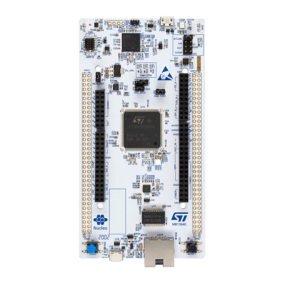
The STM32H7 Nucleo-144 boards based on the MB1364 reference board (NUCLEO-
H723ZG, NUCLEO-H743ZI (Order code NUCLEO-H743ZI2), and NUCLEO-H753ZI)
provide an affordable and flexible way for users to try out new concepts and build
prototypes, by choosing from the various combinations of performance and power
consumption features provided by the STM32H7 Series microcontroller. The ST Zio
connector, which extends the ARDUINO
provide an easy means of expanding the functionality of the Nucleo open development
platform with a wide choice of specialized shields. The STM32H7 Nucleo-144 boards do not
require any separate probe as they integrate the STLINK-V3 debugger/programmer. The
STM32H7 Nucleo-144 boards come with the comprehensive free software libraries and
examples available with the STM32Cube MCU Package.
Figure 1. Nucleo-144 board (top view)
Pictures are not contractual.
June 2020
STM32H7 Nucleo-144 boards (MB1364)
®
Uno V3 connectivity, and the ST morpho headers
Figure 2. Nucleo-144 board (bottom view)
UM2407 Rev 2
UM2407
User manual
www.st.com
1/50
1
Advertisement
Table of Contents


Need help?
Do you have a question about the STM32H7 Nucleo-144 and is the answer not in the manual?
Questions and answers