Table of Contents
Advertisement
Advertisement
Table of Contents

Related Manuals for Motorola MVME2100


Summary of Contents for Motorola MVME2100
- Page 1 MVME2100 Single Board Computer Installation and Use V2100A/IH2 July 2001 Edition...
- Page 2 Motorola and the Motorola symbol are registered trademarks of Motorola, Inc. PowerPC and the PowerPC logo are registered trademarks of International Business Machines Corporation and are used by Motorola, Inc. under license from International Business Machines Corporation. PC•MIP is a trademark of SBS GreenSpring Modular I/O, Inc.
- Page 3 The safety precautions listed below represent warnings of certain dangers of which Motorola is aware. You, as the user of the product, should follow these warnings and all other safety precautions necessary for the safe operation of the equipment in your operating environment.
- Page 4 Flammability All Motorola PWBs (printed wiring boards) are manufactured with a flammability rating of 94V-0 by UL-recognized manufacturers. EMI Caution This equipment generates, uses and can radiate electromagnetic energy. It may cause or be susceptible to electromagnetic interference (EMI) if not installed and used with adequate EMI protection.
- Page 5 While reasonable efforts have been made to assure the accuracy of this document, Motorola, Inc. assumes no liability resulting from any omissions in this document, or from the use of the information obtained therein. Motorola reserves the right to revise this document and to make changes from time to time in the content hereof without obligation of Motorola to notify any person of such revision or changes.
- Page 6 If the documentation contained herein is supplied, directly or indirectly, to the U.S. Government, the following notice shall apply unless otherwise agreed to in writing by Motorola, Inc. Use, duplication, or disclosure by the Government is subject to restrictions as set forth in subparagraph (b)(3) of the Rights in Technical Data clause at DFARS 252.227-7013 (Nov.
-
Page 7: Table Of Contents
PCI Mezzanine Cards (PMCs)................1-2 PC•MIP Expansion .....................1-2 VME System Enclosure..................1-3 System Console Terminal ...................1-3 Unpacking the MVME2100 Hardware ..............1-4 Preparing the MVME2100 Hardware ................1-4 MVME2100 Configuration Settings..............1-4 Setting Flash Memory Bank A/Bank B Header (J9) (Pins 1 and 2)....1-5 Setting System Controller Selection Header (J2) ........1-5 PMCs ........................1-6... - Page 8 Switches......................2-3 ABT (S1) ..................... 2-3 RST (S2)...................... 2-4 BFL (DS1)....................2-4 SYS (DS2)....................2-4 RUN (DS3)....................2-4 10/100 BASE T Port................... 2-4 DEBUG Port....................... 2-4 Jumper Settings ....................2-6 I/O Expansion Cards ..................2-7 PCI Mezzanine Card ................... 2-7 TYPE II PC-MIP..................
- Page 9 Configuring the PPCBug Parameters ..............5-3 LED/Serial Startup Diagnostic Codes ............5-11 Configuring the VMEbus Interface ..............5-12 Firmware Command Buffer...............5-16 APPENDIX A Related Documentation Motorola Computer Group Documents ..............A-1 Manufacturers’ Documents..................A-2 Related Specifications....................A-5 APPENDIX B Specifications Specifications ......................B-1 Mechanical Characteristics ................B-1 Electrical Characteristics ...................
- Page 10 APPENDIX C Connector Pin Assignments Introduction ......................C-1 VMEbus Connectors ..................C-1 PC•MIP PCI Interface Connectors ..............C-3 PC•MIP User Defined I/O Connectors.............. C-5 PCI Mezzanine Card (PMC) PCI Interface Connectors........C-6 PMC User Defined I/O Connector ..............C-8 PCI Expansion Connector ................ C-10 10BaseT/100BaseTx Connector...............
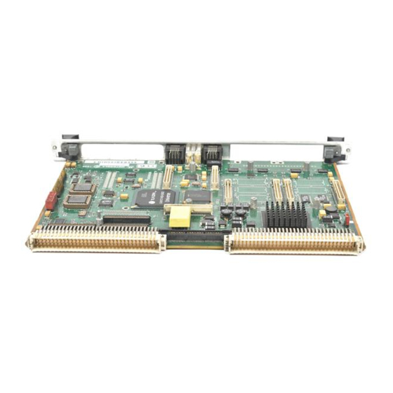
- Page 11 List of Figures Figure 1-1. MVME2100 Layout ................1-7 Figure 1-2. MVME2100 Installation and Removal From a VMEbus Chassis ..1-9 Figure 1-3. Typical Single-width PMC Module Placement on an MVME2100 ..1-10 Figure 1-4. Typical Type II PC•MIP Placement on an MVME2100 .......1-11 Figure 1-5.
- Page 13 Table A-1. Motorola Computer Group Documents ..........A-1 Table A-2. Manufacturers’ Documents ..............A-2 Table A-3. Related Specifications ................A-5 Table B-1. Power Requirements for the MVME2100 ..........B-1 Table B-2. MVME2100 Environmental Specifications ........... B-2 Table B-3. Thermally Significant Components ............B-5 Table C-1.
- Page 15 MVME2100 Single Board Computer. It provides specific preparation and installation information and data applicable to the board. As of the printing date of this manual, the MVME2100 is available in the configurations shown below. Model...
-
Page 16: Summary Of Changes
Description, provides an explanation of the functional components on the MVME2100. The chapter includes a listing of the MVME2100 features and a block diagram. The remainder of the chapter includes specific descriptions of each functional element on the board and a description of its functional characteristics. -
Page 17: Comments And Suggestions
Chapter 5, Modifying the Environment, describes how to change certain parameters of the MVME2100 board by using the CNFG and ENV commands of the PPCBug firmware. Appendix A, Related Documentation, provides a listing of other Motorola documents related to the MVME2100, as well as manufacturer’s documents dealing with specific components on the board. -
Page 18: Conventions Used In This Manual
Conventions Used in This Manual The following typographical conventions are used in this document: bold is used for user input that you type just as it appears; it is also used for commands, options and arguments to commands, and names of programs, directories and files. - Page 19 An asterisk (*) following a signal name for signals that are edge significant denotes that the actions initiated by that signal occur on high to low transition. In this manual, assertion and negation are used to specify forcing a signal to a particular state.
-
Page 21: Introduction
Unless otherwise specified, the designation “MVME2100” refers to all models of the MVME2100-series single board computers. The MVME2100 SBC is installed in a standard VME chassis and uses injector/ejector handles for easy installation and removal. A combination of PCI mezzanine cards (PMC) and PC Mezzaine Industry Pack (PC•MIP) I/O cards can be installed on the MVME2100. -
Page 22: Pmcspan Expansion Mezzanine
To maximize I/O expansion flexibility, the MVME2100 provides a combination of Type I and Type II PC•MIP slots for added capability. The MVME2100 provides one Type I PC•MIP slot with rear I/O via the P2 connector and two Type II PC•MIP slots with front panel I/O. The two Type II slots can accept either one double-wide or two single-wide PC•MIP cards. -
Page 23: Vme System Enclosure
Introduction VME System Enclosure Your MVME2100 board must be installed in a VME system chassis with both P1 and P2 backplane connections. It requires a single slot, except when PMCspan carrier boards are used. Allow one extra slot for each PMCspan. -
Page 24: Unpacking The Mvme2100 Hardware
To produce the desired configuration and ensure proper operation of the board, it may be necessary to perform certain modifications before and after installing it. The following paragraphs discuss the preparation of the MVME2100 hardware components prior to installing them into a chassis and connecting them. MVME2100 Configuration Settings The MVME2100 provides software control over most options by setting bits in control registers. -
Page 25: Setting Flash Memory Bank A/Bank B Header (J9) (Pins 1 And 2)
1 on the VME system, it configures itself as the system controller. Remove the jumper from J2 if you intend to operate the MVME2100 as system controller in all cases. -
Page 26: Pmcs
You will need to use an additional slot in the VME chassis for each PMCspan expansion module you plan to use. Before installing a PMCspan on the MVME2100, you must install the selected PMCs on the PMCspan. Refer to the PMCspan PMC Adapter Carrier Board Installation and Use manual for instructions. -
Page 27: Installing The Mvme2100 Hardware
Installing the MVME2100 Hardware Installing the MVME2100 Hardware The following section discusses installing PMCs and PMCspan modules onto the MVME2100, installing the MVME2100 into a VME chassis, and connecting an optional system console terminal. TYPE II PC•MIP SLOTS TYPE I I P C•MIP... -
Page 28: Esd Precautions
Note that a system chassis may not be grounded if it is unplugged. PMCs & PC•MIPs PMC modules and PC•MIP cards mount on top of the MVME2100 SBC. Perform the following steps to install a PMC module and/or a PC•MIP card on your MVME2100. -
Page 29: Figure 1-2. Mvme2100 Installation And Removal From A Vmebus Chassis
Remove chassis or system cover(s) as necessary for access to the VME modules. 3. If the MVME2100 has already been installed in a VMEbus card slot, carefully remove it as shown in the figure below and place it with connectors P1 and P2 facing you. -
Page 30: Figure 1-3. Typical Single-Width Pmc Module Placement On An Mvme2100
MVME2100’s mating connectors (J11/J12/J14), or if installing a PC•MIP, position the card’s mating connectors on top of the MVME2100’s Type II PC•MIP connectors (P41/P42 or P31/P32 for Type II; or P21/P22/P23 for Type I PC- MIP). -
Page 31: Primary Pmcspan
Installing the MVME2100 Hardware Figure 1-4. Typical Type II PC•MIP Placement on an MVME2100 6. Insert the appropriate number of Phillips head screws (typically 2) through the holes of the PMC module or PC•MIP card(s), into the mating standoffs on the MVME2100 and tighten the screws. - Page 32 Remove chassis or system cover(s) as necessary for access to the VME module card cage. 3. If the MVME2100 has already been installed in the chassis, carefully remove it from the VMEbus card slot and position it with connectors P1 and P2 facing you.
-
Page 33: Figure 1-5. Pmcspan-001 Installation On An Mvme2100
Installing the MVME2100 Hardware PMCspan MVME2100 2081 9708 Figure 1-5. PMCspan-001 Installation on an MVME2100 http://www.motorola.com/computer/literature 1-13... -
Page 34: Secondary Pmcspan
– Tighten the nuts with a box-end wrench or a pair of needle nose pliers. 5. Place the PMCspan on top of the MVME2100. Align the mounting holes to the standoffs in each corner, and align PMCspan connector P4 with MVME2100 connector J4. -
Page 35: Figure 1-6. Pmcspan-010 Installation On A Pmcspan-001/Mvme2100
Installing the MVME2100 Hardware 2065 9708 Figure 1-6. PMCspan-010 Installation on a PMCspan-001/MVME2100 http://www.motorola.com/computer/literature 1-15... - Page 36 Avoid touching areas of integrated circuitry; static discharge can damage these circuits. Caution 3. If the Primary PMC Carrier Module/MVME2100 assembly is already installed in the VME chassis, carefully remove the two- board assembly from the VMEbus card slots and position it with the P1 and P2 connectors facing you.
-
Page 37: Mvme2100 System Installation
PMCspan, above the card slot for the MVME2100. – If you intend to use the MVME2100 as the system controller, it must occupy the left-most card slot (slot 1). The system... - Page 38 Preparation and Installation – If you do not intend to use the MVME2100 as the system controller, it can occupy any unused card slot. 4. Slide the MVME2100 (and PMCspans if used) into the selected card slot(s). Be sure the module or modules is/are seated properly in the P1 and P2 connectors on the backplane.
-
Page 39: Installation Considerations
If the MVME2100 tries to access off-board resources that do not respond to its cycle, and the MVME2100 is not the system controller, and the system does not have a global bus time-out, the MVME2100 waits indefinately for the VMEbus cycle to complete. -
Page 41: Introduction
PPCBug firmware power-up or system reset. The firmware initializes the devices on the MVME2100 module in preparation for booting the operating system. The firmware is shipped from the factory with an appropriate set of defaults. -
Page 42: Figure 2-1. System Boot-Up Sequence
Operating Instructions Power-up/reset initialization STARTUP Initialize devices on the MVME2100 INITIALIZATION Power-On Self-Test diagnostics POST Firmware configured boot mechanism, BOOTING if so configured. Default is no boot. Interactive, command-driven on-line PowerPC MONITOR debugger, when terminal connected Figure 2-1. System Boot-up Sequence... -
Page 43: Mvme2100 User Interface Devices
MVME2100. These devices include MVME2100 switches and their settings, status indicators, the MVME2100 Debug port, the jumper settings, the MVME2100 I/O Expansion card openings and the PMCspan openings. Front panels are depicted on several of the following pages as an... -
Page 44: Rst (S2)
The green LED illuminates when either ROM/FLASH, SDRAM, or accesses are occurring 10/100 BASE T Port The RJ45 port on the front panel of the MVME2100 labeled 10/100 BASE supplies the Ethernet LAN 10BaseT/100BaseTx interface. DEBUG Port The RJ45 port labeled... - Page 45 Control Register (MISC_CTL) in the Universe ASIC. SYSRESET* remains asserted for at least 200 ms, as required by the VMEbus specification. port may be used for connecting a terminal to the MVME2100 DEBUG to serve as the firmware console for the factory installed debugger, PPCBug.
-
Page 46: Jumper Settings
Operating Instructions Jumper Settings The following table describes the MVME2100 jumper configuration. Table 2-1. Jumper Switches and Settings Jumper Description Setting Default Factory Test Header Reserved VMEbus System Pins 1 & 2 Shorted: Disables the System Controller Controller Function Shunt on... -
Page 47: I/O Expansion Cards
MVME2100 User Interface Devices I/O Expansion Cards Two openings are located on the front panel of the MVME2100 to provide I/O expansion by allowing access to a PCI Mezzanine Card (PMC) or two Type II PC•MIP cards. Refer to Appendix C, Connector Pin Assignments for additional information on pin assignments. -
Page 49: Chapter 3 Functional Description
This chapter provides additional product information along with a general functional description for the MVME2100 single board computer. The MVME2100 is a VME based single-slot single board computer based on the MPC8240 Integrated Processor. Key features of the MVME2100 include one 32-bit PMC expansion slot, one Type I and two Type II PC•MIP expansion slots, 32 or 64MB of... - Page 50 Functional Description Table 3-1. MVME2100 Features (Continued) • Integrated I C port with full master support • I O compliant messaging Interface NVRAM • 8KB (MK48T59Y) RTC & • MK48T59 device Watchdog Timer Serial Interface • One 16550-compatible async serial port PCI Mezzanine Card •...
-
Page 51: Figure 3-1. Mvme2100 Block Diagram
Debug Connector Flash Clock 5/9MB Generator 16550 DRAM 32/64MB MPC8240 EEPROM ETHERNET LXT970 DEC21143 PC•MIP TYPE II Slot 2 PC•MIP TYPE II Slot 1 Expansion Connector Slot PC•MIP TYPE I Slot 2 Universe II Figure 3-1. MVME2100 Block Diagram http://www.motorola.com/computer/literature... -
Page 52: Functional Description
MVME2100 and in some cases the corresponding functions associated with those components. Processor The MVME2100 is designed to support the MPC8240 processor in a 352 pin TBGA package. It is also designed to support memory bus speeds of 50, 60, 66.67, and 83.33 MHz. -
Page 53: Pci Local Bus
Functional Description Since the MVME2100 could have as many as seven potential PCI masters in addition to the processor, an onboard sub-arbiter is provided. The sub- arbiter is designed to multiplex the PMC slot and three PC•MIP slots onto one set of the processor’s PCI bus request/grant pins. -
Page 54: Two-Wire Serial Interface
Functional Description Two-Wire Serial Interface A two-wire serial interface for the MVME2100 is provided by an I compatible serial controller integrated into the processor’s peripheral device. The processor’s serial controller is used by the system software to read the contents of the configuration EEPROM contained on the board. -
Page 55: System Clock Generator
Flash Memory The MVME2100 contains two banks of Flash memory accessed via the integrated memory controller contained within the processor. Bank B consists of two 32-pin PLCC sockets that can be populated with up to 1024KB of Flash memory, and resides at address 0xFFF00000, and is restricted to 8 bits in width. -
Page 56: Ethernet Interface
Ethernet address is stored in the configuration ROM interfaced to the Ethernet controller. Asynchronous Serial Port The MVME2100 uses a TL16C550 or compatible Universal Asynchronous Receiver/Transmitter (UART) with a 1.8432 MHz input clock to provide an asynchronous serial interface. EIA232 drivers and receivers reside onboard and are routed to an industry standard RJ45 connector accessible from the front panel. -
Page 57: Vmebus Interface
Functional Description VMEbus Interface The VMEbus interface for the MVME2100 is provided by the Universe II ASIC. Refer to the Universe II User’s Manual, listed in Appendix A Related Documentation for additional information. PCI Mezzanine Card Slot The MVME2100 provides one PMC slot. Three EIA E700 AAAB connectors interface to a single 32-bit IEEE P1386.1 PMC to add any... -
Page 58: Pci/Pmc Expansion Capability
PMC boards can be used. Real-Time Clock & NVRAM The ST-Thomson M48T59 is used by the MVME2100 to provide 8KB of non-volatile static RAM and a real-time clock. It consists of two parts: A 28-pin 330mil SO device which contains the RTC, the oscillator, 8KB of SRAM, and gold-plated sockets for the SNAPHAT battery. -
Page 59: Ppcbug Overview
PPCBug Basics The PowerPC debug firmware (known as the “PPCBug”) is a powerful evaluation and debugging tool for systems built around the Motorola PowerPC microcomputers. Facilities are available for loading and executing user programs under complete operator control for system evaluation. - Page 60 PPCBug Firmware Package User’s Manual. It is hereafter referred to as “the debugger” or “PPCBug.” A command-driven diagnostics package for the MVME2100 hardware, hereafter referred to as “the diagnostics.” The diagnostics package is described in the PPCBug Diagnostics Manual.
-
Page 61: Memory Requirements
MPU, Hardware, and Firmware Initialization The debugger performs the MPU, hardware, and firmware initialization process. This process occurs each time the MVME2100 is reset or powered up. The steps below are a high-level outline; not all of the detailed steps are listed. - Page 62 PPCBug Firmware 8. Delays for 750 milliseconds. 9. Determines the CPU base board type. 10. Sizes the local read/write memory (i.e., DRAM). 11. Initializes the read/write memory controller. Sets base address of memory to 0x00000000. 12. Retrieves the speed of read/write memory. 13.
-
Page 63: Using Ppcbug
After the debugger executes the command, the prompt reappears. However, depending on what the user program does, if the command causes execution of a user target code (i.e., GO), then control may or may not return to the debugger. http://www.motorola.com/computer/literature... -
Page 64: Debugger Commands
PPCBug Firmware For example, if a breakpoint has been specified, then control returns to the debugger when the breakpoint is encountered during execution of the user program. Alternately, the user program could return to the debugger by means of the System Call Handler routine RETURN (described in the PPCBug Firmware Package User’s Manual, listed in Appendix A, Related Documentation). -
Page 65: Table 4-1. Debugger Commands
PCI Configuration Space WRITE Access Data Conversion and Expression Evaluation Disassembler Dump S-Records ECHO Echo String Set Environment to Bug/Operating System FORK Fork Idle MPU at Address FORKWR Fork Idle MPU with Registers “Alias” for “GO” Command Go Direct (Ignore Breakpoints) http://www.motorola.com/computer/literature... - Page 66 PPCBug Firmware Table 4-1. Debugger Commands (Continued) Command Description GEVBOOT Global Environment Variable Boot - Bootstrap Operating System GEVDEL Global Environment Variable Delete GEVDUMP Global Environment Variable(s) Dump (NVRAM Header + Data) GEVEDIT Global Environment Variable Edit GEVINIT Global Environment Variable Initialize (NVRAM Header) GEVSHOW Global Environment Variable Show...
- Page 67 Disable Macro Expansion Listing NOPA Printer Detach NOPF Port Detach NORB No ROM Boot NOSYM Detach Symbol Table NPING Network Ping Offset Registers Display/Modify Printer Attach PBOOT Bootstrap Operating System Port Format PFLASH Program FLASH Memory Put RTC into Power Save Mode http://www.motorola.com/computer/literature...
- Page 68 PPCBug Firmware Table 4-1. Debugger Commands (Continued) Command Description ROMboot Enable Register Display REMOTE Remote RESET Cold/Warm Reset Read Loop Register Modify Register Set MPU Execution/Status Switch Directories Set Time and Date SROM SROM Examine/Modify Symbol Table Attach SYMS Symbol Table Display/Search Trace Terminal Attach TIME...
-
Page 69: Diagnostic Tests
PPCBug’s diagnostic test groups are listed in Table 4-2. Note that not all tests are performed on the MVME2100. Using the HE command, you can list the diagnostic routines available in each test group. Refer to the PPCBug Diagnostics Manual listed in Appendix A,... -
Page 70: Table 4-2. Diagnostic Test Groups
Some diagnostics depend on restart defaults that are set up only in a particular restart mode. Refer to the documentation on a particular diagnostic for the correct mode. Test Sets marked with an asterisk (*) are not available on the MVME2100. 4-12 Computer Group Literature Center Web Site... -
Page 71: Overview
5Modifying the Environment Overview You can use the factory-installed debug monitor, PPCBug, to modify certain parameters contained in the MVME2100 Non-Volatile RAM (NVRAM), also known as Battery Backed-up RAM (BBRAM). The Board Information Block in NVRAM contains various elements concerning operating parameters of the hardware. Use the PPCBug command CNFG to change those parameters. -
Page 72: Cnfg - Configure Board Information Block
Use this command to display and configure the Board Information Block, which is resident within the NVRAM. This data block contains various elements detailing specific operational parameters of the MVME2100. The structure for the board is shown in the following example:... -
Page 73: Env - Set Environment
Refer to the PPCBug Firmware Package User’s Manual for a description of the use of ENV. Additional information on registers in the Universe ASIC that affect these parameters is contained in the MVME2100 Programmer’s Reference Guide listed in Appendix A, Related Documentation. - Page 74 Do not display the field service menu. (Default) Remote Start Method Switch [G/M/B/N] = B? The Remote Start Method Switch is used when the MVME2100 is cross-loaded from another VME-based CPU in order to start execution of the cross-loaded program.
- Page 75 SCSI Bus Reset on Debugger Startup [Y/N] = N? Local SCSI bus is reset on debugger setup. Local SCSI bus is not reset on debugger setup. (Default) Primary SCSI Bus Negotiations Type [A/S/N] = A? Asynchronous SCSI bus negotiation. (Default) Synchronous SCSI bus negotiation. None. http://www.motorola.com/computer/literature...
- Page 76 Modifying the Environment Primary SCSI Data Bus Width [W/N] = N? Wide SCSI (16-bit bus). Narrow SCSI (8-bit bus). (Default) Secondary SCSI identifier = 07? Select the identifier. (Default = 07.) NVRAM Bootlist (GEV.fw-boot-path) Boot Enable [Y/N] = N? Give boot priority to devices defined in the fw-boot- path global environment variable (GEV).
- Page 77 (1, 2, 3, 4) until it finds the first “bootable” partition. That is then the partition that will be booted. Other acceptable values are 1, 2, 3, or 4. In these four cases, the partition specified will be booted without searching. http://www.motorola.com/computer/literature...
- Page 78 Modifying the Environment Auto Boot Abort Delay = 7? The time in seconds that the Autoboot sequence will delay before starting the boot. The purpose for the delay is to allow you the option of stopping the boot by use of the key.
- Page 79 The address where the network interface configuration parameters are to be saved/retained in NVRAM; these parameters are the necessary parameters to perform an unattended network boot. A typical offset might be 0x1000, but this value is application-specific. Default = 0x00001000. http://www.motorola.com/computer/literature...
- Page 80 Modifying the Environment If you use the NIOT debugger command, these parameters need to be saved somewhere in the offset range 0x00001000 through 0x000016F7. The NIOT parameters do not exceed 128 bytes in Caution size. The setting of this ENV pointer determines their location. If you have used the same space for your own program information or commands, they will be overwritten and lost.
-
Page 81: Led/Serial Startup Diagnostic Codes
If the debugger fails to come up to a prompt, the last code displayed will indicate how far the initialization sequence had progressed before stalling. The codes are enabled by an ENV parameter similar to the following: http://www.motorola.com/computer/literature 5-11... -
Page 82: Configuring The Vmebus Interface
Configuring the VMEbus Interface ENV asks the following series of questions to set up the VMEbus interface for the MVME2100. To perform this configuration, you should have a working knowledge of the Universe ASIC as described in your MVME2100 Programmer’s Reference Guide. - Page 83 PCI Slave Image 3 Control = C0400000? The configured value is written into the LSI3_CTL register of the Universe chip. PCI Slave Image 3 Base Address Register = AFFF0000? The configured value is written into the LSI3_BS register of the Universe chip. http://www.motorola.com/computer/literature 5-13...
- Page 84 Modifying the Environment PCI Slave Image 3 Bound Address Register = B0000000? The configured value is written into the LSI3_BD register of the Universe chip. PCI Slave Image 3 Translation Offset = 50000000? The configured value is written into the LSI3_TO register of the Universe chip.
- Page 85 Special PCI Slave Image Register = 00000000? The configured value is written into the SLSI register of the Universe chip. Master Control Register = 80C00000? The configured value is written into the MAST_CTL register of the Universe chip. http://www.motorola.com/computer/literature 5-15...
-
Page 86: Firmware Command Buffer
Modifying the Environment Miscellaneous Control Register = 52060000? The configured value is written into the MISC_CTL register of the Universe chip. User AM Codes = 00000000? The configured value is written into the USER_AM register of the Universe chip. Firmware Command Buffer Firmware Command Buffer Enable = N? Enables Firmware Command Buffer execution. -
Page 87: Motorola Computer Group Documents
ARelated Documentation Motorola Computer Group Documents The Motorola publications listed below are referenced in this manual. You can obtain paper or electronic copies of Motorola Computer Group publications by: Contacting your local Motorola sales office Visiting MCG’s World Wide Web literature site http://www.motorola.com/computer/literature... -
Page 88: Manufacturers' Documents
Table A-2. Manufacturers’ Documents Publication Document Title Number MPC8240 Integrated Processor User’s Manual MPC8240UM/D Motorola Literature Distribution Center Telephone: (800) 441-2447 or (303) 675-2140 WebSite: http://e-www.motorola.com/webapp/DesignCenter/ E-mail: ldcformotorola@hibbertco.com PowerPC 603 RISC Microprocessor User’s Manual MPC603EUM/AD Motorola Literature Distribution Center Telephone: (800) 441-2447 or (303) 675-2140 WebSite: http://e-www.motorola.com/webapp/DesignCenter/... - Page 89 (408) 441-0311 http://www.atmel.com/atmel/support/ M48T59Y CMOS 8Kx8 Timekeeper SRAM M48T59Y ST Microelectronics (formerly, SGS Thomson Microelectronics) 1000 East Bell Road Phoenix, AZ 85022 http://eu.st.com/stonline/index.shtml Intel Corporation 27807401.pdf (previously, DIGITAL Semiconductor 21143) PCI/CardBus 10/100-Mb/s Ethernet LAN Controller, Hardware Reference Manual http://developer.intel.com/design/network/manuals/278074.htm http://www.motorola.com/computer/literature...
- Page 90 Manufacturers’ Documents Table A-2. Manufacturers’ Documents (Continued) Publication Document Title Number Intel Corporation (previously, DIGITAL Semiconductor 21143) PCI/CardBus 10/100-Mb/s Ethernet LAN Controller Data Sheet http://developer.intel.com/design/network/datashts/278074.htm Computer Group Literature Center Web Site...
-
Page 91: Related Specifications
Marketing/Help Line Telephone: (503) 696-6111 Document/Specification Ordering Telephone: 1-800-433-5177or (503) 797-4207 FAX: (503) 234-6762 http://www.pcisig.com/ Intelligent I/O (I O) Architecture Specification Version 1.5 March 1997 O Special Interest Group 404 Balboa Street San Francisco, CA 94118 Voice: 415-750-8352 Fax: 415-751-4829 http://www.motorola.com/computer/literature... - Page 92 Related Specifications Table A-3. Related Specifications (Continued) (Continued) Publication Document Title and Source Number PC•MIP Specification VITA 29 Draft 0.9a VITA Standards Organization 7825 East Gelding Drive, Suite 104, Scottsdale AZ 85260 http://www.vita.com/ PCI Mezzanine Card Specification P1386.1 IEEE Standards Department Draft 2.0 445 Hoes Lane P.O Box 1331...
-
Page 93: Appendix B Specifications
EMC compliance, and a section on Thermal Validation, including a listing of thermally significant components. Mechanical Characteristics The mechanical outline of the MVME2100 SBC conforms to the dimensions of a standard 6U VMEbus form factor. Electrical Characteristics The estimated power requirements for the MVME2100 are as follows: Table B-1. -
Page 94: Environmental Characteristics
Specifications Environmental Characteristics Table B-2. MVME2100 Environmental Specifications Characteristics Specifications Temperature Operating 0° C to 55°C (32° F to 131° F) (Inlet air temperature with 250 LFM minimum airflow) Nonoperating −40° C to 70°C (32° F to 148° F) Relative Humidity... -
Page 95: Emc Compliance
Failure to do so could compromise the EMC compliance of the equipment containing the module. The MVME2100 is a board level product and meant to be used in standard VME applications. As such, it is the responsibility of the OEM to meet the regulatory guidelines as determined by its application. -
Page 96: Thermal Validation
These operating conditions vary depending on system design. While Motorola Computer Group performs thermal analysis in a representative system to verify operation within specified ranges (see Table B-3 on page B-5), you should evaluate the thermal performance of the board in your application. -
Page 97: Table B-3. Thermally Significant Components
Location Temperature (Junction, Case (Degrees C) or Air) PPC8240, 250MHz Junction Intel 21143 Ambient Level One LXT970ATC Case Tundra Universe 2 Junction DRAM NEC D4564 Ambient Lattice isp2032V Ambient AMD L160BT80VC Ambient P15C 16245A Ambient Lattice 2064V 100LT100 Ambient http://www.motorola.com/computer/literature... -
Page 98: Figure B-1. Thermally Significant Components (Primary Side
Thermal Validation Figure B-1. Thermally Significant Components (Primary Side) Computer Group Literature Center Web Site... -
Page 99: Figure B-2. Thermally Significant Components (Secondary Side
Specifications Figure B-2. Thermally Significant Components (Secondary Side) http://www.motorola.com/computer/literature... -
Page 100: Component Temperature Measurement
Some components have an on-chip thermal measuring device such as a thermal diode. For instructions on measuring temperatures using the on- board device, refer to the MVME2100 Programmer’s Reference Guide and to the component manufacturer’s documentation listed in Appendix A, Related Documentation. - Page 101 Note Machining a heatsink base reduces the contact area between the heatsink and the electrical component. You can partially compensate for this effect by filling the machined areas with thermal grease. The grease should not contact the thermocouple junction. http://www.motorola.com/computer/literature...
-
Page 102: Figure B-3. Mounting A Thermocouple Under A Heatsink
Component Temperature Measurement Machined groove for thermocouple wire routing Thermocouple junction bonded to component ISOMETRIC VIEW Machined groove for Through hole for thermocouple thermocouple wire junction clearance (may require routing removal of fin material) Also use for alignment guidance during heatsink installation Thermal pad Heatsink base HEATSINK BOTTOM VIEW... -
Page 103: Measuring Local Air Temperature
This method is conservative since it includes heating of the air by the component. The following figure illustrates one method of mounting the thermocouple. Tape thermocouple wire to top of component Thermocouple junction Air flow Figure B-4. Measuring Local Air Temperature http://www.motorola.com/computer/literature B-11... -
Page 105: Introduction
IEEE P1014-1987 VMEbus Specification and the VME64 Extension Standard. Row B of connector P2 provides power to the MVME2100, the upper 8 VMEbus address lines, and additional 16 VMEbus data lines. Rows A, C, Z, and D provide power and interface signals for the Type I PC-MIP and/or PMC mezzanine boards. - Page 106 Introduction Table C-1. P2 Connector Pin Assignment (Continued) Row Z Row A Row B Row C Row D PMC1 (J14-20) VA30 PMC1 (J14-19) PCMIP2 (P3-41) PCMIP2 (P3-39) PMC1 (J14-22) VA31 PMC1 (J14-21) PCMIP2 (P3-40) PMC1 (J14-24) PMC1 (J14-23) PCMIP2 (P3-38) PCMIP2 (P3-35) PMC1 (J14-26) PMC1 (J14-25)
-
Page 107: Pc•Mip Pci Interface Connectors
Connector Pin Assignments PC•MIP PCI Interface Connectors There are two 64-pin SMT connectors on the MVME2100 for each of the four PC•MIP board slots that are used to provide a 32-bit PCI interface for the optional add-on PC•MIP boards. The pin assignments are as follows: Table C-2. - Page 108 Introduction Table C-2. PC•MIP P1/P2 Pin Assignments (Continued) AD28 SBO# +3.3V AD27 AD26 SDONE PERR# AD25 +3.3V LOCK# +3.3V AD24 STOP# C/BE3# IDSEL DEVSEL# AD23 +3.3V TRDY# +3.3V AD22 IRDY# AD21 AD20 FRAME# AD19 +3.3V C/BE2# +3.3V AD18 AD16 AD17 Computer Group Literature Center Web Site...
-
Page 109: Pc•Mip User Defined I/O Connectors
Connector Pin Assignments PC•MIP User Defined I/O Connectors There is one 64-pin SMT connector on the MVME2100 for the PC•MIP Type I board slot that is used to provide a user defined interface for the PC•MIP Type I board in Slot 2. The pin assignments are as follows: Table C-3. -
Page 110: Pci Mezzanine Card (Pmc) Pci Interface Connectors
Not Connected Not Connected PCI Mezzanine Card (PMC) PCI Interface Connectors There are two 64-pin SMT connectors on the MVME2100 to provide a 32-bit PCI interface for one optional add-on PCI Mezzanine Card (PMC). The pin assignments are as follows: Table C-4. - Page 111 +5V (Vio) AD15 AD14 AD13 AD12 AD11 AD10 AD09 AD08 +3.3V C/BE0# AD07 Not Used AD06 AD05 +3.3V Not Used AD04 Not Used +5V (Vio) AD03 Not Used Not Used AD02 AD01 Not Used AD00 ACK64# +3.3V REQ64# Not Used http://www.motorola.com/computer/literature...
-
Page 112: Pmc User Defined I/O Connector
Introduction PMC User Defined I/O Connector There is one 64-pin SMT connector on the MVME2100 for the PMC board slot that is used to provide a user defined interface for the PMC board. The pin assignments are as follows: Table C-5. PMC User Defined I/O Connector J14... - Page 113 PMC IO (P2-A26) PMC IO (P2-C27) PMC IO (P2-A27) PMC IO (P2-C28) PMC IO (P2-A28) PMC IO (P2-C29) PMC IO (P2-A29) PMC IO (P2-C30) PMC IO (P2-A30) PMC IO (P2-C31) PMC IO (P2-A31) PMC IO (P2-C32) PMC IO (P2-A32) http://www.motorola.com/computer/literature...
-
Page 114: Pci Expansion Connector
Introduction PCI Expansion Connector One 114-pin Mictor connector with center row of power and ground pins is used to provide PCI/PMC expansion capability. The pin assignments for this connector are as follows: Table C-6. PCI Expansion Connector Pin Assignments Assignment Assignment +3.3V +3.3V... - Page 115 Connector Pin Assignments Table C-6. PCI Expansion Connector Pin Assignments (Continued) PCIRST# C/BE1# C/BE0# C/BE3# C/BE2# AD11 AD10 AD13 AD12 AD15 AD14 AD17 AD16 AD19 AD18 AD21 AD20 AD23 AD22 AD25 AD24 AD27 AD26 AD29 AD28 AD31 AD30 http://www.motorola.com/computer/literature C-11...
- Page 116 Introduction Table C-6. PCI Expansion Connector Pin Assignments (Continued) PAR64 Reserved C/BE5# C/BE4# C/BE7# C/BE6# AD33 AD32 AD35 AD34 AD37 AD36 AD39 AD38 AD41 AD40 AD43 AD42 AD45 AD44 AD47 AD46 AD49 AD48 AD51 AD50 AD53 AD52 AD55 AD54 AD57 AD56 AD59 AD58...
-
Page 117: 10Baset/100Basetx Connector
No Connect No Connect Asynchronous Serial Port Connector A standard RJ45 connector located on the front panel of the MVME2100 board provides the interface to the asynchronous serial port. The pin assignments are as follows: Table C-8. Asynchronous Serial Connector Pin Assignments... -
Page 118: Two-Wire Serial Interface Header
Introduction Two-Wire Serial Interface Header A 4 pin header on the MVME2100 board is used to support external two- wire serial devices as a test aide. The pin assignments for this connector are as follows: Table C-9. Two-Wire Serial Interface Header Pin Assignments... -
Page 119: Solving Startup Problems
DTroubleshooting Solving Startup Problems In the event of difficulty with your MVME2100 single board computer, try the simple troubleshooting steps on the following pages before calling for help or sending the board back for repair. Some of the procedures will return the board to the factory debugger environment. - Page 120 Solving Startup Problems Table D-1. Troubleshooting Problems (Continued) Condition Possible Problem Possible Resolution: II. There is a display on A. The keyboard or Recheck the keyboard and/or mouse connections and power. the terminal, but mouse may be input from the connected keyboard and/or incorrectly.
- Page 121 VI. If there are no errors, go to step V. V. The debugger is in A. No apparent No further troubleshooting steps are required. system mode and problems — the board autoboots, troubleshooting is or the board has done. passed self-tests. http://www.motorola.com/computer/literature...
- Page 122 Solving Startup Problems Table D-1. Troubleshooting Problems (Continued) Condition Possible Problem Possible Resolution: VI. The board has failed A. There may be some 1. Document the problem and return the board for service. one or more of the fault in the board 2.
- Page 123 Index Numerics 10/100 BASET port cables chassis rails, grounding chassis, VMEsystem ABT switch (S1) CNFG ambient temperature, measuring B-11 commands ambient temperatures debugger applying power PPCBug assembly language conductive chassis rails Auto Boot Abort Delay configurable items, MVME21xx base board Auto Boot Controller Auto Boot Default String configurations...
- Page 124 Index PPCBug parameter (Network Auto Boot Auto Boot Default String Controller) Auto Boot Device PPCBug parameter (NVRAM Bootlist) Auto Boot Partition Number command parameters PPCBug parameter (Primary SCSI Data L2 Cache Parity Enable 5-11 Bus Width) Memory Size 5-10 PPCBug parameter (SCSI bus reset on Negate VMEbus SYSFAIL* Always debugger startup) Network Auto Boot Controller...
- Page 125 IACK and BG signals 1-18 Memory Size Enable 5-10 initialization process MPU initialization as performed by firmware MVME210x initialization sequence installing 1-17 install view of MVME2100 LEDs installation considerations 1-19 status indicators installing MVME21xx multiple MVME210x boards 1-19 prior to installing 1-17...
- Page 126 PPC5-Diag> 4-2, 4-11 status indicators PPCBug MVME210x front panel basics stop bit per character 1-6, commands switches overview MVME2100 front panel prompt SYS (DS2) PPCBug commands uses of SYSFAIL*configuring PPCBug debugger firmware PPCBug parameter (Negate VMEbus preparing SYSFAIL* Always) PMCs...
- Page 127 1-19 troubleshooting procedures troubleshooting the MVME210x 4-11 Universe VMEbus interface ASIC unpacking the hardware uppercase 4-12 VMEbus interface 5-12 system controller selection header (J9) VMEsystem enclosure http://www.motorola.com/computer/literature IN-5...