Motorola MVME2100 Programmer's Reference Manual
Hide thumbs
Also See for MVME2100:
- Installation and use manual (128 pages) ,
- Installation and use manual (130 pages)

Related Manuals for Motorola MVME2100


Summary of Contents for Motorola MVME2100
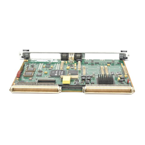
- Page 1 MVME2100 Single Board Computer Programmer’s Reference Guide V2100A/PG2 June 2001 Edition...
- Page 2 Motorola and the Motorola symbol are registered trademarks of Motorola, Inc. PowerPC and the PowerPC logo are registered trademarks; and PowerPC 603e is a trademark of International Business Machines Corporation and are used by Motorola, Inc. under license from International Business Machines Corporation.
- Page 3 The safety precautions listed below represent warnings of certain dangers of which Motorola is aware. You, as the user of the product, should follow these warnings and all other safety precautions necessary for the safe operation of the equipment in your operating environment.
- Page 4 Flammability All Motorola PWBs (printed wiring boards) are manufactured with a flammability rating of 94V-0 by UL-recognized manufacturers. EMI Caution This equipment generates, uses and can radiate electromagnetic energy. It may cause or be susceptible to electromagnetic interference (EMI) if not installed and used with adequate EMI protection.
- Page 5 While reasonable efforts have been made to assure the accuracy of this document, Motorola, Inc. assumes no liability resulting from any omissions in this document, or from the use of the information obtained therein. Motorola reserves the right to revise this document and to make changes from time to time in the content hereof without obligation of Motorola to notify any person of such revision or changes.
- Page 6 If the documentation contained herein is supplied, directly or indirectly, to the U.S. Government, the following notice shall apply unless otherwise agreed to in writing by Motorola, Inc. Use, duplication, or disclosure by the Government is subject to restrictions as set forth in subparagraph (b)(3) of the Rights in Technical Data clause at DFARS 252.227-7013 (Nov.
-
Page 7: Table Of Contents
Contents About This Manual Summary of Changes ....................xiii Overview of Contents ....................xiii Comments and Suggestions ..................xiv Conventions Used in This Manual................xiv Terminology......................xv CHAPTER 1 Product Dataand Memory Maps Introduction........................1-1 What this Guide Provides ...................1-1 Memory maps ......................1-4 Processor Memory Map..................1-4 Address Map A (PReP) ................1-4 Address Map B (CHRP) ................1-6 PCI Memory Map ....................1-7... - Page 8 PCI/PMC Expansion Capability................. 2-5 PCI Configuration Space..................2-5 Memory Characteristics..................... 2-6 System Memory ....................2-6 FLASH Memory....................2-6 APPENDIX A Related Documentation Motorola Computer Group Documents ..............A-1 Manufacturers’ Documents ..................A-2 Related Specifications ....................A-4 MCG Customer Services ..................A-6 viii...
- Page 9 List of Figures Figure 1-1. MVME2100 Block Diagram ..............1-3 Figure 2-1. MVME 2100 PCI Arbitration ..............2-1...
- Page 11 List of Tables Table 1-1. MVME2100 Key Features ................1-2 Table 1-2. Processor Address Map A (PReP) ............1-4 Table 1-3. Processor Address Map B (CHRP)............1-6 Table 1-4. PCI Memory Master View (PReP) ............1-7 Table 1-5. PCI Memory Master View (CHRP)............1-8 Table 1-6. PCI I/O Address Map A (PReP) ...............1-9 Table 1-7.
-
Page 13: Summary Of Changes
MVME2100 Single Board Computer. It provides specific programming information and data applicable to the board. As of the printing date of this manual, the MVME2100 is available in the configurations shown below. -
Page 14: Comments And Suggestions
Chapter 1, Product Data and Memory Maps, provides an overview of the MVME2100 including a table of key features and a block diagram. The remainder of the chapter includes a description of the Memory Maps including Processor Memory Map information, PCI Memory Map information, PCI I/O Memory Map information, and System I/O Memory Map information. -
Page 15: Terminology
bold is used for user input that you type just as it appears; it is also used for commands, options and arguments to commands, and names of programs, directories and files. italic is used for names of variables to which you assign values. Italic is also used for comments in screen displays and examples, and to introduce new terms. - Page 16 In this manual, assertion and negation are used to specify forcing a signal to a particular state. In particular, assertion and assert refer to a signal that is active or true; negation and negate indicate a signal that is inactive or false.
-
Page 17: Introduction
1Product Data and Memory Maps Introduction The MVME2100 is a “state-of-the-art” Single Board Computer. It is based on the MPC8240 Integrated Processor and includes support circuitry such as SDRAM, PROM/Flash memory, and bridge to the VMEbus. Note Unless otherwise specified, the designation “MVME2100” refers to all models of the MVME2100-series Single Board Computers. -
Page 18: Table 1-1. Mvme2100 Key Features
Product Data and Memory Maps The following table lists the key features of the MVME2100. Table 1-1. MVME2100 Key Features Processors • MPC8240 • Bus Clock Frequencies of 66.67 or 83.33 MHz Flash Memory • 1 MB via two 32-pin PLCC/CLCC Sockets for 1MB (8-bit);... - Page 19 Generator 16550 DRAM 32/64MB MPC8240 EEPROM ETHERNET LXT970 DEC21143 PC-MIP TYPE II Slot 2 PC-MIP TYPE II Slot 1 Expansion Connector Slot PC-MIP TYPE I Slot 1 PC-MIP TYPE I Slot 2 Universe II Figure 1-1. MVME2100 Block Diagram http://www.motorola.com/computer/literature...
-
Page 20: Memory Maps
The Processor Memory Map is controlled by the Processor Peripheral device. The MPC8240 supports two address maps designated address Map A (PReP) and address Map B (CHRP). The MVME2100 defaults to address Map A when power is first applied or after a hard reset has occurred. - Page 21 4. Reads to this address generate PCI interrupt-acknowledge cycles. 5. ROM/FLASH bank 1 may contain up to 8MB of 64-bit wide FLASH memory. 6. ROM/FLASH bank 0 may contain up to 1MB of FLASH memory on the MVME2100 and is accessed byte wide. http://www.motorola.com/computer/literature...
-
Page 22: Address Map B (Chrp)
Product Data and Memory Maps Address Map B (CHRP) The system software may initialize the processor to use Address Map B. The following table shows the recommended CHRP Memory Map from the point of view of the Processor. Table 1-3. Processor Address Map B (CHRP) Processor Address Size Definition... -
Page 23: Pci Memory Map
The PCI Memory Map is controlled by the processor peripheral device. The MPC8240 supports two address mapping configurations designated address Map A (PReP), address Map B (CHRP). The MVME2100 defaults to address map A when power is first applied or after a hard reset has occurred. -
Page 24: Pci Memory Map B (Chrp)
2. ROM/FLASH bank 1 may contain up to 8MB of 64-bit wide FLASH memory. 3. ROM/FLASH bank 0 may contain up to 1MB of FLASH memory on the MVME2100 and is accessed byte wide. Computer Group Literature Center Web Site... -
Page 25: Pci I/O Memory Map
The PCI I/O Memory Map is controlled by the processor peripheral device. The MPC8240 supports two address mapping configurations designated address Map A (PReP), address Map B (CHRP). The MVME2100 defaults to address map A when power is first applied or after a hard reset has occurred. -
Page 26: System I/O Memory Map
NVRAM/RTC, and the 16550 UART are mapped into the lower 1MB address range of FLASH/ROM bank 0 (0xFFE00000 - 0xFFEFFFFF). The following table shows the system I/O memory map for the MVME2100. Table 1-8. System I/O Memory Map Address... - Page 27 NVRAM/RTC Notes 1. Recommended function for all MPC8240 based designs. 2. Optional function implemented on the MVME2100. 3. Optional function not implemented on the MVME2100. 4. Only required if more than 512KB of NVRAM is implemented. 5. The MVME2100 implements 8KB of NVRAM.
-
Page 28: System Status Register 1
FIELD OPER RESET RESET Setting this bit will force a hard reset of the MVME2100. This bit will always be cleared during a read. ABORT This bit reflects the current state of the onboard abort signal. This is a debounced version of the abort switch and may be used to determine the state of the abort switch. -
Page 29: System Status Register 2
System I/O Memory Map System Status Register 2 The MVME2100 contains a System Status Register that may be used to generate a hard reset to the board, to control status indicators, and to provide a reference clock for the CPU. The following table provides the necessary information on the System Status Register 2. -
Page 30: Pci Presence Detect Register
Product Data and Memory Maps PCI Presence Detect Register The MVME2100 contains a PCI Presence Detect Register that may be read by the system software to determine the presence of optional PCI devices. The following table provides the necessary information on the PCI Presence Detect Register. -
Page 31: Vmebus Geographical Address Register
The MVME2100 contains a VMEbus Geographical Address register that may be read by the system software to determine the VMEbus board slot that the MVME2100 is plugged into. The following table provides the necessary information on the VMEbus Geographical Address Register. -
Page 32: Configuration Header Register
Product Data and Memory Maps Configuration Header Register The MVME2100 contains an 8-bit user defined header that may be read by the software. The following table provides the necessary information on the Configuration Header Register. Table 1-13. Configuration Header Register... -
Page 33: Simm/Dimm Parallel Presence Detection Registers
SIMM or DIMM memory sockets using a parallel presence detection scheme. Note These registers are not implemented on the MVME2100. Attempts to read these registers will result in indeterminate data being returned. - Page 34 Product Data and Memory Maps 1-18 Computer Group Literature Center Web Site...
-
Page 35: Introduction
2Programming Details Introduction This chapter provides details of several programming functions applicable to the MVME 2100 Single Board Computer. PCI Arbitration PCI arbitration for the MVME 2100 is provided by the integrated PCI arbiter internal to the MPC8240 processor in conjunction with an external sub-arbiter. -
Page 36: Interrupt Handling
Programming Details Interrupt Handling The MVME 2100 uses the Embedded Programmable Interrupt Controller (EPIC) integrated into the processor to manage locally generated interrupts. The interrupt controller will operate in the serial interrupt mode. Currently defined external interrupting devices and serial interrupt assignments are shown in the table below: Table 2-1. -
Page 37: Eeprom Functionality
256 (max) Undefined SDRAM Configuration EEPROM EEPROMs are used on the MVME2100 to contain information regarding the SDRAM devices installed. The data is formatted in accordance to JEDEC standard JESD21-C. The information contained in these EEPROM(s) will be used by the system software to configure the memory controller function integrated into the MPC8240 peripheral device. -
Page 38: Input/Output Functionality
System Configuration EEPROM described earlier. PMC/PC-MIP Type I Expansion Slot As a factory option the MVME2100 may be populated to support either one PCI Mezzanine Card slot or one PC-MIP Type I PCI slot for user-defined functions. -
Page 39: Pci/Pmc Expansion Capability
Input/Output Functionality PCI/PMC Expansion Capability The MVME2100 provides additional PCI/PMC capability through the use of a 114-pin Mictor connector that is compatible with other VMEbus processor boards. By using existing PMCspan carrier boards up to four additional PMC boards can be used. -
Page 40: Memory Characteristics
Programming Details Memory Characteristics System Memory System memory for the MVME2100 is provided by 2 banks of synchronous DRAM. Each bank consists of five 4Mx16 SDRAM devices providing a 32MB bank organized in a 4Mx72 configuration. This design allows memory configurations of 32 or 64MB that can be supported by the MVME2100. -
Page 41: Motorola Computer Group Documents
ARelated Documentation Motorola Computer Group Documents The Motorola publications listed below are referenced in this manual. You can obtain paper or electronic copies of Motorola Computer Group publications by: Contacting your local Motorola sales office Visiting Motorola Computer Group’s World Wide Web literature site, http://www.motorola.com/computer/literature... -
Page 42: Manufacturers' Documents
Table A-2. Manufacturers’ Documents Publication Document Title Number MPC8240 Integrated Processor User’s Manual MPC8240UM/D Motorola Literature Distribution Center Telephone: (800) 441-2447 or (303) 675-2140 MPC8240 White Paper MPC8240WP Motorola Literature Distribution Center Telephone: (800) 441-2447 or (303) 675-2140 MPC8240 Technical Summary... - Page 43 1000 East Bell Road Phoenix, AZ 85022 DIGITAL Semiconductor 21143 EC-QWC4E-TE PCI/CardBus 10/100-Mb/s Ethernet LAN Controller, Hardware Reference Manual Digital Equipment Corp. Maynard, Massachusetts DIGITAL Semiconductor 21143 EC-QWC3C-TE PCI/CardBus 10/100-Mb/s Ethernet LAN Controller Data Sheet Digital Equipment Corp. Maynard, Massachusetts http://www.motorola.com/computer/literature...
-
Page 44: Related Specifications
Related Specifications Related Specifications For additional information, refer to the following table for related specifications. For your convenience, a source for the listed document is also provided. Note In many cases, the information is preliminary and the revision levels of the documents are subject to change without notice. - Page 45 445 Hoes Lane P.O Box 1331 Piscataway, NJ 08855-1331 Common Mezzanine Card Specification P1386 IEEE Standards Department Draft 2.0 445 Hoes Lane P.O Box 1331 Piscataway, NJ 08855-1331 PCI Interface Specification Rev 2.1 PCI Rev 2.1 PCI Special Interest Group 503-696-2000 http://www.motorola.com/computer/literature...
-
Page 46: Mcg Customer Services
MCG Customer Services MCG Customer Services The Motorola Computer Group Customer Services organization provides numerous services to support the needs of our OEM customers throughout the qualification, development, deployment, and continued service phases of their product life cycles. Specific areas of support include:... - Page 47 Glossary Acronyms and Abbreviations The following table explains some of the abbreviations, acronyms, and key terms used in this document Term Meaning ASIC Application Specific Integrated Circuit CHRP (PowerPC) Common Hardware Reference Platform Central Processing Unit DIMM Dual In-line Memory Module Direct Memory Access DRAM Dynamic Random Access Memory...
- Page 48 Glossary Term Meaning Megahertz NVRAM Non-Volatile Random Access Memory Peripheral Component Interconnect PLCC Plastic Leaded Chip Carrier PCI Mezzanine Card (IEEE P1386.1) PReP PowerPC Reference Platform Random Access Memory Read-Only Memory Real-Time Clock Single Board Computer Serial Communication Controller SDRAM Synchronous Dynamic Access Memory SIMM Single In-line Memory Module...
- Page 49 EEPROM device IDs from the MPC8240 Embedded Programmable Interrupt Control- Embedded Programmable Interrupt Control- block diagram ler (EPIC) MVME2100 error notification and handling BORT switch Ethernet Controller Bus Clock Frequencies FLASH Memory CHRP locations, access, device IDs starting PCI Memory address require-...
- Page 50 MPC8240 Technical Summary Configuration Header Register 1-16 MPC8240 Training Manual PCI Presence Detect Register 1-14 MPC8240 White Paper 1-1, SIMM/DIMM Parallel Presence Detec- MVME2100 Block Diagram tion Registers 1-17 MVME2100 SBC VMEbus Geographical Address Register described 1-15 RESET switch ROM/FLASH bank 0 1-5,...
- Page 51 System I/O Memory Map 1-10 System Memory System Status Register 1-13 System Status Register 1 1-12 Universe’s involvement VME SBC MVME2100 described VMEbus Geographical Address bits 1-15 VMEbus Geographical Address Parity 1-15 VMEbus Geographical Address Register 1-15 VMEbus Interface VMEbus interface http://www.motorola.com/computer/literature...
- Page 52 Index IN-4 Computer Group Literature Center Web Site...
Need help?
Do you have a question about the MVME2100 and is the answer not in the manual?
Questions and answers