Motorola MVME6100 Installation And Use Manual
Single-board computer
Hide thumbs
Also See for MVME6100:
- Installation and user manual (90 pages) ,
- Getting started manual (4 pages)
Table of Contents
Advertisement
Quick Links
Advertisement
Table of Contents

Related Manuals for Motorola MVME6100


Summary of Contents for Motorola MVME6100
- Page 1 MVME6100 Single-Board Computer Installation and Use V6100A/IH1 June 2004 Edition...
- Page 2 © Copyright 2004 Motorola Inc. All rights reserved. Printed in the United States of America. Motorola and the stylized M logo are trademarks of Motorola, Inc., registered in the U.S. Patent and Trademark Office. All other product or service names mentioned in this document are the property of their respective owners.
-
Page 3: Safety Summary
Safety Summary The following general safety precautions must be observed during all phases of operation, service, and repair of this equipment. Failure to comply with these precautions or with specific warnings elsewhere in this manual could result in personal injury or damage to the equipment. The safety precautions listed below represent warnings of certain dangers of which Motorola is aware. -
Page 4: Emi Caution
Flammability All Motorola PWBs (printed wiring boards) are manufactured with a flammability rating of 94V-0 by UL-recognized manufacturers. EMI Caution This equipment generates, uses and can radiate electromagnetic energy. It Caution may cause or be susceptible to electromagnetic interference (EMI) if not installed and used with adequate EMI protection. - Page 5 CE Notice (European Community) Warning This is a Class A product. In a domestic environment, this product may cause radio interference, in which case the user may be required to take adequate measures. Warning Motorola Computer Group products with the CE marking comply with the EMC Directive (89/336/EEC).
- Page 6 Notice While reasonable efforts have been made to assure the accuracy of this document, Motorola, Inc. assumes no liability resulting from any omissions in this document, or from the use of the information obtained therein. Motorola reserves the right to revise this document and to make changes from time to time in the content hereof without obligation of Motorola to notify any person of such revision or changes.
-
Page 7: Table Of Contents
SROM Configuration Switch (S3) ..............1-10 Flash Boot Bank Select Configuration Switch (S4) ........1-11 Hardware Installation ..................... 1-12 Installing the MVME6100 into a Chassis ............1-12 Connection to Peripherals ..................1-13 Completing the Installation ..................1-14 CHAPTER 2 Startup and Operation Introduction ...................... - Page 8 MOTLoad Utility Applications ................. 3-2 MOTLoad Tests ....................3-2 Using MOTLoad ....................3-4 Command Line Interface ................... 3-4 Command Line Help ..................3-5 Command Line Rules ..................3-6 MOTLoad Command List ..................3-7 Default VME Settings .................... 3-12 Firmware Settings ....................3-16 CR/CSR Settings .....................
- Page 9 I2C Serial Interface and Devices ............... 4-9 Interrupt Controller ................... 4-9 PCI Bus Arbitration ..................4-10 VMEbus Interface ....................4-11 PMCspan Interface ....................4-11 Flash Memory ......................4-11 System Memory ..................... 4-11 Asynchronous Serial Ports ..................4-11 PCI Mezzanine Card Slots ..................4-12 Real-Time Clock/NVRAM/Watchdog Timer ............
- Page 10 APPENDIX B Thermal Validation Thermally Significant Components ................. B-1 Component Temperature Measurement ..............B-5 Preparation ......................B-5 Measuring Junction Temperature ..............B-5 Measuring Case Temperature ................B-5 Measuring Local Air Temperature ..............B-8 APPENDIX C Related Documentation Motorola Computer Group Documents ..............C-1 Manufacturers’...
- Page 11 List of Figures Figure 1-1. MVME6100 Layout ................1-7 Figure 4-1. MVME6100 Block Diagram ..............4-3 Figure B-1. Thermally Significant Components—Primary Side ......B-3 Figure B-2. Thermally Significant Components—Secondary Side ......B-4 Figure B-3. Mounting a Thermocouple Under a Heatsink ........B-7 Figure B-4. Measuring Local Air Temperature ............B-8...
- Page 12 List of Tables Table 1-1. Startup Overview ..................1-3 Table 1-2. MVME6100 Jumper and Switch Settings ..........1-6 Table 1-3. SROM Configuration Switch (S3) ............1-10 Table 1-4. Configuration Switch (S4) ..............1-12 Table 1-5. MVME6100 Connectors ..............1-14 Table 2-1. Front-Panel LED Status Indicators ............2-2 Table 3-1.
- Page 13 Table A-2. MVME6100 Specifications ..............A-2 Table B-1. Thermally Significant Components ............B-2 Table C-1. Motorola Computer Group Documents ..........C-1 Table C-2. Manufacturers’ Documents ..............C-2 Table C-3. Related Specifications ................C-5...
-
Page 14: About This Manual
MVME6100 single-board computer. It provides specific preparation and installation information, and data applicable to the board. As of the printing date of this manual, the MVME6100 supports the models listed below. Model Number... -
Page 15: Overview Of Contents
Chapter 3, MOTLoad Firmware, describes the basic features of the MOTLoad firmware product. Chapter 4, Functional Description, describes the MVME6100 on a block diagram level. Chapter 5, Pin Assignments, provides pin assignments for various headers and connectors on the MMVE6100 single-board computer. -
Page 16: Comments And Suggestions
Comments and Suggestions Motorola welcomes and appreciates your comments on its documentation. We want to know what you think about our manuals and how we can make them better. Mail comments to: Motorola Computer Group Reader Comments DW164 2900 S. Diablo Way Tempe, Arizona 85282 You can also submit comments to the following e-mail address: reader-comments@mcg.mot.com... - Page 17 <Enter>, <Return> or <CR> represents the carriage return or Enter key. Ctrl represents the Control key. Execute control characters by pressing the Ctrl key and the letter simultaneously, for example, Ctrl-d. xviii...
-
Page 18: Introduction
46 from J24 of PMC slot 2 are routed to row D and row Z of P2. The MVME6100 has two planar PCI buses (PCI0 and PCI1). In order to support a more generic PCI bus hierarchy nomenclature, the MV64360 PCI buses will be referred to in this document as PCI bus 0 (root bridge instance 0, bus 0) and PCI bus 1 (root bridge instance 1, bus 0). - Page 19 VIO, either +3.3V or +5V. The MVME6100 board interfaces to the VMEbus via the P1 and P2 connectors, which use 5-row 160-pin connectors as specified in the VME64 Extension Standard. It also draws +12V and +5V power from the VMEbus backplane through these two connectors.
-
Page 20: Getting Started
MVME5500 and is accomplished by configuring the on-board jumpers. Getting Started This section provides an overview of the steps necessary to install and power up the MVME6100 and a brief section on unpacking and ESD precautions. Overview of Startup Procedures... -
Page 21: Unpacking Guidelines
Hardware Preparation and Installation Unpacking Guidelines Unpack the equipment from the shipping carton. Refer to the packing list and verify that all items are present. Save the packing material for storing and reshipping of equipment. Note If the shipping carton is damaged upon receipt, request that the carrier’s agent be present during the unpacking and inspection of the equipment. -
Page 22: Hardware Configuration
To produce the desired configuration and ensure proper operation of the MVME6100, you may need to carry out certain hardware modifications before installing the module. Most options on the MVME6100 are software configurable. Configuration changes are made by setting bits in control registers after the board is installed in a system. -
Page 23: Table 1-2. Mvme6100 Jumper And Switch Settings
Write Protect A, Write Protect B, Boot Bank Select, and Safe Start Note Items in brackets are factory default settings. The MVME6100 is factory tested and shipped with the configuration described in the following sections. Computer Group Literature Center Web Site... -
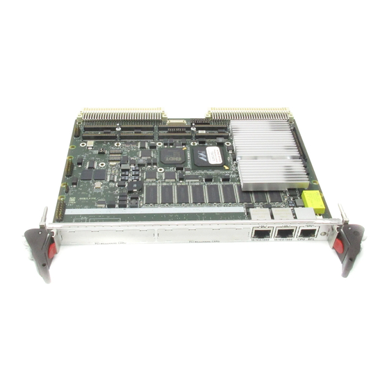
Page 24: Figure 1-1. Mvme6100 Layout
MVME6100 Preparation IPMC ABT/RST 4296 0604 Figure 1-1. MVME6100 Layout http://www.motorola.com/computer/literature... -
Page 25: Scon Header (J7)
Hardware Preparation and Installation SCON Header (J7) A 3-pin planar header allows the choice for auto/enable/disable SCON VME configuration. A jumper installed across pins 1 and 2 configures for SCON always enabled. A jumper installed across pins 2 and 3 configures for SCON disabled. -
Page 26: Front/Rear Ethernet And Transition Module Options Header (J30)
Front/Rear Ethernet and Transition Module Options Header (J30) IPMC P2 I/O for IPMC Mode (factory configuration) PMC1 P2 I/O for PMC Mode Front/Rear Ethernet and Transition Module Options Header (J30) A 40-pin planar header allows for selecting P2 options. Jumpers installed across Row A pins 3-10 and Row B pins 3-10 enable front Ethernet access. -
Page 27: Srom Configuration Switch (S3)
Hardware Preparation and Installation The following illustration shows jumper setting options for J30. The factory default is shown where applicable: J30 Options Front Ethernet Rear Ethernet Non-Specific Transition Module (Default) (Default) PMC I/O TO P2 MVME 712M MVME 761 (Default) Transition Module Transition Module 4294 0604... -
Page 28: Flash Boot Bank Select Configuration Switch (S4)
Flash Boot Bank Select Configuration Switch (S4) S3 position 3-8 defines the VME Geographical Address if the MVME6100 is installed in a 3-row backplane. The following is the pinout: Position Function VMEGAP_L VMEGA4_L VMEGA3_L VMEGA2_L VMEGA1_L VMEGA0_L Setting the individual position to ON forces the corresponding signal to zero. -
Page 29: Hardware Installation
4295 0604 Hardware Installation Installing the MVME6100 into a Chassis Use the following steps to install the MVME6100 into your computer chassis. 1. Attach an ESD strap to your wrist. Attach the other end of the ESD strap to an electrical ground (refer to Unpacking Guidelines). -
Page 30: Connection To Peripherals
2. Remove any filler panel that might fill that slot. 3. Install the top and bottom edge of the MVME6100 into the guides of the chassis. Warning Only use injector handles for board insertion to avoid damage/deformation to the front panel and/or PCB. -
Page 31: Completing The Installation
Table 1-5 lists them for you. Refer to Chapter 5, Pin Assignments for the pin assignments of the connectors listed below. Table 1-5. MVME6100 Connectors Connector Function IPMC761/712 connector PMC expansion connector J9, J93... -
Page 32: Introduction
Tsi148 VME Bridge ASIC, PCI6520, PMC1/2 slots, both Ethernet PHYs, serial ports, PMCspan slot, both flash banks, and the device bus control PLD. If the MVME6100 is enabled for VME system controller, the VME bus will be reset and local reset input is sent to the Tsi148 VME controller. -
Page 33: Table 2-1. Front-Panel Led Status Indicators
Startup and Operation The MVME6100 has two front-panel indicators: BDFAIL, software controlled and asserted by firmware (or other software) to indicate a configuration problem (or other failure) CPU, connected to a CPU bus control signal to indicate bus transfer activity The following table describes these indicators: Table 2-1. -
Page 34: Introduction
MOTLoad Implementation and Memory Requirements The implementation of MOTLoad and its memory requirements are product specific. The MVME6100 single-board computer (SBC) is offered with a wide range of memory (for example, DRAM, external cache, flash). Typically, the smallest amount of on-board DRAM that a Motorola SBC... -
Page 35: Motload Commands
MOTLoad Firmware has is 32MB. Each supported Motorola product line has its own unique MOTLoad binary image(s). Currently the largest MOTLoad compressed image is less than 1MB in size. MOTLoad Commands MOTLoad supports two types of commands (applications): utilities and tests. - Page 36 MOTLoad Tests All MOTLoad tests are designed to validate functionality with minimum user interaction. Once launched, most MOTLoad tests operate automatically without any user interaction. There are a few tests where the functionality being validated requires user interaction (that is, switch tests, interactive plug-in hardware modules, etc.).
-
Page 37: Using Motload
MOTLoad then performs the specified action. An example of a MOTLoad command line prompt is shown below. The MOTLoad prompt changes according to what product it is used on (for example, MVME5500, MVME6100). Example: MVME6100>... -
Page 38: Command Line Help
Command Line Help Example: MVME6100> version Copyright: Motorola Inc.1999-2002, All Rights Reserved MOTLoad RTOS Version 2.0 PAL Version 0.1 (Motorola MVME6100) Example: MVME6100> ver Copyright: Motorola Inc. 1999-2002, All Rights Reserved MOTLoad RTOS Version 2.0 PAL Version 0.1 (Motorola MVME6100) -
Page 39: Command Line Rules
Option arguments immediately follow (no spaces) the option All commands, command options, and device tree strings are case sensitive Example: MVME6100> flashProgram –d/dev/flash0 –n00100000 For more information on MOTLoad operation and function, refer to the MOTLoad Firmware Package User’s Manual. Computer Group Literature Center Web Site... -
Page 40: Motload Command List
MOTLoad Command List MOTLoad Command List The following table provides a list of all current MOTLoad commands. Products supported by MOTLoad may or may not employ the full command set. Typing help at the MOTLoad command prompt will display all commands supported by MOTLoad for a given product. Table 3-1. - Page 41 MOTLoad Firmware Table 3-1. MOTLoad Commands (continued) Command Description diskBoot Disk Boot (Direct-Access Mass-Storage Device) downLoad Down Load S-Record from Host One-Line Instruction Disassembler echo Echo a Line of Text elfLoader ELF Object File Loader errorDisplay Display the Contents of the Test Error Status Table eval Evaluate Expression execProgram...
- Page 42 MOTLoad Command List Table 3-1. MOTLoad Commands (continued) Command Description help Display Command/Test Help Strings l2CacheShow Display state of L2 Cache and L2CR register contents l3CacheShow Display state of L3 Cache and L3CR register contents mdb mdh mdw Memory Display Bytes/Halfwords/Words memShow Display Memory Allocation mmb mmh mmw...
- Page 43 MOTLoad Firmware Table 3-1. MOTLoad Commands (continued) Command Description Symbol Table Attach Symbol Table Lookup stop Stop Date and Time (Power-Save Mode) taskActive Display the Contents of the Active Task Table Trace (Single-Step) User Program Trace (Single-Step) User Program to Address testDisk Test Disk testEnetPtP...
- Page 44 MOTLoad Command List Table 3-1. MOTLoad Commands (continued) Command Description testRtcTick RTC Tick testSerialExtLoop Serial External Loopback testSeriallntLoop Serial Internal Loopback testStatus Display the Contents of the Test Status Table testSuite Execute Test Suite testSuiteMake Make (Create) Test Suite testThermoOp Thermometer Temp Limit Operational Test testThermoQ Thermometer Temp Limit Quick Test...
-
Page 45: Default Vme Settings
MOTLoad Firmware Default VME Settings As shipped from the factory, the MVME6100 has the following VME configuration programmed via Global Environment Variables (GEVs) for the Tsi148 VME controller. The firmware allows certain VME settings to be changed in order for the user to customize the environment. The following is a description of the default VME settings that are changeable by the user. - Page 46 CRG Base Address Lower Register = 00000000 MVME6100> The CRG Attribute Register is set to the default (RESET) condition. MVME6100> vmeCfg –s –i0 Displaying the selected Default VME Setting - interpreted as follows: Inbound Image 0 Attribute Register = 000227AF...
- Page 47 0x70000000, thus an access to 0x91000000 on the PCI-X Local Bus becomes an access to 0x01000000 on the VMEbus. MVME6100> vmeCfg –s –o2 Displaying the selected Default VME Setting - interpreted as follows: Outbound Image 2 Attribute Register = 80001061...
- Page 48 0x4C000000, thus an access to 0xB3FF0000 on the PCI-X Local Bus becomes an access to 0xFFFF0000 on the VMEbus. MVME6100> vmeCfg –s –o7 Displaying the selected Default VME Setting - interpreted as follows: Outbound Image 7 Attribute Register = 80001065...
-
Page 49: Firmware Settings
Firmware Settings The following sections provide additional information pertaining to the VME firmware settings of the MVME6100. A few VME settings are controlled by hardware jumpers while the majority of the VME settings are managed by the firmware command utility vmeCfg. -
Page 50: Editing Vme Settings
Editing VME Settings vmeCfg –s –r404 Displays Miscellaneous Control Register state vmeCfg –s –r40C Displays User AM Codes Register state vmeCfg –s –rF70 Displays VMEbus Register Access Image Control Register state Editing VME Settings To edit the changeable VME setting, type the following at the firmware prompt: vmeCfg –e –m Edits Master Enable state... -
Page 51: Deleting Vme Settings
MOTLoad Firmware Deleting VME Settings To delete the changeable VME setting (restore default value), type the following at the firmware prompt: vmeCfg –d –m Deletes Master Enable state vmeCfg –d –i(0 - 7) Deletes selected Inbound Window state vmeCfg –d –o(0 - 7) Deletes selected Outbound Window state vmeCfg –d –r184 Deletes PCI Miscellaneous Register state... -
Page 52: Remote Start
For further details on CR/CSR space, please refer to the VME64 Specification, listed in Appendix C, Related Documentation. The MVME6100 uses a Discovery II for its VME bridge. The offsets of the mailboxes in the Discovery II are defined in the Discovery II User Manual, http://www.motorola.com/computer/literature 3-19... -
Page 53: Alternate Boot Images And Safe Start
The MVME6100’s IBCA needs to be mapped appropriately through the master’s VMEbus bridge. For example, to use remote start using mailbox 0 on an MVME6100 installed in slot 5, the master would need a mapping to support reads and writes of address 0x002ff348 in VME CR/CSR space (0x280000 + 0x7f348). -
Page 54: Firmware Scan For Boot Image
Firmware Scan for Boot Image Search the active flash bank, possibly interactively, for a valid POST image. If found, the POST images executes. Once completed, the POST image returns and startup continues. Search the active flash bank, possibly interactively, for a valid USER boot image. - Page 55 MOTLoad Firmware Address Usage 0xFFF00000 to 0xFFFFFFFF Boot block. Recovery code 0xFFE00000 to 0XFFFFFFFF Reserved for MCG use. (MOTLoad update image) 0xFFD00000 to 0xFFDFFFFF First possible alternate image (FBD00000 or F7D00000) (Bank B / Bank A actual) 0xFFC00000 to 0xFFCFFFFF Second possible alternate image (FBC00000 or F7C00000) (Bank B / Bank A actual)
-
Page 56: Valid Boot Images
NOPQRSTUVabcdefghijk#lmn3opqrsstuvxyzaWXZ Copyright Motorola Inc. 1999-2004, All Rights Reserved MOTLoad RTOS Version 2.0, PAL Version 0.b EA02 MVME6100> Valid Boot Images Valid boot images whether POST, USER, or MCG, are located on 1MB boundaries within flash. The image may exceed 1MB in size. An image is determined valid through the presence of two "valid image keys"... -
Page 57: Checksum Algorithm
MOTLoad Firmware Checksum Algorithm The checksum algorithm is a simple unsigned word add of each word (4 byte) location in the image. The image must be a multiple of 4 bytes in length (word-aligned). The content of the checksum location in the header is not part of the checksum calculation. -
Page 58: User Images
USER Images COPY_TO_RAM If set, this flag indicates that the image is to be copied to RAM at the address specified in the header before control is passed. If not set, the image will be executed in Flash. In both instances, control will be passed at the image offset specified in the header from the base of the image. -
Page 59: Alternate Boot Data Structure
/* board's RAM size in MB */ void flashPtr; /* ptr to this image in flash */ char boardType[16]; /* name string, eg MVME6100 */ void globalData; /* 16K, zeroed, user defined */ unsigned int reserved[12]; } altBootData_t;... - Page 60 Alternate Boot Data Structure state that the board was in at POST entry. USER images should not return control to the boot loader. http://www.motorola.com/computer/literature 3-27...
-
Page 61: Features
4Functional Description This chapter describes the MVME6100 on a block diagram level. Features The following table lists the features of the MVME6100. Table 4-1. MVME6100 Features Summary Feature Description Processor – Single 1.267 GHz MPC7457 processor – Bus clock frequency at 133 MHz –... - Page 62 Functional Description Table 4-1. MVME6100 Features Summary (continued) Feature Description NVRAM – 32KB provided by MK48T37 with SnapHat battery backup Real-Time Clock Watchdog Timer On-board Peripheral – Dual 10/100/1000 Ethernet ports routed to front panel RJ-45 Support connectors, one optionally routed to P2 backplane –...
-
Page 63: Block Diagram
4250 0604 Figure 4-1. MVME6100 Block Diagram Processor The MVME6100 supports the MPC7457 with adjustable core voltage supply. The maximum external processor bus speed is 133 MHz. The processor core frequency runs at 1.267 GHz or the highest speed MPC7457 can support, which is determined by the processor core voltage, the external speed, and the internal VCO frequency. -
Page 64: L3 Cache
Functional Description L3 Cache The MVME6100 external L3 cache is implemented using two 8Mb DDR SRAM devices. The L3 cache bus is 72-bits wide (64 bits of data and 8 bits of parity) and operates at 211 MHz. The L3 cache interface is implemented with an on-chip, 8-way, set-associative tag memory. -
Page 65: Cpu Bus Interface
Documentation, for additional information and programming details. Memory Controller Interface The MVME6100 supports two banks of DDR SDRAM using 256Mb/ 512Mb DDR SDRAM devices on-board. 1Gb DDR non-stacked SDRAM devices may be used when available. 133 MHz operation should be used for all memory options. -
Page 66: Device Controller Interface
Flash Banks A and B, NVRAM/RTC. Each bank supports up to 512MB of address space, resulting in total device space of 1.5GB. Serial ports are the fourth and fifth devices on the MVME6100. Each bank has its own parameters register as shown in the following table. -
Page 67: Gigabit Ethernet Macs
CPU bus or the PCI buses. Gigabit Ethernet MACs The MVME6100 supports two 10/100/1000Mb/s full duplex Ethernet ports connected to the front panel via the MV64360 system controller. Ethernet access is provided by front panel RJ-45 connectors with integrated magnetics and LEDs. -
Page 68: General-Purpose Timers/Counters
Documentation, for additional information and programming details. O Message Unit O compliant messaging for the MVME6100 board is provided by an I messaging unit integrated into the MV64360 system controller. The MV64360 messaging unit includes hardware hooks for message transfers between PCI devices and the CPU. -
Page 69: I2C Serial Interface And Devices
Appendix C, Related Documentation, for additional information and programming details. C Serial Interface and Devices A two-wire serial interface for the MVME6100 board is provided by a master/slave capable I C serial controller integrated into the MV64360 device. The I C serial controller provides two basic functions. -
Page 70: Pci Bus Arbitration
(the MPP pins function as general-purpose inputs). Software configures the MPP pins to function as request/grant pairs for the internal PCI arbiter. The arbitration pairs for the MVME6100 are assigned to the MPP pins as shown in the MVME6100 Programmer’s Guide. -
Page 71: Vmebus Interface
VME64x (VITA 1.5) compatible backplanes, such as 5-row backplanes, to achieve maximum VMEbus performance. PMCspan Interface The MVME6100 provides a PCI expansion connector to add more PMC interfaces than the two on the MVME6100 board. The PMCspan interface is provided through the PCI6520 PCIx/PCIx bridge. -
Page 72: Pci Mezzanine Card Slots
115 Kbaud. PCI Mezzanine Card Slots The MVME6100 board supports two PMC slots. Two sets of four EIA- E700 AAAB connectors are located on the MVME6100 board to interface to the 32-bit/64-bit IEEE P1386.1 PMC to add any desirable function. The PMC slots are PCI/PCI-X 33/66/100 capable. -
Page 73: Real-Time Clock/Nvram/Watchdog Timer
62.5 msec (1/16s) and maximum time-out period is 124 seconds. The interface for the Timekeeper and SRAM is connected to the MV64360 device controller bus on the MVME6100 board. Refer to the MV64360 Data Sheet, listed in Appendix C, Related Documentation, for additional information and programming details. -
Page 74: Idsel Routing
PCI agent to an A/D signal as defined in version 2.2 of the PCI specification. IDSEL assignments to on-board resources are specified in the MVME6100 Programmer’s Guide. Reset Control Logic The sources of reset on the MVME6100 are the following: Powerup Reset Switch NVRAM Watchdog Timer MV64360 Watchdog Timer VMEbus controller –... -
Page 75: Introduction
5Pin Assignments Introduction This chapter provides pin assignments for various headers and connectors on the MMVE6100 single-board computer. PMC Expansion Connector (J4) Gigabit Ethernet Connectors (J9, J93) PCI Mezzanine Card (PMC) Connectors (J11 – J14, J21 – J24) COM1 Connector (J19) VMEbus P1 Connector VMEbus P2 Connector (IPMC Mode) The following headers are described in this chapter:... -
Page 76: Table 5-1. Pmc Expansion Connector (J4) Pin Assignments
Pin Assignments Table 5-1. PMC Expansion Connector (J4) Pin Assignments Signal Signal +3.3V +3.3V PCICLK PMCINTA# PMCINTB# PURST# PMCINTC# HRESET# PMCINTD# TRST# PCIXP# PCIXGNT# PCIXREQ# +12V -12V PERR# SERR# LOCK# SDONE DEVSEL# SBO# TRDY# IRDY# STOP# FRAME# M66EN ACK64# Reserved REQ64# Reserved Computer Group Literature Center Web Site... - Page 77 PMC Expansion Connector (J4) Table 5-1. PMC Expansion Connector (J4) Pin Assignments (continued) Signal Signal PCIRST# C/BE1# C/BE0# C/BE3# C/BE2# AD11 AD10 AD13 AD12 AD15 AD14 AD17 AD16 AD19 AD18 AD21 AD20 AD23 AD22 AD25 AD24 AD27 AD26 AD29 AD28 AD31 AD30 http://www.motorola.com/computer/literature...
- Page 78 Pin Assignments Table 5-1. PMC Expansion Connector (J4) Pin Assignments (continued) Signal Signal PAR64 Reserved C/BE5# C/BE4# C/BE7# C/BE6# AD33 AD32 AD35 AD34 AD37 AD36 AD39 AD38 AD41 AD40 AD43 AD42 AD45 AD44 AD47 AD46 AD49 AD48 AD51 AD50 AD53 AD52 AD55 AD54...
-
Page 79: Gigabit Ethernet Connectors (J9, J93)
Access to the dual Gigabit Ethernet is provided by two transpower RJ-45 connectors with integrated magnetics and LEDs located on the front panel of the MVME6100. The pin assignments for these connectors are as follows: Table 5-2. Gigabit Ethernet Connectors (J9, J93) -
Page 80: Table 5-3. Pmc Slot 1 Connector (J11) Pin Assignments
Pin Assignments PCI Mezzanine Card (PMC) Connectors (J11 – J14, J21 – J24) There are eight 64-pin SMT connectors on the MVME6100 to provide 32/64-bit PCI interfaces and P2 I/O for two optional add-on PMCs. Note PMC slot connectors J14 and J24 contain the signals that go to VME P2 I/O rows A, C, D, and Z. -
Page 81: Pci Mezzanine Card (Pmc) Connectors (J11 - J14, J21 - J24)
PCI Mezzanine Card (PMC) Connectors (J11 – J14, J21 – J24) Table 5-3. PMC Slot 1 Connector (J11) Pin Assignments (continued) Signal Signal DEVSEL# LOCK# PCI_RSVD PCI_RSVD +3.3V (VIO) AD15 AD12 AD11 AD09 C/BE0# AD06 AD05 AD04 +3.3V (VIO) AD03 AD02 AD01 AD00... - Page 82 Pin Assignments Table 5-4. PMC Slot 1 Connector (J12) Pin Assignments (continued) Signal Signal +3.3V Pull-down Not Used AD30 AD29 AD26 AD24 +3.3V IDSEL1 AD23 +3.3V AD20 AD18 AD16 C/BE2# IDSEL1B TRDY# +3.3V STOP# PERR# +3.3V SERR# C/BE1# AD14 AD13 M66EN AD10 AD08...
-
Page 83: Table 5-5. Pmc Slot 1 Connector (J13) Pin Assignments
PCI Mezzanine Card (PMC) Connectors (J11 – J14, J21 – J24) Table 5-5. PMC Slot 1 Connector (J13) Pin Assignments Signal Signal Reserved C/BE7# C/BE6# C/BE5# C/BE4# +3.3V (VIO) PAR64 AD63 AD62 AD61 AD60 AD59 AD58 AD57 +3.3V (VIO) AD56 AD55 AD54 AD53... -
Page 84: Table 5-6. Pmc Slot 1 Connector (J14) Pin Assignments
Pin Assignments Table 5-5. PMC Slot 1 Connector (J13) Pin Assignments (continued) Signal Signal AD36 AD35 AD34 AD33 +3.3V (VIO) AD32 Reserved Reserved Reserved Reserved Table 5-6. PMC Slot 1 Connector (J14) Pin Assignments Signal Signal PMC0_1 (P2-C1) PMC0_2 (P2-A1) PMC0_3 (P2-C2) PMC0_4 (P2-A2) PMC0_5 (P2-C3) - Page 85 PCI Mezzanine Card (PMC) Connectors (J11 – J14, J21 – J24) Table 5-6. PMC Slot 1 Connector (J14) Pin Assignments (continued) Signal Signal PMC0_29 (P2-C15) PMC0_30 (P2-A15) PMC0_31 (P2-C16) PMC0_32 (P2-A16) PMC0_33 (P2-C17) PMC0_34 (P2-A17) PMC0_35 (P2-C18) PMC0_36 (P2-A18) PMC0_37 (P2-C19) PMC0_38 (P2-A19) PMC0_39 (P2-C20) PMC0_40 (P2-A20)
-
Page 86: Table 5-7. Pmc Slot 2 Connector (J21) Pin Assignments
Pin Assignments Table 5-7. PMC Slot 2 Connector (J21) Pin Assignments Signal Signal -12V INTC# INTD# INTA# PMCPRSNT1# INTB# PCI_RSVD +3.3Vaux PMCGNT1# PMCREQ1# +3.3V (VIO) AD31 AD28 AD27 AD25 C/BE3# AD22 AD21 AD19 +3.3V (VIO) AD17 FRAME# IRDY# DEVSEL# LOCK# PCI_RSVD PCI_RSVD +3.3V (VIO) -
Page 87: Table 5-8. Pmc Slot 2 Connector (J22) Pin Assignments
PCI Mezzanine Card (PMC) Connectors (J11 – J14, J21 – J24) Table 5-7. PMC Slot 2 Connector (J21) Pin Assignments (continued) Signal Signal C/BE0# AD06 AD05 AD04 +3.3V (VIO) AD03 AD02 AD01 AD00 REQ64# Table 5-8. PMC Slot 2 Connector (J22) Pin Assignments Signal Signal... - Page 88 Pin Assignments Table 5-8. PMC Slot 2 Connector (J22) Pin Assignments (continued) Signal Signal AD18 AD16 C/BE2# IDSEL1B TRDY# +3.3V STOP# PERR# +3.3V SERR# C/BE1# AD14 AD13 M66EN AD10 AD08 +3.3V AD07 REQ1B# +3.3V GNT1B# Not Used Not Used EREADY1 Not Used ACK64# +3.3V...
-
Page 89: Table 5-9. Pmc Slot 2 Connector (J23) Pin Assignments
PCI Mezzanine Card (PMC) Connectors (J11 – J14, J21 – J24) Table 5-9. PMC Slot 2 Connector (J23) Pin Assignments Signal Signal Reserved C/BE7# C/BE6# C/BE5# C/BE4# +3.3V (VIO) PAR64 AD63 AD62 AD61 AD60 AD59 AD58 AD57 +3.3V (VIO) AD56 AD55 AD54 AD53... -
Page 90: Table 5-10. Pmc Slot 2 Connector (J24) Pin Assignments
Pin Assignments Table 5-9. PMC Slot 2 Connector (J23) Pin Assignments (continued) Signal Signal AD36 AD35 AD34 AD33 +3.3V (VIO) AD32 Reserved Reserved Reserved Reserved Table 5-10. PMC Slot 2 Connector (J24) Pin Assignments Signal Signal PMC1_1 (P2-D1) PMC1_2 (P2-Z1) PMC1_3 (P2-D2) PMC1_4 (P2-D3) PMC1_5 (P2-Z3) - Page 91 PCI Mezzanine Card (PMC) Connectors (J11 – J14, J21 – J24) Table 5-10. PMC Slot 2 Connector (J24) Pin Assignments (continued) Signal Signal PMC1_29 (P2-Z19) PMC1_30 (P2-D20) PMC1_31 (P2-D21) PMC1_32 (P2-Z21) PMC1_33 (P2-D22 PMC1_34 (P2-D23) PMC1_35 (P2-Z23) PMC1_36 (P2-D24) PMC1_37 (P2-D25) PMC1_38 (P2-Z25 PMC1_39 (P2-D26) PMC1_40 (P2-D27)
-
Page 92: Com1 Connector (J19)
Pin Assignments COM1 Connector (J19) A standard RJ-45 connector located on the front panel of the MVME6100 provides the interface to the asynchronous serial debug port. The pin assignments for this connector are as follows: Table 5-11. COM1 Connector (J19) Pin Assignments... - Page 93 VMEbus P1 Connector Table 5-12. VMEbus P1 Connector Pin Assignments (continued) ROW Z ROW A ROW B ROW C ROW D BG1IN* Reserved Reserved BG1OUT* Reserved BG2IN* Reserved Reserved BG2OUT* Reserved SYSCLK BG3IN* SYSFAIL* Reserved Reserved BG3OUT* BERR* Reserved DS1* BR0* SYSRESET* Reserved...
-
Page 94: Vmebus P2 Connector (Pmc Mode)
VMEBus P2 Connector (PMC Mode) The VME P2 connector is an 160-pin DIN. Row B of the P2 connector provides power to the MVME6100 and to the upper eight VMEbus address lines and additional 16 VMEbus data lines. The pin assignments for the P2 connector are as follows: Table 5-13. - Page 95 VMEBus P2 Connector (PMC Mode) Table 5-13. VMEbus P2 Connector Pin Assignments (PMC Mode) (continued) ROW Z ROW A ROW B ROW C ROW D PMC0_16 VA28 PMC0_15 PMC1_12 (J14-16) (J14-15) (J24-12) PMC1_14 PMC0_18 VA29 PMC0_17 PMC1_13 (J24-14) (J14-18) (J14-17) (J24-13) PMC0_20 VA30...
- Page 96 Pin Assignments Table 5-13. VMEbus P2 Connector Pin Assignments (PMC Mode) (continued) ROW Z ROW A ROW B ROW C ROW D PMC1_35 PMC0_46 VD24 PMC0_45 PMC1_34 (J24-35) (J14-46) (J24-34) (J14-45) PMC0_48 VD25 PMC0_47 PMC1_36 (J14-48) (J14-47) (J24-36) P2_IO_GLAN1_ PMC0_50 VD26 PMC0_49 PMC1_37...
-
Page 97: Vmebus P2 Connector (Ipmc Mode)
VMEbus P2 Connector (IPMC Mode) The VME P2 connector is an 160-pin DIN. Row B of the P2 connector provides power to the MVME6100 and to the upper eight VMEbus address lines and additional 16 VMEbus data lines. The pin assignments for the P2 connector are as follows: Table 5-14. -
Page 98: Table 5-15. Vme P2 Connector Pinouts With Ipmc761
Pin Assignments Table 5-14. VME P2 Connector Pinouts with IPMC712 (continued) Row Z Row A Row B Row C Row D PMC2_32 (J24-32) RTS3 VD23 P IME PMC2_31 (J24-31) CTS3 P FAULT# PMC2_33 (J24-33) PMC2_35 (J24-35) DTR3 VD24 TXD1_232 PMC2_34 (J24-34) DCD3 VD25 RXD1... - Page 99 VMEbus P2 Connector (IPMC Mode) Table 5-15. VME P2 Connector Pinouts with IPMC761 (continued) Row Z Row A Row B Row C Row D DB13# BSY# VA31 PRD2 PMC2_16 (J24-16) ACK# PRD3 PMC2_18 (J24-18) DB14# RST# PRD4 PMC2_19 (J24-19) MSG# VD16 PRD5 PMC2_21 (J24-21)
-
Page 100: Headers
Note Rows A and C and Zs (Z1, 3, 5, 7, 9, 11, 13, 15, and 17) functionality is provided by the IPMC761 in slot 1 and the MVME6100 Ethernet port 2. Headers SCON Header (J7) A 3-pin planar header allows the choice for auto/enable/disable SCON VME configuration. -
Page 101: Boundary Scan Header (J8)
Boundary Scan Header (J8) Boundary Scan Header (J8) The 14-pin boundary scan header provides an interface for programming the on-board PLDs and for boundary scan testing/debug purposes. The pin assignments for this header are as follows: Table 5-17. Boundary Scan Header (J8) Pin Assignments Signal Signal TRST_L... -
Page 102: Com2 Header (J29)
Pin Assignments Table 5-18. PMC/IPMC Configuration Jumper Block Pin/Row 1 Pin/Row 2 Pin/Row 3 (PMC I/O) (P2 Pins) (IPMC Pins) PMC1_IO(17) P2_PMC1_IO(17) IPMC DB13_L PMC1_IO(20) P2_PMC1_IO(20) IPMC DB14_L PMC1_IO(23) P2_PMC1_IO(23) IPMC DB15_L PMC1_IO(26) P2_PMC1_IO(26) IPMC DBP1_L A jumper installed across pins 2 and 3 on all nine headers selects PMC1 I/O for IPMC mode. -
Page 103: Front/Rear Ethernet And Transition Module Options Header (J30)
Front/Rear Ethernet and Transition Module Options Header (J30) Front/Rear Ethernet and Transition Module Options Header (J30) The pin assignments for this connector are as follows: Table 5-20. Front/Rear Ethernet and Transition Module Options Header (J30) Pin Assignment Row D Row B Row A (From PMC Row C... -
Page 104: Processor Jtag/Cop Header (J42)
Pin Assignments Processor JTAG/COP Header (J42) There is one standard 16-pin header that provides an interface for the RISCWatch function. The pin assignments for this header are as follows: Table 5-21. Processor JTAG/COP (RISCWatch) Header (J42) Pin Assignments Signal Signal CPU_TDO CPU_QACK_L CPU_TDI... -
Page 105: Power Requirements
ASpecifications Power Requirements In its standard configuration, the MVME6100 requires +5V, +12V, and –12V for operation. On-board converters supply the processor core voltage, +3.3V, +1.8V, and +2.5V. Supply Current Requirements Table A-1 provides an estimate of the typical and maximum current required from each of the input supply voltages. -
Page 106: Environmental Specifications
Specifications Environmental Specifications Table A-2 lists the environmental specifications, along with the board dimensions. Table A-2. MVME6100 Specifications Characteristics Specifications Operating Temperature 0° to +55° C or 32° to 131° F (forced air cooling required) 400 LFM (linear feet per minute) of forced air cooling is recommended for operation in the upper temperature range. -
Page 107: Thermally Significant Components
BThermal Validation Board component temperatures are affected by ambient temperature, air flow, board electrical operation, and software operation. In order to evaluate the thermal performance of a circuit board assembly, it is necessary to test the board under actual operating conditions. These operating conditions vary depending on system design. -
Page 108: Table B-1. Thermally Significant Components
Thermal Validation refers to the temperature at the top, center surface of the component. Air temperature refers to the ambient temperature near the component. Table B-1. Thermally Significant Components Max. Allowable Component Reference Temperature Measurement Designator Generic Description (deg. C) Location U3-U11, DDR SDRAM... -
Page 109: Figure B-1. Thermally Significant Components-Primary Side
Thermally Significant Components IPMC ABT/RST 4248 0504 Figure B-1. Thermally Significant Components—Primary Side http://www.motorola.com/computer/literature... -
Page 110: Figure B-2. Thermally Significant Components-Secondary Side
Thermal Validation 4292 0504 Figure B-2. Thermally Significant Components—Secondary Side Computer Group Literature Center Web Site... -
Page 111: Component Temperature Measurement
Component Temperature Measurement Component Temperature Measurement The following sections outline general temperature measurement methods. For the specific types of measurements required for thermal evaluation of this board, see Table B-1. Preparation We recommend 40 AWG (American wire gauge) thermocouples for all thermal measurements. - Page 112 Thermal Validation Note Machining a heatsink base reduces the contact area between the heatsink and the electrical component. You can partially compensate for this effect by filling the machined areas with thermal grease. The grease should not contact the thermocouple junction.
-
Page 113: Figure B-3. Mounting A Thermocouple Under A Heatsink
Measuring Case Temperature Machined groove for thermocouple wire routing Thermocouple junction bonded to component ISOMETRIC VIEW Machined groove for Through hole for thermocouple thermocouple wire junction clearance (may require routing removal of fin material) Also use for alignment guidance during heatsink installation Thermal pad Heatsink base HEATSINK BOTTOM VIEW... -
Page 114: Measuring Local Air Temperature
Thermal Validation Measuring Local Air Temperature Measure local component ambient temperature by placing the thermocouple downstream of the component. This method is conservative since it includes heating of the air by the component. The following figure illustrates one method of mounting the thermocouple. Tape thermocouple wire to top of component Thermocouple... -
Page 115: Motorola Computer Group Documents
Visiting Motorola Computer Group’s World Wide Web literature site, http://www.motorola.com/computer/literature Table C-1. Motorola Computer Group Documents Motorola Publication Document Title Number MVME6100 Single-Board Computer Programmer’s V6100A/PG Reference Guide MOTLoad Firmware Package User’s Manual MOTLODA/UM IPMC712/761 I/O Module Installation and Use VIPMCA/IH... -
Page 116: Manufacturers' Documents
Related Documentation Manufacturers’ Documents For additional information, refer to the following table for manufacturers’ data sheets or user’s manuals. As an additional help, a source for the listed document is provided. Please note that, while these sources have been verified, the information is subject to change without notice. Table C-2. - Page 117 Manufacturers’ Documents Table C-2. Manufacturers’ Documents (continued) Document Title and Source Publication Number BCM5421S 10/100/1000BASE-T Gigabit Transceiver with SERDES 5421S-DS05-D2 Interface 10/25/02 Broadcom Corporation Web Site: http://www.broadcom.com 3 Volt Intel StrataFlash Memory 290737 28F256K3 Intel Corporation Literature Center 19521 E. 32nd Parkway Aurora CO 80011-8141 Web Site: http://developer.intel.com/design/flcomp/datashts/290737.htm...
- Page 118 Related Documentation Table C-2. Manufacturers’ Documents (continued) Document Title and Source Publication Number 3.3V-5V 256Kbit (32Kx8) Timekeeper SRAM M48T37V ST Microelectronics 1000 East Bell Road Phoenix, AZ 85022 Web Site: http://www.st.com/stonline/books/toc/index.htm 2-Wire Serial CMOS EEPROM AT24C02N AT24C64A Atmel Corporation San Jose, CA Web Site: http://www.atmel.com/atmel/support/ Dallas Semiconductor DS1621Digital Thermometer and Thermostat...
-
Page 119: Related Specifications
Related Specifications Related Specifications For additional information, refer to the following table for related specifications. For your convenience, a source for the listed document is also provided. It is important to note that in many cases, the information is preliminary and the revision levels of the documents are subject to change without notice. - Page 120 Index display VME settings 3-16 documentation, related abort/reset switch air temperature range ambient temperature, measuring edit VME settings 3-17 ambient temperatures environmental specifications applying power ESD precautions evaluating thermal performance block diagram board features, hardware component temperatures firmware command utility 3-16 connectors 1-13...
- Page 121 processor jumper settings related documentation relative humidity L3 cache LEDs remote start 3-19 board fail restore VME settings 3-18 CPU bus activity settings, VME 3-12 list of commands specifications MOTLoad startup overview suggestions, submitting xvii manual conventions xvii switch, abort/reset manufacturers’...
Need help?
Do you have a question about the MVME6100 and is the answer not in the manual?
Questions and answers