Motorola MVME6100 Installation And User Manual
Hide thumbs
Also See for MVME6100:
- Installation and use manual (121 pages) ,
- Getting started manual (4 pages)
Table of Contents
Advertisement
Quick Links
Advertisement
Table of Contents

Related Manuals for Motorola MVME6100


Summary of Contents for Motorola MVME6100
- Page 1 MVME6100 Single-Board Computer Installation and Use V6100A/IH2 April 2006 Edition...
- Page 2 Printed in the United States of America. Trademarks Motorola and the stylized M logo are trademarks registered in the U.S. Patent and Trademark Office. All other product or service names mentioned in this document are the property of their respective holders.
- Page 3 The safety precautions listed below represent warnings of certain dangers of which Motorola is aware. You, as the user of the product, should follow these warnings and all other safety precautions necessary for the safe operation of the equipment in your operating environment.
- Page 4 Flammability All Motorola PWBs (printed wiring boards) are manufactured with a flammability rating of 94V-0 by UL- recognized manufacturers. EMI Caution This equipment generates, uses and can radiate electromagnetic energy. It may cause Caution or be susceptible to electromagnetic interference (EMI) if not installed and used with adequate EMI protection.
- Page 5 Motorola reserves the right to revise this document and to make changes from time to time in the content hereof without obligation of Motorola to notify any person of such revision or changes.
-
Page 6: Table Of Contents
Installing the MVME6100 into a Chassis ........ - Page 7 PCI Mezzanine Card Slots ............43 viii MVME6100 Installation and Use (V6100A/IH2)
- Page 8 Related Documentation ............77 Motorola Embedded Communications Computing Documents ......77 Manufacturers’...
- Page 9 Figure 4-1. MVME6100 Block Diagram ........
- Page 10 Table 1-2. MVME6100 Jumper and Switch Settings ........
-
Page 11: About This Manual
MVME6100 single-board computer. It provides specific preparation and installation information, and data applicable to the board. As of the printing date of this manual, the MVME6100 supports the models listed below. Model Number... -
Page 12: Conventions Used In This Manual
(for example, screen displays, reports), examples, and system prompts. <Enter>, <Return> or <CR> represents the carriage return or Enter key. Ctrl represents the Control key. Execute control characters by pressing the Ctrl key and the letter simultaneously, for example, Ctrl-d. MVME6100 Installation and Use (V6100A/IH2) -
Page 13: Hardware Preparation And Installation
2 are routed to row D and row Z of P2. The MVME6100 has two planar PCI buses (PCI0 and PCI1). In order to support a more generic PCI bus hierarchy nomenclature, the MV64360 PCI buses will be referred to in this document as PCI bus 0 (root bridge instance 0, bus 0) and PCI bus 1 (root bridge instance 1, bus 0). -
Page 14: Getting Started
Discovery II PHB (MV64360) does not recognize address lines below AD16. For this reason, although an IPMC7xx module may be used on an MVME6100, the serial and parallel ports are not available, nor addressable. This issue will be resolved by MCG at a later date. -
Page 15: Overview Of Startup Procedures
Avoid touching areas of integrated circuitry; static discharge can damage circuits. Caution Caution Motorola strongly recommends that you use an antistatic wrist strap and a conductive Use ESD foam pad when installing or upgrading a system. Electronic components, such as disk drives, computer boards, and memory modules can be extremely sensitive to electrostatic discharge (ESD). -
Page 16: Hardware Configuration
This section discusses certain hardware and software tasks that may need to be performed prior to installing the board in a chassis. To produce the desired configuration and ensure proper operation of the MVME6100, you may need to carry out certain hardware modifications before installing the module. -
Page 17: Table 1-2. Mvme6100 Jumper And Switch Settings
Chapter 1 Hardware Preparation and Installation Table 1-2. MVME6100 Jumper and Switch Settings Jumper/ Switch Function Settings SCON Header [No jumper installed] Auto-SCON Always SCON No SCON J10, PMC/IPMC Selection Headers [Jumper installed] J15–J18, PMC I/O J25–J28 [2-3] IPMC I/O for IPMC7xx... -
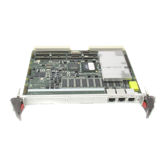
Page 18: Figure 1-1. Mvme6100 Layout
Chapter 1 Hardware Preparation and Installation The MVME6100 is factory tested and shipped with the configuration described in the following sections. Figure 1-1. MVME6100 Layout IPMC ABT/RST 4296 0604 MVME6100 Installation and Use (V6100A/IH2) -
Page 19: Scon Header (J7)
A jumper installed across pins 1 and 2 on all nine headers selects PMC1 for PMC I/O mode. A jumper across pins 2 and 3 on all nine headers selects IPMC I/O mode. IPMC P2 I/O for IPMC Mode (factory configuration) PMC1 P2 I/O for PMC Mode MVME6100 Installation and Use (V6100A/IH2) -
Page 20: Front/Rear Ethernet And Transition Module Options Header (J30)
The SROM WP switch is OFF to enable write protection on all I C. The switch is ON to disable the I C EEPROM write protection. Table 1-3. SROM Configuration Switch (S3) POSITION FUNCTION SROM WP SROM_INIT DEFAULT (OFF) No SROM_INIT MVME6100 Installation and Use (V6100A/IH2) -
Page 21: Flash Boot Bank Select Configuration Switch (S4)
Chapter 1 Hardware Preparation and Installation S3 position 3-8 defines the VME Geographical Address if the MVME6100 is installed in a 3-row backplane. The following is the pinout: Positio Function VMEGAP_L VMEGA4_L VMEGA3_L VMEGA2_L VMEGA1_L VMEGA0_L Setting the individual position to ON forces the corresponding signal to zero. If the board is installed in a 5-row backplane, the geographical address is defined by the backplane and positions 3-8 of S3 should be set to OFF. -
Page 22: Hardware Installation
Slide the MVME6100 into the chassis until resistance is felt. Simultaneously move the injector/ejector levers in an inward direction. Verify that the MVME6100 is properly seated and secure it to the chassis using the two screws located adjacent to the injector/ejector levers. -
Page 23: Connection To Peripherals
Chapter 1 Hardware Preparation and Installation Connection to Peripherals When the MVME6100 is installed in a chassis, you are ready to connect peripherals and apply power to the board. Figure 1-1 on page 6 shows the locations of the various connectors while... -
Page 24: Startup And Operation
Bridge ASIC, PCI6520, PMC1/2 slots, both Ethernet PHYs, serial ports, PMCspan slot, both flash banks, and the device bus control PLD. If the MVME6100 is enabled for VME system controller, the VME bus will be reset and local reset input is sent to the Tsi148 VME controller. -
Page 25: Motload Firmware
The implementation of MOTLoad and its memory requirements are product specific. The MVME6100 single-board computer (SBC) is offered with a wide range of memory (for example, DRAM, external cache, flash). Typically, the smallest amount of on-board DRAM that a Motorola SBC has is 32MB. -
Page 26: Motload Utility Applications
All testSuites that are included as part of a product specific MOTLoad firmware package are product specific. For more information, refer to the testSuite command description page in the MOTLoad Firmware Package User’s Manual. MVME6100 Installation and Use (V6100A/IH2) -
Page 27: Using Motload
MOTLoad is an ever changing firmware package, so user-input shortcuts may change as command additions are made. Example: MVME6100> version Copyright: Motorola Inc.1999-2002, All Rights Reserved MOTLoad RTOS Version 2.0 PAL Version 0.1 (Motorola MVME6100) Example: MVME6100>... -
Page 28: Command Line Help
Chapter 3 MOTLoad Firmware Copyright: Motorola Inc. 1999-2002, All Rights Reserved MOTLoad RTOS Version 2.0 PAL Version 0.1 (Motorola MVME6100) If the partial command string cannot be resolved to a single unique command, MOTLoad will inform the user that the command was ambiguous. -
Page 29: Motload Command List
ISO9660 File System File Load clear Clear the Specified Status/History Table(s) Turns on Concurrent Mode csb csh csw Calculates a Checksum Specified by Command-line Options devShow Display (Show) Device/Node Table diskBoot Disk Boot (Direct-Access Mass-Storage Device) MVME6100 Installation and Use (V6100A/IH2) - Page 30 Display Memory Allocation mmb mmh mmw Memory Modify Bytes/Halfwords/Words netBoot Network Boot (BOOT/TFTP) netShow Display Network Interface Configuration Data netShut Disable (Shutdown) Network Interface netStats Display Network Interface Statistics Data noCm Turns off Concurrent Mode MVME6100 Installation and Use (V6100A/IH2)
- Page 31 RAM Addressing testRamAlt RAM Alternating testRamBitToggle RAM Bit Toggle testRamBounce RAM Bounce testRamCodeCopy RAM Code Copy and Execute testRamEccMonitor Monitor for ECC Errors testRamMarch RAM March testRamPatterns RAM Patterns testRamPerm RAM Permutations testRamQuick RAM Quick MVME6100 Installation and Use (V6100A/IH2)
- Page 32 Display Task Status upLoad Up Load Binary Data from Target version Display Version String(s) vmeCfg Manages user specified VME configuration parameters vpdDisplay VPD Display vpdEdit VPD Edit waitProbe Wait for I/O Probe to Complete MVME6100 Installation and Use (V6100A/IH2)
-
Page 33: Default Vme Settings
Chapter 3 MOTLoad Firmware Default VME Settings As shipped from the factory, the MVME6100 has the following VME configuration programmed via Global Environment Variables (GEVs) for the Tsi148 VME controller. The firmware allows certain VME settings to be changed in order for the user to customize the environment. The following is a description of the default VME settings that are changeable by the user. - Page 34 Displaying the selected Default VME Setting - interpreted as follows: Outbound Image 3 Attribute Register = 80001061 Outbound Image 3 Starting Address Upper Register = 00000000 Outbound Image 3 Starting Address Lower Register = B3FF0000 MVME6100 Installation and Use (V6100A/IH2)
-
Page 35: Firmware Settings
Firmware Settings The following sections provide additional information pertaining to the VME firmware settings of the MVME6100. A few VME settings are controlled by hardware jumpers while the majority of the VME settings are managed by the firmware command utility vmeCfg. -
Page 36: Editing Vme Settings
Edits Special PCI Target Image Register state ■ vmeCfg –e –r400 Edits Master Control Register state ■ vmeCfg –e –r404 Edits Miscellaneous Control Register state ■ vmeCfg –e –r40C Edits User AM Codes Register state MVME6100 Installation and Use (V6100A/IH2) -
Page 37: Deleting Vme Settings
These transactions occur across the VMEbus in the case of the MVME6100. MOTLoad uses one of four mailboxes in the Tsi148 VME controller as the inter-board communication address (IBCA) between the host and the target. - Page 38 For further details on CR/CSR space, please refer to the VME64 Specification, listed in Appendix C, Related Documentation. The MVME6100 uses a Discovery II for its VME bridge. The offsets of the mailboxes in the Discovery II are defined in the Discovery II User Manual, listed in Appendix C, Related...
-
Page 39: Alternate Boot Images And Safe Start
Some later versions of MOTLoad support Alternate Boot Images and a Safe Start recovery procedure. If Safe Start is available on the MVME6100, Alternate Boot Images are supported. With Alternate Boot Image support, the bootloader code in the boot block examines the upper 8MB of the flash bank for Alternate Boot images. - Page 40 Addr FFE00000 Size 00100000 Flags 00000003 Name: MOTLoad Addr FFD00000 Size 00100000 Flags 00000003 Name: MOTLoad boot> c NOPQRSTUVabcdefghijk#lmn3opqrsstuvxyzaWXZ Copyright Motorola Inc. 1999-2004, All Rights Reserved MOTLoad RTOS Version 2.0, PAL Version 0.b EA02 MVME6100> MVME6100 Installation and Use (V6100A/IH2)
-
Page 41: Valid Boot Images
The algorithm is implemented using the following code: Unsigned int checksum( Unsigned int *startPtr,/* starting address */ Unsigned int endPtr/* ending address */ unsigned int checksum=0; while (startPtr < endPtr) { checksum += *startPtr; startPtr++; return(checksum); MVME6100 Installation and Use (V6100A/IH2) -
Page 42: Motload Image Flags
The MMU is disabled. ■ L1 instruction cache has been initialized and is enabled. ■ L1 data cache has been initialized (invalidated) and is disabled. ■ L2 cache is disabled. ■ L3 cache is disabled. MVME6100 Installation and Use (V6100A/IH2) -
Page 43: Alternate Boot Data Structure
{ unsigned int ramSize;/* board’s RAM size in MB */ void flashPtr;/* ptr to this image in flash */ char boardType[16];/* name string, eg MVME6100 */ void globalData;/* 16K, zeroed, user defined */ unsigned int reserved[12]; } altBootData_t;... -
Page 44: Functional Description
Functional Description This chapter describes the MVME6100 on a block diagram level. Features The following table lists the features of the MVME6100. Table 4-1. MVME6100 Features Summary Feature Description Processor – Single 1.267 GHz MPC7457 processor – Bus clock frequency at 133 MHz –... -
Page 45: Block Diagram
Chapter 4 Functional Description Table 4-1. MVME6100 Features Summary (continued) Feature Description VME Interface – Tsi148 VME 2eSST ASIC provides: ■ Eight programmable VMEbus map decoders ■ A16, A24, A32, and A64 address ■ 8-bit, 16-bit, and 32-bit single cycle data transfers ■... -
Page 46: Processor
L3 Cache The MVME6100 external L3 cache is implemented using two 8Mb DDR SRAM devices. The L3 cache bus is 72-bits wide (64 bits of data and 8 bits of parity) and operates at 211 MHz. The L3 cache interface is implemented with an on-chip, 8-way, set-associative tag memory. -
Page 47: Cpu Bus Interface
Documentation, for additional information and programming details. Memory Controller Interface The MVME6100 supports two banks of DDR SDRAM using 256Mb/ 512Mb DDR SDRAM devices on-board. 1Gb DDR non-stacked SDRAM devices may be used when available. 133 MHz operation should be used for all memory options. The SDRAM supports ECC and the MV64360 supports single-bit and double-bit error detection and single-bit error correction of all SDRAM reads and writes. -
Page 48: Device Controller Interface
Banks A and B, NVRAM/RTC. Each bank supports up to 512MB of address space, resulting in total device space of 1.5GB. Serial ports are the fourth and fifth devices on the MVME6100. Each bank has its own parameters register as shown in the following table. -
Page 49: Sram
Documentation, for additional information and programming details. C Serial Interface and Devices A two-wire serial interface for the MVME6100 board is provided by a master/slave capable I serial controller integrated into the MV64360 device. The I C serial controller provides two basic functions. -
Page 50: Interrupt Controller
The MVME6100 uses the interrupt controller integrated into the MV64360 device to manage the MV64360 internal interrupts as well as the external interrupt requests. The interrupts are routed to the MV64360 MPP pins from on-board resources as shown in the MVME6100 Programmer’s Guide. The external interrupt sources include the following: ■... -
Page 51: Pci Bus Arbitration
VME64x (VITA 1.5) compatible backplanes, such as 5-row backplanes, to achieve maximum VMEbus performance. PMCspan Interface The MVME6100 provides a PCI expansion connector to add more PMC interfaces than the two on the MVME6100 board. The PMCspan interface is provided through the PCI6520 PCIx/PCIx bridge. -
Page 52: Pci Mezzanine Card Slots
The MVME6100 board supports two PMC slots. Two sets of four EIA-E700 AAAB connectors are located on the MVME6100 board to interface to the 32-bit/64-bit IEEE P1386.1 PMC to add any desirable function. The PMC slots are PCI/PCI-X 33/66/100 capable. -
Page 53: Real-Time Clock/Nvram/Watchdog Timer
62.5 msec (1/16s) and maximum time-out period is 124 seconds. The interface for the Timekeeper and SRAM is connected to the MV64360 device controller bus on the MVME6100 board. Refer to the MV64360 Data Sheet, listed in Appendix C, Related Documentation, for additional information and programming details. -
Page 54: Pin Assignments
SCON Header (J7) ■ Boundary Scan Header (J8) ■ PMC/IPMC Selection Headers (J10, J15 – J18, J25 – J28) ■ COM2 Header (J29) ■ Front/Rear Ethernet and Transition Module Options Header (J30) ■ Processor JTAG/COP Header (J42) MVME6100 Installation and Use (V6100A/IH2) -
Page 55: Connectors
Table 5-1. PMC Expansion Connector (J4) Pin Assignments Signal Signal +3.3V +3.3V PCICLK PMCINTA# PMCINTB# PURST# PMCINTC# HRESET# PMCINTD# TRST# PCIXP# PCIXGNT# PCIXREQ# +12V -12V PERR# SERR# LOCK# SDONE DEVSEL# SBO# TRDY# IRDY# STOP# FRAME# M66EN ACK64# Reserved REQ64# Reserved MVME6100 Installation and Use (V6100A/IH2) - Page 56 Table 5-1. PMC Expansion Connector (J4) Pin Assignments (continued) Signal Signal PCIRST# C/BE1# C/BE0# C/BE3# C/BE2# AD11 AD10 AD13 AD12 AD15 AD14 AD17 AD16 AD19 AD18 AD21 AD20 AD23 AD22 AD25 AD24 AD27 AD26 AD29 AD28 AD31 AD30 MVME6100 Installation and Use (V6100A/IH2)
-
Page 57: Gigabit Ethernet Connectors (J9, J93)
Gigabit Ethernet Connectors (J9, J93) Access to the dual Gigabit Ethernet is provided by two transpower RJ-45 connectors with integrated magnetics and LEDs located on the front panel of the MVME6100. The pin assignments for these connectors are as follows: Table 5-2. -
Page 58: Pci Mezzanine Card (Pmc) Connectors (J11 - J14, J21 - J24)
2. DS1 and DS2 signals are controlled by the on-board Reset PLD. PCI Mezzanine Card (PMC) Connectors (J11 – J14, J21 – J24) There are eight 64-pin SMT connectors on the MVME6100 to provide 32/64-bit PCI interfaces and P2 I/O for two optional add-on PMCs. -
Page 59: Table 5-4. Pmc Slot 1 Connector (J12) Pin Assignments
+3.3V (VIO) AD03 AD02 AD01 AD00 REQ64# Table 5-4. PMC Slot 1 Connector (J12) Pin Assignments Signal Signal +12V TRST# Not Used Not Used Not Used Pull-up +3.3V RST# Pull-down +3.3V Pull-down Not Used AD30 AD29 MVME6100 Installation and Use (V6100A/IH2) -
Page 60: Table 5-5. Pmc Slot 1 Connector (J13) Pin Assignments
Not Used EREADY0 Not Used ACK64# +3.3V No Connect (MONARCH#) Table 5-5. PMC Slot 1 Connector (J13) Pin Assignments Signal Signal Reserved C/BE7# C/BE6# C/BE5# C/BE4# +3.3V (VIO) PAR64 AD63 AD62 AD61 AD60 AD59 AD58 AD57 MVME6100 Installation and Use (V6100A/IH2) -
Page 61: Table 5-6. Pmc Slot 1 Connector (J14) Pin Assignments
PMC0_4 (P2-A2) PMC0_5 (P2-C3) PMC0_6 (P2-A3) PMC0_7 (P2-C4) PMC0_8 (P2-A4) PMC1 _9 (P2-C5) PMC0_10 (P2-A5) PMC0_11 (P2-C6) PMC0_12 (P2-A6) PMC0_13 (P2-C7) PMC0_14 (P2-A7) PMC0_15 (P2-C8) PMC0_16 (P2-A8) PMC0_17 (P2-C9) PMC0_18 (P2-A9) PMC0_19 (P2-C10) PMC0_20 (P2-A10) MVME6100 Installation and Use (V6100A/IH2) -
Page 62: Table 5-7. Pmc Slot 2 Connector (J21) Pin Assignments
PMC0_59 (P2-C30) PMC0_60 (P2-A30) PMC0_61 (P2-C31) PMC0_62 (P2-A31) PMC0_63 (P2-C32) PMC0_64 (P2-A32) Table 5-7. PMC Slot 2 Connector (J21) Pin Assignments Signal Signal -12V INTC# INTD# INTA# PMCPRSNT1# INTB# PCI_RSVD +3.3Vaux PMCGNT1# PMCREQ1# +3.3V (VIO) AD31 MVME6100 Installation and Use (V6100A/IH2) -
Page 63: Table 5-8. Pmc Slot 2 Connector (J22) Pin Assignments
+3.3V (VIO) AD03 AD02 AD01 AD00 REQ64# Table 5-8. PMC Slot 2 Connector (J22) Pin Assignments Signal Signal +12V TRST# Not Used Not Used Not Used Pull-up +3.3V RST# Pull-down +3.3V Pull-down Not Used AD30 AD29 MVME6100 Installation and Use (V6100A/IH2) -
Page 64: Table 5-9. Pmc Slot 2 Connector (J23) Pin Assignments
Not Used EREADY1 Not Used ACK64# +3.3V No Connect (MONARCH#) Table 5-9. PMC Slot 2 Connector (J23) Pin Assignments Signal Signal Reserved C/BE7# C/BE6# C/BE5# C/BE4# +3.3V (VIO) PAR64 AD63 AD62 AD61 AD60 AD59 AD58 AD57 MVME6100 Installation and Use (V6100A/IH2) -
Page 65: Table 5-10. Pmc Slot 2 Connector (J24) Pin Assignments
PMC1_3 (P2-D2) PMC1_4 (P2-D3) PMC1_5 (P2-Z3) PMC1_6 (P2-D4) PMC1_7 (P2-D5) PMC1_8 (P2-Z5) PMC1_9 (P2-D6) PMC1_10 (P2-D7) PMC1_11 (P2-Z7) PMC1_12 (P2-D8) PMC1_13 (P2-D9) PMC1_14 (P2-Z9) PMC1_15 (P2-D10 PMC1_16 (P2-D11) PMC1_17 (P2-Z11) PMC1_18 (P2-D12) PMC1_19 (P2-D13) PMC1_20 (P2-Z13) MVME6100 Installation and Use (V6100A/IH2) -
Page 66: Com1 Connector (J19)
Not Used COM1 Connector (J19) A standard RJ-45 connector located on the front panel of the MVME6100 provides the interface to the asynchronous serial debug port. The pin assignments for this connector are as follows: Table 5-11. COM1 Connector (J19) Pin Assignments... -
Page 67: Vmebus P1 Connector
DS1* BR0* SYSRESET* Reserved Reserved DS0* BR1* LWORD* Reserved WRITE* BR2* Reserved Reserved BR3* Reserved DTACK* Reserved Reserved Reserved Reserved Reserved Reserved IACK* Reserved Reserved IACKIN* SERA Reserved IACKOUT* SERB Reserved Reserved Reserved IRQ7* Reserved MVME6100 Installation and Use (V6100A/IH2) -
Page 68: Vmebus P2 Connector (Pmc Mode)
The VME P2 connector is an 160-pin DIN. Row B of the P2 connector provides power to the MVME6100 and to the upper eight VMEbus address lines and additional 16 VMEbus data lines. The pin assignments for the P2 connector are as follows: Table 5-13. - Page 69 (J14-53)/TXB (J24-40) PMC0_56 VD29 PMC0_55 PMC1_42 (J14-56) (J14-55)/RXB (J24-42) P2_IO_GLAN1_M PMC0_58 VD30 PMC0_57 PMC1_43 DIO_3+ (J14-58) (J14-57)/RTSB (J24-43) PMC0_60 VD31 PMC0_59 PMC1_45 (J14-60) (J14-59)/CTSB (J24-45) P2_IO_GLAN1_M PMC0_62 PMC0_61 DIO_3- (J14-62) (J14-61) PMC0_64 PMC0_63 (J14-64) (J14-63) MVME6100 Installation and Use (V6100A/IH2)
-
Page 70: Vmebus P2 Connector (Ipmc Mode)
The VME P2 connector is an 160-pin DIN. Row B of the P2 connector provides power to the MVME6100 and to the upper eight VMEbus address lines and additional 16 VMEbus data lines. The pin assignments for the P2 connector are as follows: Table 5-14. -
Page 71: Table 5-15. Vme P2 Connector Pinouts With Ipmc761
PMC2_32 TXD3 VD23 INIT# PMC2_31 (J24-31) (J24-32) RXD3 PRFLT# PMC2_33 (J24-33) PMC2_35 RTXC3 VD24 TXD1_232 PMC2_34 (J24-34) (J24-35) TRXC3 VD25 RXD1_232 PMC2_36 (J24-36) PMC2_38 TXD4 VD26 RTS1_232 PMC2_37 (J24-37) (J24-38) RXD4 VD27 CTS1_232 PMC2_39 (J24-39) MVME6100 Installation and Use (V6100A/IH2) -
Page 72: Headers
MCLK Note Rows A and C and Zs (Z1, 3, 5, 7, 9, 11, 13, 15, and 17) functionality is provided by the IPMC761 in slot 1 and the MVME6100 Ethernet port 2. Headers SCON Header (J7) A 3-pin planar header allows the choice for auto/enable/disable SCON VME configuration. A jumper installed across pins 1 and 2 configures for SCON always enabled. -
Page 73: Boundary Scan Header (J8)
IPMC DB12_L PMC1_IO(17) P2_PMC1_IO(17) IPMC DB13_L PMC1_IO(20) P2_PMC1_IO(20) IPMC DB14_L PMC1_IO(23) P2_PMC1_IO(23) IPMC DB15_L PMC1_IO(26) P2_PMC1_IO(26) IPMC DBP1_L A jumper installed across pins 2 and 3 on all nine headers selects PMC1 I/O for IPMC mode. MVME6100 Installation and Use (V6100A/IH2) -
Page 74: Com2 Header (J29)
PMC0_IO(1) P2_C1(P2_IO_GLAN1_M magnetic T2-19 MDI_1N (J9-5) DIO_1-) PMC1_IO(38) P2_Z25(P2_IO_GLAN1_ magnetic T2-17 MDI_2P (J9-6) MDIO_2+) PMC1_IO(41) P2_Z27(P2_IO_GLAN1_ magnetic T2-16 MDI_2N (J9-7) MDIO_2-) PMC1_IO(44) P2_Z29(P2_IO_GLAN1_ magnetic T2-14 MDI_3P (J9-8) MDIO_3+) PMC1_IO(46) P2_Z31(P2_IO_GLAN1_ magnetic T2-13 MDI_3N (J9-9) MDIO_3-) MVME6100 Installation and Use (V6100A/IH2) -
Page 75: Processor Jtag/Cop Header (J42)
Table 5-21. Processor JTAG/COP (RISCWatch) Header (J42) Pin Assignments Signal Signal CPU_TDO CPU_QACK_L CPU_TDI CPU_TRST_L CPU_QREQ_L PU CPU_VIO CPU_TCK OPT PU CPU_VIO CPU_TMS CPU_SRST_L OPTPD_GND CPU_HRST_L KEY (no pin) CPU_CKSTPO_L Note Some signals are actually resistor buffered versions of the named signal. MVME6100 Installation and Use (V6100A/IH2) -
Page 76: Specifications
Specifications Power Requirements In its standard configuration, the MVME6100 requires +5V, +12V, and –12V for operation. On-board converters supply the processor core voltage, +3.3V, +1.8V, and +2.5V. Supply Current Requirements Table A-1 provides an estimate of the typical and maximum current required from each of the input supply voltages. - Page 77 Appendix A Specifications Table A-2. MVME6100 Specifications (continued) Characteristics Specifications Relative Humidity Operating: 5% to 90% non-condensing Non-operating: 5% to 90% non-condensing Vibration Non-operating: 1 G sine sweep, 5–100 Hz, horizontal and vertical (NEBS1) Physical Dimensions 6U, 4HP wide (233 mm x 160 mm x 20 mm) (9.2 in.
-
Page 78: Thermal Validation
These operating conditions vary depending on system design. While Motorola performs thermal analysis in a representative system to verify operation within specified ranges, refer to Appendix A, Specifications, you should evaluate the thermal performance of the board in your application. -
Page 79: Table B-1. Thermally Significant Components
U84, U95 Gigabit Ethernet Transceiver Case U82, U83 Cache Case U45, U46 Programmable Logic Device PCI Bridge Discovery II Case Clock Generator U14, U22 Clock Buffer MC7457RX, 1.267 GHz Processor Case Tsi148 VME Bridge ASIC MVME6100 Installation and Use (V6100A/IH2) -
Page 80: Figure B-1. Thermally Significant Components-Primary Side
Appendix B Thermal Validation Figure B-1. Thermally Significant Components—Primary Side IPMC ABT/RST 4248 0504 MVME6100 Installation and Use (V6100A/IH2) -
Page 81: Figure B-2. Thermally Significant Components-Secondary Side
Appendix B Thermal Validation Figure B-2. Thermally Significant Components—Secondary Side MVME6100 Installation and Use (V6100A/IH2) -
Page 82: Component Temperature Measurement
Make sure that the thermocouple junction contacts only the electrical component. Also make sure that heatsinks lay flat on electrical components. The following figure shows one method of machining a heatsink base to provide a thermocouple routing path. MVME6100 Installation and Use (V6100A/IH2) -
Page 83: Figure B-3. Mounting A Thermocouple Under A Heatsink
ISOMETRIC VIEW Machined groove for Through hole for thermocouple thermocouple wire junction clearance (may require routing removal of fin material) Also use for alignment guidance during heatsink installation Thermal pad Heatsink base HEATSINK BOTTOM VIEW MVME6100 Installation and Use (V6100A/IH2) -
Page 84: Measuring Local Air Temperature
This method is conservative since it includes heating of the air by the component. The following figure illustrates one method of mounting the thermocouple. Figure B-4. Measuring Local Air Temperature Tape thermocouple wire to top of component Thermocouple junction Air flow MVME6100 Installation and Use (V6100A/IH2) -
Page 85: Related Documentation
Related Documentation Motorola Embedded Communications Computing Documents The Motorola publications listed below are referenced in this manual. You can obtain electronic copies of Motorola Embedded Communications Computing (ECC) publications by: ■ Contacting your local Motorola sales office ■ Visiting Motorola ECC’s World Wide Web literature site, http://www.motorola.com/computer/literature... -
Page 86: Manufacturers' Documents
Literature Center 19521 E. 32nd Parkway Aurora CO 80011-8141 Web Site: http://developer.intel.com/design/flcomp/datashts/290737.htm PCI6520 (HB7) Transparent PCIx/PCIx Bridge Preliminary Data Book PCI6520 PLX Technology, Inc. Ver. 0.992 870 Maude Avenue Sunnyvale, California 94085 Web Site: http://www.hintcorp.com/products/hint/default.asp MVME6100 Installation and Use (V6100A/IH2) -
Page 87: Related Specifications
VME64 Specification ANSI/VITA 1-1994 VME64 Extensions ANSI/VITA 1.1-1997 2eSST Source Synchronous Transfer VITA 1.5-199x PCI Special Interest Group (PCI SIG) http://www.pcisig.com/ Peripheral Component Interconnect (PCI) Local Bus Specification, PCI Local Bus Revision 2.0, 2.1, 2.2 Specification MVME6100 Installation and Use (V6100A/IH2) - Page 88 IEEE http://standards.ieee.org/catalog/ IEEE - Common Mezzanine Card Specification (CMC) Institute of P1386 Draft 2.0 Electrical and Electronics Engineers, Inc. IEEE - PCI Mezzanine Card Specification (PMC) P1386.1 Draft 2.0 Institute of Electrical and Electronics Engineers, Inc. MVME6100 Installation and Use (V6100A/IH2)
- Page 89 MOTLoad ESD precautions command characteristics evaluating thermal performance command line help command line rules command types features, hardware command versus test firmware command utility described Flash memory how employed interface list of commands MVME6100 Installation and Use (V6100A/IH2)
- Page 90 VME settings vibration VME settings delete settings, VME display specifications edit startup overview restore suggestions, submitting vmeCfg MVME6100 Installation and Use (V6100A/IH2)
Need help?
Do you have a question about the MVME6100 and is the answer not in the manual?
Questions and answers