Table of Contents
Advertisement
Quick Links
Advertisement
Table of Contents

Related Manuals for Motorola MVME167 Series


Summary of Contents for Motorola MVME167 Series
- Page 1 MVME167 Single Board Computer Installation Guide MVME167IG/D4...
- Page 2 Motorola, Inc. assumes no liability resulting from any omissions in this document, or from the use of the information obtained therein. Motorola reserves the right to revise this document and to make changes from time to time in the content hereof without obligation of Motorola to notify any person of such revision or changes.
- Page 3 Preface This manual provides a general board level hardware description, hardware preparation and installation instructions, debugger general information, and information on using the debugger. This manual applies to the following MVME167 Single Board Computers: Assembly Item Board Description MVME167 -001B...
- Page 4 Motorola, Inc. assumes no liability for the customer's failure to comply with these requirements. The safety precautions listed below represent warnings of certain dangers of which Motorola is aware. You, as the user of the product, should follow these warnings and all other safety precautions necessary for the safe operation of the equipment in your operating environment.
- Page 5 CE-marked system will maintain the required EMC/safety performance. The computer programs stored in the Read Only Memory of this device contain material copyrighted by Motorola Inc., 1995, and may be used only under a license such as those contained in MotorolaÕs software licenses. ¨...
-
Page 7: Table Of Contents
Control and Status Bit DeÞnitions 1-4 True/False Bit State DeÞnitions 1-4 Bit Value Descriptions 1-4 Related Documentation 1-5 Document Set for MVME167-0xx Board 1-5 Additional Manuals for this Board 1-6 Other Applicable Motorola Publications 1-6 Non-Motorola Peripheral Controllers Publications Bundle 1-7... - Page 8 Functional Description 2-10 Front Panel Switches and LEDs 2-11 Data Bus Structure 2-12 Local Bus Arbitration 2-12 MC68040 MPU 2-12 EPROM 2-13 Programmable EPROM features 2-13 Static RAM 2-13 Optional SRAM Battery Backup 2-14 Onboard DRAM 2-15 Stacking Mezzanines 2-16 DRAM Programming Considerations 2-16 Battery Backed Up RAM and Clock 2-17 VMEbus Interface 2-18...
- Page 9 Optional SRAM Backup Power Source Select Header J8 3-12 Preparing the MVME167 for Installation 3-13 Preparing the System Chassis 3-14 Installing the Hardware 3-15 Installing the MVME167 in the Chassis 3-15 Transition Modules and Adapter Boards Overview 3-16 Equipment Connections 3-18 Installing Transition Modules and Adapter Boards 3-19...
- Page 10 Starting Up 167Bug 4-6 Autoboot 4-6 Autoboot Sequence 4-6 ROMboot 4-7 ROMboot Sequence 4-7 Network Boot 4-8 Network Boot Sequence 4-8 Restarting the System 4-9 Reset 4-10 Abort 4-10 Break 4-11 SYSFAIL* Assertion/Negation 4-12 MPU Clock Speed Calculation 4-12 Disk I/O Support 4-13 Disk Support Facilities 4-13 Parameter Tables 4-13 Supported Controllers 4-13...
- Page 11 Multiprocessor Address Register (MPAR) 4-22 MPCR Powerup sequence 4-22 Global Control and Status Register (GCSR) Method 4-24 Diagnostic Facilities 4-25 167Bug Diagnostic Test Groups 4-27 This Chapter Covers 5-1 Entering Debugger Command Lines 5-1 Terminal Input/Output Control 5-1 Debugger Command Syntax 5-3 Syntactic Variables 5-4 Expression as a Parameter 5-4 Address as a Parameter 5-5...
- Page 12 Disk/Tape Controller Default ConÞgurations B-2 IOT Command Parameters for Supported Floppy Types B-4 Network Controller Modules Supported C-1 Introduction E-1 Levels of Implementation E-3 Signal Adaptations E-4 Sample ConÞgurations E-4 Proper Grounding E-7...
- Page 13 List of Figures MVME167 General Block Diagram 2-7 MVME167 Switches, Headers, Connectors, Fuses, and LEDs 3-6 Typical Internal SCSI and Serial Port Connections 3-17 Using MVME712A/AM and MVME712B 3-21 Typical Transition Module Peripheral Port Connectors 3-22...
- Page 14 List of Tables MVME167 General SpeciÞcations 2-6 Bus Transfers 2-9 Front Panel Switches 2-11 Front Panel LEDs 2-11 Local Bus Memory Map 2-25 Local I/O Devices Memory Map 2-26 Startup Overview 3-2 J1 Bit Descriptions 3-9 Factory Settings for J1 General Purpose Readable Jumpers 3-9 Settings for J2 System Controller Header 3-10 Settings for J6 and J7 Serial Port 4 Clock ConÞguration Select Headers 3-11...
-
Page 15: This Chapter Covers
Terminology, conventions, and definitions used Other publications relevant to the MVME167 About this Manual This manual supports the setup, installation, and debugging of the CISC-based MVME167 Single Board Computer; a high- functionality VMEbus-based solution for scientific and industrial embedded-controller applications. This manual provides:... -
Page 16: Terminology, Conventions, And Deþnitions Used In This Manual
Introduction to the MVME167 Installation Guide Terminology, Conventions, and Definitions Used in this Manual Data and Address Parameter Numeric Formats Throughout this manual, a character identifying the numeric format precedes data and address parameters as follows: dollar speciÞes a hexadecimal character percent speciÞes a binary number... -
Page 17: Assertion And Negation Conventions
Terminology, Conventions, and Definitions Used in this Manual Assertion and Negation Conventions Assertion and negation are used to specify forcing a signal to a particular state. These terms are used independently of the voltage level (high or low) that they represent. Term Indicates Assertion and assert... -
Page 18: Control And Status Bit Deþnitions
Introduction to the MVME167 Installation Guide Control and Status Bit Definitions The terms control bit and status bit are used extensively in this document to describe certain bits in registers. Term Describes The bit can be set and cleared under software... -
Page 19: Related Documentation
Related Documentation Related Documentation The MVME167 ships with a startup installation guide (MVME167IG/D, the document you are presently reading) which includes installation instructions, jumper configuration information, memory maps, debugger/monitor commands, and any other information needed for startup of the board. -
Page 20: Additional Manuals For This Board
MVME167. Other Applicable Motorola Publications The following publications are applicable to the MVME167 and may provide additional helpful information. They may be purchased through your local Motorola sales office. Motorola... -
Page 21: Non-Motorola Peripheral Controllers Publications Bundle
Non-Motorola Peripheral Controllers Publications Bundle For your convenience, we have collected user's manuals for each of the peripheral controllers used on the MVME167 from the suppliers. This bundle, which can be ordered as part number 68- 1X7DS, includes the following manuals:... -
Page 22: Applicable Non-Motorola Publications
Introduction to the MVME167 Installation Guide Applicable Non-Motorola Publications The following non-Motorola publications are also available from the sources indicated. Document Title Source Versatile Backplane Bus: VMEbus The Institute of Electrical and ANSI/IEEE Std 1014-1987 Electronics Engineers, Inc. (VMEbus SpeciÞcation) (This is also 345 East 47th St. -
Page 23: This Chapter Covers
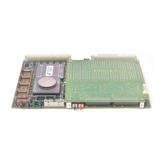
A detailed hardware functional description, including front panel switches and indicators Memory maps General Description The MVME167, based on the MC68040 microprocessor, is a high- functionality VMEbus-based solution for scientific and industrial embedded-controller applications. It features: Onboard memory expansion mezzanine module with... -
Page 24: Onboard Memory Mezzanine Module
Board Level Hardware Description Onboard Memory Mezzanine Module The MVME167 onboard DRAM mezzanine boards are available in different sizes and with programmable parity protection or Error Checking and Correction (ECC) protection. The main board and a single mezzanine board together take one slot. -
Page 25: Serial Ports
A functional description of the Printer Port interface starts on page 2-20. Ethernet Transceiver Interface The Ethernet transceiver interface is located on the MVME167, and the industry standard connector is located on the MVME712X transition module. A functional description of the Ethernet Interface starts on page... -
Page 26: 167Bug Firmware
Board Level Hardware Description 167Bug Firmware The MVME167Bug debug monitor firmware (167Bug) is provided in two of the four EPROM sockets on the MVME167. It provides: Over 50 debug commands Up/down load commands Disk bootstrap load commands A full set of onboard diagnostics... - Page 27 Features switches RESET ABORT Four 32-bit tick timers for periodic interrupts Watchdog timer Eight software interrupts Ð SCSI Bus interface with DMA Ð Four serial ports with EIA-232-D buffers with DMA Ð Centronics printer port Ð Ethernet transceiver interface with DMA VMEbus interface Ð...
-
Page 28: Speciþcations
Board Level Hardware Description Specifications Table 2-1. MVME167 General Specifications Characteristics SpeciÞcations Power requirements +5 Vdc (+/- 5%) 3.5 A (typical), 4.5 A (max.) (with all four EPROM sockets (at 25 MHz, with 32MB parity DRAM) populated and excluding 5.0 A (typical), 6.5 A (max.) -
Page 29: Board Level Overview
P2 rows A and C provide the connection to the SCSI bus, serial ports, Ethernet, and printer. Adapters I/O on the MVME167 is connected to the VMEbus P2 connector. The main board is connected to the transition modules through a P2 adapter board and cables. -
Page 30: Transition Modules
MVME712B Transition Modules and LCP2 Adapter Board User's Manual. ASICs The MVME167 board features several Application Specific Integrated Circuits (ASICs) including: VMEchip2 PCCchip2 MEMC040 MCECC All programmable registers in the MVME167 that reside in ASICs are covered in the Single Board Computers Programmer's Reference Guide. -
Page 31: Vmechip2 Asic
Board Level Overview VMEchip2 ASIC Provides the VMEbus interface. The VMEchip2 includes: Two tick timers A watchdog timer Programmable map decoders for the master and slave interfaces, and a VMEbus to/from local bus DMA controller A VMEbus to/from local bus non-DMA programmed access interface A VMEbus interrupter A VMEbus system controller... -
Page 32: Memc040 Memory Controller Asic
MCECC Memory Controller ASIC The MCECC memory controller ASIC provides the programmable interface for the ECC-protected DRAM mezzanine board. Functional Description The major functional blocks of the MVME167 covered in this section are: Front panel switches and LED indicators Data bus structure... -
Page 33: Front Panel Switches And Leds
STAT LED lights when the local bus TIP* signal line is low. This Green indicates one of the local bus masters is executing a local bus cycle. LED lights when the MVME167 is the VMEbus system SCON Green SCON controller. -
Page 34: Data Bus Structure
Board Level Hardware Description Data Bus Structure The local data bus on the MVME167 is a 32-bit synchronous bus that is based on the MC68040 bus, and supports burst transfers and snooping. Local Bus Arbitration The various local bus master and slave devices use the local bus to communicate. -
Page 35: Eprom
Map decoder Access time When accessible at address 0 Static RAM The MVME167 includes 128KB of 32-bit wide 100 ns static RAM (SRAM), which: Supports 8-, 16-, and 32-bit wide accesses Allows the debugger operation and execution of limited diagnostics without the DRAM mezzanine Is controlled by the VMEchip2;... -
Page 36: Optional Sram Battery Backup
Board Level Hardware Description Optional SRAM Battery Backup SRAM battery backup is optionally available on the MVME167, but only as a factory build and only by special request. (Contact your local Motorola sales office for details.) The battery backup function is provided by a Dallas DS1210S nonvolatile controller chip and a Sanyo CR2430 battery. -
Page 37: Onboard Dram
Note the battery polarity and press the battery into the socket. Onboard DRAM The MVME167 onboard DRAM is located on a mezzanine board. The mezzanine boards are available in different sizes and with parity protection or ECC protection. Parity mezzanines are only supported on 25MHz main Note boards. -
Page 38: Stacking Mezzanines
Board Level Hardware Description Motorola software does support mixed parity and ECC memory boards on the same main board. The DRAM is four-way interleaved to efficiently support cache burst cycles. Onboard DRAM mezzanines are available in these configurations: 4, 8, 16, or 32MB with parity protection... -
Page 39: Battery Backed Up Ram And Clock
Functional Description Battery Backed Up RAM and Clock The MK48T08 RAM and clock chip is a 28-pin package that provides: A time-of-day clock An oscillator A crystal Power fail detection Memory write protection 8KB of RAM A battery The clock provides Seconds, minutes, hours, day, date, month, and year in BCD 24-hour format Automatic corrections for 28-, 29- (leap year), and 30-day... -
Page 40: Vmebus Interface
The I/O interface configuration headers are located on the MVME167 and the MVME712X transition module. The I/O on the MVME167 is connected to the VMEbus P2 connector. The MVME712X transition module is connected to the MVME167 through cables and a P2 adapter board. - Page 41 Functional Description All four serial ports use EIA-232-D drivers and receivers located on the MVME167, and all the signal lines are routed to the I/O connector. Serial port 1 is a minimum function asynchronous port. It uses RXD, CTS, TXD, and RTS.
-
Page 42: Parallel Port Interface
Board Level Hardware Description Parallel Port Interface The PCCchip2 provides an 8-bit bidirectional parallel port. This port may be used as a Centronics-compatible parallel printer port or as a general parallel I/O port. All eight bits of the port must be either inputs or outputs (no individual bit selection). -
Page 43: Ethernet Interface
Every MVME167 is assigned an Ethernet Station Address. The address is $08003E2xxxxx where xxxxx is the unique 5-nibble number assigned to the board (i.e., every MVME167 has a different value for xxxxx). Each module has the Ethernet Station Address displayed on a label attached to the VMEbus P2 connector. -
Page 44: Scsi Interface
Refer to the 82596CA user's guide for detailed programming information. SCSI Interface The MVME167 provides for mass storage subsystems through the industry-standard SCSI bus. These subsystems may include hard and floppy disk drives, streaming tape drives, and other mass storage devices. -
Page 45: Local Resources
Local Bus Timeout The MVME167 provides a timeout function for the local bus. When the timer is enabled and a local bus access times out, a Transfer Error Acknowledge (TEA) signal is sent to the local bus master. The timeout value is selectable by software for 8 µsec, 64 µsec, 256 µsec,... -
Page 46: Memory Maps
The normal address range is defined by the Transfer Type (TT) signals on the local bus. On the MVME167, Transfer Types 0, 1, and 2 define the normal address range. Table 2-5 on page 2-25 is the entire map from $00000000 to $FFFFFFFF. -
Page 47: Local Bus Memory Map
Memory Maps Table 2-5. Local Bus Memory Map Software Address Port Devices Accessed Size Cache Notes Range Size Inhibit $00000000 - User Programmable DRAMSIZE 1, 2 DRAMSIZE (Onboard DRAM) DRAMSIZE - User Programmable 3, 4 D32/D16 $FF7FFFFF (VMEbus) $FF800000 - $FFBFFFFF $FFC00000 - reserved... -
Page 48: Local I/O Devices Memory Map
Board Level Hardware Description The following table focuses on the Local I/O Devices portion of the local bus Main Memory Map. Table 2-6. Local I/O Devices Memory Map Address Range Devices Accessed Port Size Size Notes $FFF00000 - $FFF3FFFF reserved 256KB $FFF40000 - $FFF400FF VMEchip2 (LCSR) - Page 49 Computers Programmer's Reference Guide or to the data sheet for the specific chip. 2. On the MVME167 this area does not return an acknowledge signal. If the local bus timer on the MVME167 is enabled, the access times out and is terminated by a TEA signal.
-
Page 50: Vmebus Memory Map
The VMEchip2 includes a user-p87grammable map decoder for the VMEbus to local bus interface. The map decoder allows you to program the starting and ending address and the modifiers the MVME167 responds to. VMEbus Short I/O Memory Map The VMEchip2 includes a user-programmable map decoder for the GCSR. -
Page 51: This Chapter Covers
This chapter provides instructions on: Unpacking the equipment Preparing the hardware Installing the MVME167 CISC Single Board Computer Note that hardware preparation instructions for the MVME712X transition module are provided in separate userÕs manuals for each model. Refer to the userÕs manual you received with your MVME712X. -
Page 52: Overview Of Startup Procedure
Disconnect AC power cable. manual you 3-13 received with Remove chassis cover. your chassis Remove Þller panels from card slots. Install your MVME167 in the chassis. Installing Transition Remove IACK and BG jumpers from Modules and backplane. 3-15 Adapter Boards Slide the module into the chassis and fasten it securely. - Page 53 Overview of Startup Procedure Table 3-1. Startup Overview (Continued) Stage What you will need to do... Refer to... page... Install adapter boards and transition modules. Transition Modules and 3-16 Adapter Boards Overview Installing Transition 3-19 Modules and Adapter Boards Set jumpers on the transition module(s). The userÕs manual you Connect and install the MVME712X received with your...
- Page 54 Note that the debugger prompt appears. Powering Up the 3-24 System Starting Up 167Bug You may also wish to obtain the Debugging Package for Motorola 68k CISC CPUs UserÕs Manual and the 167Bug Diagnostics UserÕs Manual Examine and/or change environmental Examining parameters. and/or Changing...
-
Page 55: Preparing The Hardware
Preparing the system chassis Modifying Configuration before Installation To select the desired configuration and ensure proper operation of the MVME167, certain option modifications may be necessary before installation. The location of the switches, jumper headers, connectors, and LED indicators on the MVME167 is illustrated in Figure 3-1. -
Page 56: Hardware Preparation And Installation
Hardware Preparation and Installation MVME FAIL STAT RUN SCON +12V SCSI VME ABORT RESET Figure 3-1. MVME167 Switches, Headers, Connectors, Fuses, and LEDs... -
Page 57: Checking The 167Bug Eproms
There are two spare EPROM sockets, XU3 and XU4, available to carry user-programmed EPROMs. Jumper Settings The MVME167 has been factory tested and is shipped with the factory jumper settings described in the following sections. The MVME167 operates with its required and factory-installed Debug... -
Page 58: Optional Jumper Settings
General Purpose Software Readable Header J1 Each MVME167 may be configured with readable jumpers. They can be read as a register (at $FFF40088) in the VMEchip2 LCSR. The bit values are read as a one when the jumper is off, and as a zero when the jumper is on. - Page 59 Preparing the Hardware Table 3-2. J1 Bit Descriptions J1 Pins Description Bit #0 (GPI0) When this bit is a one (high), it instructs the debugger to use local Static RAM for its work page (i.e., variables, stack, vector tables, etc.). This bit will be high when jumper is removed. Bit #1 (GPI1) When this bit is a one (high), it instructs the debugger to use the default setup/operation parameters in ROM versus the...
-
Page 60: System Controller Header J2
Serial Port 4 Clock Configuration Select Headers J6 and J7 Serial port 4 can be configured to use clock signals provided by the RTXC4 and TRXC4 signal lines. Headers J6 and J7 on the MVME167 configure serial port 4 to drive or receive RTXC4 and TRXC4, respectively (see Table 3-5). - Page 61 Preparing the Hardware The remaining configuration of the clock lines is accomplished using the Serial Port 4 Clock Configuration Select header on the MVME712M transition module. Refer to the MVME712M Transition Module and P2 Adapter Board User's Manual for configuration of that header. Table 3-5.
-
Page 62: Optional Sram Backup Power Source Select Header J8
Optional SRAM Backup Power Source Select Header J8 Header J8 is an optional header used to select the SRAM backup power source on the MVME167, if the optional battery is present. (The battery backup for SRAM is optionally available, but only as a factory build and only by special request.) -
Page 63: Preparing The Mvme167 For Installation
Preparing the Hardware Preparing the MVME167 for Installation Refer to the setup procedures in the manuals for your particular chassis or system for additional details concerning the installation of the MVME167 into a VME chassis. Table 3-7. MVME167 Preparation Procedure Step Action... -
Page 64: Preparing The System Chassis
Hardware Preparation and Installation Preparing the System Chassis Now that the MVME167 is ready for installation, prepare the system chassis and determine slot assignments (for peripherals, transition modules, etc.) as follows: Inserting or removing modules while power is applied could result in damage to module components. -
Page 65: Installing The Hardware
SCSI drives, and serial or parallel printers Installing the MVME167 in the Chassis Note that if the MVME167 is to be used as system controller, it must installed in the left-most card slot (slot 1), otherwise it may be installed in any unused double-height card slot. -
Page 66: Transition Modules And Adapter Boards Overview
MVME712X transition modules provide configuration headers and industry-standard connectors for internal and external I/O devices. The I/O on the MVME167 is connected to the VMEbus P2 connector. The MVME712X transition module is connected to the MVME167 through cables and a P2 adapter board as shown Figure 3-2 on page 3-17. - Page 67 Installing the Hardware MVME712X TERMINATOR MVME167 LC P2 ADAPTER J2, P2, OR J11 ENCLOSURE BOUNDARY Figure 3-2. Typical Internal SCSI and Serial Port Connections 3-17...
-
Page 68: Equipment Connections
Hardware Preparation and Installation Equipment Connections Some connection diagrams are in the Single Board Computer Programmer's Reference Guide. The MVME712X transition modules and P2 adapter boards connect peripheral equipment to the MVME167 as shown in Table 3-10: Table 3-10. Peripheral Connections Equipment Type Connect Through... -
Page 69: Installing Transition Modules And Adapter Boards
SCSI devices. Connecting Peripherals The MVME167 mates with (optional) terminals or other peripherals at the EIA-232-D serial ports (marked SERIAL PORTS 1, 2, 3, and 4 on the MVME712X transition module), parallel port, SCSI ports, and LAN Ethernet port, as shown in Figure 3-4 on page 3-22. -
Page 70: Peripheral Connection Procedures
EIA-232-D port connectors with the appropriate cables and conÞguration After powerup, these ports can be reconÞgured by programming the MVME167 CD2401 Serial Controller Chip (SCC), or by using the 167Bug PF command. Set up the device serial ports as described in Step ConÞguring a Port under... - Page 71 XON/XOFF handshaking is enabled. Refer to Configuring a Port under the PF (Port Format) command in the Debugging Package for 68K CISC CPUs UserÕs Manual. MVME712B MVME712X MVME167 P2 ADAPTER ENCLOSURE BOUNDARY Figure 3-3. Using MVME712A/AM and MVME712B 3-21...
- Page 72 Hardware Preparation and Installation MVME 712A/12/13 MVME 712B To J10 on Transition Module MVME 712A MVME (MVME712M 712B similar) (if used) Optional Modem Port To J2 on Adapter Board Figure 3-4. Typical Transition Module Peripheral Port Connectors 3-22...
-
Page 73: Completing The Installation
Installing the Hardware Completing the Installation Table 3-13. Installation Completion Procedure Step Action... Reassemble the chassis. Reconnect the AC power. Starting the System After completing the preparation and installation procedures, you are ready to start up your system. Table 3-14. System Startup Overview Stage What you will need to do... -
Page 74: Powering Up The System
Hardware Preparation and Installation Powering Up the System The following table shows what takes place when you turn equipment power ON (depending on whether 167Bug is in Board Mode or System Mode): If 167Bug is in... Board Mode 167Bug executes some self-checks and displays the debugger prompt 167-Bug>... -
Page 75: Programming The Pccchip2 And Vmechip2
Installing the Hardware Table 3-15. RTC Initialization Procedure Step Action Board Mode System Mode Allow 167Bug to boot up normally. Stop the auto-boot sequence by pressing the <BREAK> key. (If the system has already started and failed a conÞdence test in system mode, you should be in the debugger menu). -
Page 76: System Considerations
System Considerations Backplane Power Connections The MVME167 needs to draw power from both P1 and P2 of the VMEbus backplane. P2 is also used for the upper 16 bits of data for 32-bit transfers, and for the upper 8 address lines for extended addressing mode. -
Page 77: Multiple Module Cage Configuration
One register of the GCSR set includes four bits which function as location monitors to allow one MVME167 processor to broadcast a signal to other MVME167 processors, if any. All eight of the GSCR registers are accessible from any local processor as well as from the VMEbus. -
Page 78: Scsi Bus Termination
Hardware Preparation and Installation SCSI Bus Termination The MVME167 provides SCSI terminator power through a 1- amp fuse (F1) located on the P2 adapter board. The fuse is socketed. If the fuse is blown, the SCSI devices may not operate or may function erratically. -
Page 79: This Chapter Covers
The M68000 firmware family provides a high degree of functionality and user friendliness, and yet stresses portability and ease of maintenance. This member of the M68000 firmware family is implemented on the MVME167 CISC Single Board Computer, and is known as the MVME167Bug, or just 167Bug. -
Page 80: Description Of 167Bug
Debugger General Information Description of 167Bug The 167Bug package, MVME167Bug, is a powerful evaluation and debugging tool for systems built around the MVME167 CISC-based microcomputers. 167Bug consists of three parts: The ÒdebuggerÓ or Ò167BugÒ; a command-driven user- interactive software debugger, described in Chapter 5... -
Page 81: Debugger Or Diagnostic Directories
Introduction to MVME167Bug Debugger or Diagnostic Directories When using 167Bug, you operate out of either the debugger directory or the diagnostic directory. With the If you are in ... You have available ... prompt ... All of the debugger The debugger directory 167-Bug>... -
Page 82: Similarity To Other Motorola Debugging Firmware
Debugger General Information Similarity to other Motorola Debugging Firmware If you have used one or more of Motorola's other debugging packages, you will find the CISC 167Bug very similar. Some effort has also been made to make the interactive commands more consistent. -
Page 83: Memory Requirements
167Bug stack and static variable space and the rest is reserved as user space. Whenever the MVME167 is reset, the target PC is initialized to the address corresponding to the beginning of the user space, and the target stack pointers are initialized to addresses within the user space, with the target Interrupt Stack Pointer (ISP) set to the top of the user space. -
Page 84: Starting Up 167Bug
Debugger General Information Starting Up 167Bug 1. Verify that the MVME167 is properly installed and operating as described in Table 3-1 on page 3-2. 2. Power up the system. 167Bug executes some self-checks and displays the debugger prompt (if 167Bug is in 167-Bug>... -
Page 85: Romboot
Booting and Restarting 167Bug 4. Following this message there is a delay to allow you an opportunity to abort the Autoboot process if you wish. To gain control without Autoboot, you can press the BREAK or the software switches. ABORT RESET 5. -
Page 86: Network Boot
Your routine must pass a checksum test, which ensures that this routine was really intended to receive control at powerup. For complete details on how to use ROMboot, refer to the Debugging Package for Motorola 68K CISC CPUs User's Manual. Network Boot Network Auto Boot is a software routine contained in the 167Bug EPROMs that provides a mechanism for booting an operating system using a network (local Ethernet interface) as the boot device. -
Page 87: Restarting The System
Booting and Restarting 167Bug 3. At powerup, Network Boot is enabled, and providing the drive and controller numbers encountered are valid, the following message is displayed on the system console: "Network Boot in progress... To abort hit <BREAK>" Following this message there is a delay to allow you to abort the Network Boot process if you wish. -
Page 88: Reset
COLD and WARM reset modes are available. By default, 167Bug is in COLD mode. During COLD reset: 1. A total system initialization takes place, as if the MVME167 had just been powered up. 2. All static variables (including disk device and controller parameters) are restored to their default states. -
Page 89: Break
Booting and Restarting 167Bug Whenever abort is invoked when executing a user program (running target code), a "snapshot" of the processor state is captured and stored in the target registers. For this reason, abort is most appropriate when terminating a user program that is being debugged. -
Page 90: Sysfail* Assertion/Negation
Debugger General Information Break Sequence 1. Removes any breakpoints in your code and keeps the breakpoint table intact. 2. Takes a snapshot of the machine state if the function was entered using SYSCALL. This machine state is then accessible to you for diagnostic purposes. SYSFAIL* Assertion/Negation Upon a reset/powerup condition the debugger asserts the VMEbus SYSFAIL* line (refer to the VMEbus specification). -
Page 91: Disk I/O Support
Disk I/O Support Disk I/O Support 167Bug can initiate disk input/output by communicating with intelligent disk controller modules over the VMEbus. This section covers: Blocks Versus Sectors Device Probe Function Disk I/O via 167Bug Commands Disk I/O via 167Bug System Calls Default 167Bug Controller and Device Parameters Disk I/O Error Codes Disk Support Facilities... -
Page 92: Blocks Versus Sectors
Debugger General Information Blocks Versus Sectors The logical block defines the unit of information for disk devices. A disk is viewed by 167Bug as a storage area divided into logical blocks. By default, the logical block size is set to 256 bytes for every block device in the system. -
Page 93: Disk I/O Via 167Bug Commands
These following 167Bug commands are provided for disk I/O. Detailed instructions for their use are found in the Debugging Package for Motorola 68K CISC CPUs User's Manual. When a command is issued to a particular controller LUN and device LUN, these LUNs are remembered by 167Bug so that the next disk command defaults to use the same controller and device. -
Page 94: Bh (Bootstrap And Halt)
Refer to the Debugging Package for Motorola 68K CISC CPUs User's Manual for information on using these and other system calls. Controller Command Packets... -
Page 95: Default 167Bug Controller And Device Parameters
Refer to the system call descriptions in the Debugging Package for Motorola 68K CISC CPUs User's Manual for details on the format and construction of these standardized "user" packets. The packets which a controller module expects to be given vary from controller to controller. -
Page 96: Disk I/O Error Codes
Debugger General Information There are three ways to change the parameter tables: When you invoke one of Change Using ... If a cold-start reset occurs ... these commands ... status is ... Command The conÞguration area of Temporary The default parameter BO or BH the disk is read and the information is written back... -
Page 97: Network I/O Support
Network I/O Support Network I/O Support The Network Boot Firmware provides the capability to boot the CPU through the ROM debugger using a network (local Ethernet interface) as the boot device. The booting process is executed in two distinct phases. The first phase allows the diskless remote node to discover its network identify and the name of the file to be booted. -
Page 98: Rarp/Arp Protocol Modules
Debugger General Information RARP/ARP Protocol Modules The Reverse Address Resolution Protocol (RARP) basically consists of an identity-less node broadcasting a "whoami" packet onto the Ethernet, and waiting for an answer. The RARP server fills an Ethernet reply packet up with the target's Internet Address and sends it. -
Page 99: Network I/O Error Codes
167Bug returns an error code if an attempted network operation is unsuccessful. Multiprocessor Support The MVME167 dual-port RAM feature makes the shared RAM available to remote processors as well as to the local processor. This can be done by either of the following two methods:... -
Page 100: Mpcr Status Codes
Debugger General Information MPCR Status Codes The status codes stored in the MPCR are of two types: Status returned (from the 167Bug) Command set by the bus master (job requested by some processor) The status codes that may be returned from 167Bug are: (HEX 00) Wait. - Page 101 Multiprocessor Support 3. As the initialization proceeds, the execution path comes to the "prompt" routine. Before sending the prompt, this routine places an R in the MPCR to indicate that initialization is complete. Then the prompt is sent. Ð If no terminal is connected to the port, the MPCR is still polled to see whether an external processor requires control to be passed to the dual-port RAM.
-
Page 102: Global Control And Status Register (Gcsr) Method
2. The remote processor then sets bit 8 (SIG0) of the VMEchip2 LM/SIG register. 3. This causes the MVME167 to install breakpoints and begin execution. The result is identical to the MPCR method (with status code B) described in the previous section. -
Page 103: Diagnostic Facilities
Included in the 167Bug package is a complete set of hardware diagnostics intended for testing and troubleshooting of the MVME167. These diagnostics are completely described in the MVME167Bug Debugging Package User's Manual. In order to use the diagnostics, you must switch directories to the diagnostic directory. - Page 104 Debugger General Information Table 4-1. Diagnostic Monitor Commands/Prefixes Command/ Description PreÞx Non-Verbose Mode Switch Directories Stop on Error Mode Selftest Clear (Zero) Error Counters Zero Pass Count Table 4-2. Diagnostic Utilities Command Description Write loop enable Read loop enable 4-26...
-
Page 105: 167Bug Diagnostic Test Groups
Diagnostic Facilities 167Bug Diagnostic Test Groups Refer to the MVME167Bug Debugging Package User's Manual for complete descriptions of the diagnostic routines available and instructions on how to invoke them. Note that some diagnostics depend on restart defaults that are set up only in a particular restart mode. - Page 106 Debugger General Information 4-28...
-
Page 107: This Chapter Covers
5Using the 167Bug Debugger This Chapter Covers Entering debugger command lines Entering and debugging programs Calling system utilities from user programs Preserving the debugger operating environment Floating point support The 167Bug debugger command set Entering Debugger Command Lines 167Bug is command-driven and performs its various operations in response to user commands entered at the keyboard. - Page 108 Using the 167Bug Debugger The presence of the upward caret ( ^ ) before a Note character indicates that the Control (CTRL) key must be held down while striking the character key. (cancel line) The cursor is backspaced to the beginning of the line. (backspace) The cursor is moved back one position.
-
Page 109: Debugger Command Syntax
Entering Debugger Command Lines For example, if a breakpoint has been specified, then control returns to the debugger when the breakpoint is encountered during execution of the user program. Alternately, the user program could return to the debugger by means of the TRAP #15 function ".RETURN". -
Page 110: Syntactic Variables
Using the 167Bug Debugger Syntactic Variables The following syntactic variables are encountered in the command descriptions which follow. In addition, other syntactic variables may be used and are defined in the particular command description in which they occur. Delimiter; either a comma or a space. Expression (described in detail in a following section). -
Page 111: Address As A Parameter
Entering Debugger Command Lines A numeric value may also be expressed as a string literal of up to four characters. The string literal must begin and end with the single quote mark ('). The numeric value is interpreted as the concatenation of the ASCII values of the characters. -
Page 112: Address Formats
Using the 167Bug Debugger Address Formats Table 5-1 summarizes the address formats that are acceptable for address parameters in debugger command lines. Table 5-1. Debugger Address Parameter Formats Format Example Description Absolute address+contents of automatic offset register. N+Rn 130+R5 Absolute address+contents of the speciÞed offset register (not an assembler-accepted syntax). -
Page 113: Offset Registers
Entering Debugger Command Lines In commands with range specified as addr del addr, and Note with size option W or L chosen, data at the second (ending) address is acted on only if the second address is a proper boundary for a word or longword, respectively. - Page 114 Using the 167Bug Debugger Example: A portion of the listing file of an assembled, relocatable module is shown below: MOVE STRING SUBROUTINE 0 00000000 48E78080 MOVESTR MOVEM.L D0/A0,—(A7) 0 00000004 4280 CLR.L 0 00000006 1018 MOVE.B (A0)+,D0 0 00000008 5340 SUBQ.W #1,D0 0 0000000A 12D8...
-
Page 115: Port Numbers
MVME167 P2 connector). Sometimes known as the "console port", it is used for interactive user input/output by default. 2. MVME167 EIA-232-D (Terminal Port 1 or 01) (PORT 2 on the MVME167 P2 connector). Sometimes known as the "host port", this is the default for downloading, uploading, concurrent mode, and transparent modes. -
Page 116: Entering And Debugging Programs
1. Enter the program one source line at a time. 2. After each source line is entered, it is assembled and the object code is loaded to memory. Refer to the Debugging Package for Motorola 68K CISC CPUs User's Manual for complete details of the 167Bug Assembler/Disassembler. -
Page 117: Read The Program From Disk
MVME167 port 1. (Hardware configuration details are provided in Connecting Peripherals on page 3-19.) The file is downloaded from the host to MVME167 memory by the Load (LO) command. Read the Program from Disk Another way to enter a program is by reading the program from disk, using one of the disk commands (BO, BH, IOP). -
Page 118: 167Bug Vector Table And Workspace
Using the 167Bug Debugger 167Bug uses certain of the MVME167 onboard resources and may also use offboard system memory to contain temporary variables, exception vectors, etc. If you disturb resources upon which 167Bug depends, then the debugger may function unreliably or not at all. -
Page 119: Examples
Preserving the Debugger Operating Environment Examples If, for example, your program inadvertently wrote over the static variable area containing the serial communication parameters, these parameters would be lost, resulting in a loss of communication with the system console terminal. If your program corrupts the system stack, then an incorrect value may be loaded into the processor Program Counter (PC), causing a system crash. - Page 120 Using the 167Bug Debugger Table 5-2. Exception Vectors Used by 167Bug (Continued) Vector Exception 167Bug Facility Offset TRAP #15 System calls NOTE Level 7 interrupt ABORT pushbutton NOTE Level 7 interrupt AC Fail FP Unimplemented Data Software emulation and data Type type conversion of ßoating point data.
-
Page 121: Example: Trace One Instruction Using Debugger
Preserving the Debugger Operating Environment Example: Trace one instruction using debugger. 167Bug> =00010000 SR =2700=TR:OFF_S._7_..VBR =00000000 USP =0000DFFC MSP =0000EFFC ISP* =0000FFFC SFC =0=F0 DFC =0=F0 CACR =0=..=00000000 D1 =00000000 D2 =00000000 D3 =00000000 =00000000 D5 =00000000 D6 =00000000 D7 =00000000 =00000000 A1... -
Page 122: Creating A New Vector Table
Using the 167Bug Debugger The start address of this target vector table area is the base address ($00) of the debugger memory. This address is loaded into the target-state VBR at powerup and cold-start reset and can be observed by using the RD command to display the target-state registers immediately after powerup. -
Page 123: 167Bug Generalized Exception Handler
Preserving the Debugger Operating Environment EXCEPT - Exception handler **** EXCEPT SUBQ.L #4,A7 Save space in stack for a PC value. LINK A6,#0 Frame pointer for accessing PC space. MOVEM.L A0-A5/D0-D7,-(SP) Save registers. : decide here if your code handles exception, if so, branch... MOVE.L BUFVBR,A0 Pass exception to debugger;... -
Page 124: Floating Point Support
Using the 167Bug Debugger It may turn out that your program uses one or more of the exception vectors that are required for debugger operation. Debugger facilities may still be used, however, if your exception handler can determine when to handle the exception itself and when to pass the exception to the debugger. - Page 125 Floating Point Support Valid data types that can be used when modifying a floating point data register or a floating point memory location: Integer Data Types Byte 1234 Word 12345678 Longword Floating Point Data Types 1_FF_7FFFFF Single Precision Real Format 1_7FF_FFFFFFFFFFFFF Double Precision Real Format 1_7FFF_FFFFFFFFFFFFFFFF...
-
Page 126: Single Precision Real
Using the 167Bug Debugger Single Precision Real This format would appear in memory as: 1-bit sign Þeld (1 binary digit) 8-bit biased exponent Þeld (2 hex digits. Bias = $7F) 23-bit fraction Þeld (6 hex digits) A single precision number takes 4 bytes in memory. Double Precision Real This format would appear in memory as: 1-bit sign Þeld... -
Page 127: Packed Decimal Real
Floating Point Support Packed Decimal Real This format would appear in memory as: 4-bit sign Þeld (4 binary digits) 16-bit exponent Þeld (4 hex digits) 68-bit mantissa Þeld (17 hex digits) A packed decimal number takes 12 bytes in memory. Scientific Notation This format provides a convenient way to enter and display a floating point decimal number. -
Page 128: The 167Bug Debugger Command Set
Using the 167Bug Debugger The 167Bug Debugger Command Set The 167Bug debugger commands are summarized in Table 5-3. The command syntax is shown using the symbols explained earlier in this chapter. The CNFG and ENV commands are explained in Appendix A. Controllers, devices, and their LUNs are listed in Appendix B or Appendix C. - Page 129 The 167Bug Debugger Command Set Table 5-3. Debugger Commands (Continued) Command Title Command Line Syntax Mnemonic Data Conversion DC exp | addr [; [B][O][A]] DMA Block of Memory DMA range del addr del vdir del am del blk Move [; B|W|L] One Line Disassembler DS addr [:count | del addr] Dump S-records...
- Page 130 Using the 167Bug Debugger Table 5-3. Debugger Commands (Continued) Command Title Command Line Syntax Mnemonic Load Macros MAR [controller LUN] [del [device LUN] [del block #]] Memory Display MD [S] addr [:count | del addr] [; [B|W|L|S|D|X|P|DI]] MENU Menu MENU Memory Modify MM addr [;...
- Page 131 The 167Bug Debugger Command Set Table 5-3. Debugger Commands (Continued) Command Title Command Line Syntax Mnemonic RESET Cold/Warm Reset RESET Read Loop RL addr; [B|W|L] Register Modify RM [reg] [; [S|D]] Register Set RS reg [del exp|del addr] [; [S|D]] Switch Directories Set Time and Date SET mmddyyhhmm | n;...
- Page 132 Using the 167Bug Debugger 5-26...
-
Page 133: This Appendix Covers
This command is used to display and configure the board information block. This block is resident within the Non-Volatile RAM (NVRAM). Refer to the MVME167 Single Board Computer User's Manual for the actual location. The information block contains various elements detailing specific operation parameters of the hardware. - Page 134 Configure and Environment Commands Example: to display the current contents of the board information block. cnfg 167-Bug> Board (PWA) Serial Number = "000000061050" Board Identifier = "MVME167-03 " Artwork (PWA) Identifier = "01-W3826B03A " MPU Clock Speed = "2500" Ethernet Address...
-
Page 135: Setting Environment To Bug/Operating System
Setting Environment to Bug/Operating System Once modification and update is complete, you can now display the current contents as described earlier. Setting Environment to Bug/Operating System ENV [;[D]] The Environment (ENV) command allows you to interactively view and configure all Bug operational parameters that are kept in Battery Backed Up RAM (BBRAM), also known as Non-Volatile RAM (NVRAM). - Page 136 Configure and Environment Commands The parameters to be configured are listed in the following table: Table A-1. ENV Command Parameters ENV Parameter and Options Default Meaning of Default Bug or System environment [B/S] System mode Field Service Menu Enable [Y/N] Display Þeld service menu.
- Page 137 Setting Environment to Bug/Operating System Table A-1. ENV Command Parameters (Continued) ENV Parameter and Options Default Meaning of Default Auto Boot Abort Delay This is the time in seconds that the Auto Boot sequence will delay before starting the boot. The purpose for the delay is to allow you the option of stopping the boot by use of the Break key.
- Page 138 Configure and Environment Commands Table A-1. ENV Command Parameters (Continued) ENV Parameter and Options Default Meaning of Default Network Auto Boot Controller LUN of a network controller module currently supported by the Bug. Default is 00. Network Auto Boot Device LUN LUN of a network device currently supported by the Bug.
- Page 139 This must be a multiple of the debugger work page, modulo $10000 (64KB). In a multi-167 environment, each MVME167 could be set to start its work page at a unique address to allow multiple debaters to operate simultaneously...
- Page 140 Memory Search Delay Address FFFFCE0F The process of using the Memory Search Delay Address was implemented on the MVME188. It has not been used on the MVME167. Memory Size Enable [Y/N] Memory will be sized for Self Test diagnostics. Memory Size Starting Address 00000000 Default Starting Address is $0.
- Page 141 Slave address decoders setup. The slave address decoders are used to allow another VMEbus master to access a local resource of the MVME167. There are two slave address decoders. They are set up as follows. Slave Enable #1 [Y/N] Yes, Setup and enable the Slave Address Decoder #1.
- Page 142 Configure and Environment Commands Table A-1. ENV Command Parameters (Continued) ENV Parameter and Options Default Meaning of Default Slave Address Translation 00000000 This register deÞnes which bits of the Select #1 Translation Address are signiÞcant. A logical one "1" indicates signiÞcant address bits, logical zero "0"...
- Page 143 Setting Environment to Bug/Operating System Table A-1. ENV Command Parameters (Continued) ENV Parameter and Options Default Meaning of Default Master Enable #1 [Y/N] Yes, Setup and enable the Master Address Decoder #1. Master Starting Address #1 02000000 Base address of the VMEbus resource that is accessible from the local bus.
- Page 144 Configure and Environment Commands Table A-1. ENV Command Parameters (Continued) ENV Parameter and Options Default Meaning of Default Master Enable #4 [Y/N] Do not set up and enable the Master Address Decoder #4. Master Starting Address #4 00000000 Base address of the VMEbus resource that is accessible from the local bus.
- Page 145 MVME187) or $04=145 ns (33 MHz MVME187). Static RAM Speed Code Used to set up the SRAM speed. Default is $01 = 125 ns (25 MHz MVME167) or $00=115 ns (33 MHz MVME187) PCC2 Vector Base Base interrupt vector for the VMEC2 Vector Base #1 component speciÞed.
- Page 146 Configure and Environment Commands A-14...
-
Page 147: Disk/Tape Controller Modules Supported
Second Address and can be called up by Second CLUN. First First Second Second Controller Type CLUN Address CLUN Address CISC Single Board Computer (MVME167) MVME320 - Winchester/Floppy $FFFFB000 $FFFFAC00 Controller MVME323 - ESDI Winchester $FFFFA000 $FFFFA200 Controller MVME327A - SCSI Controller $FFFFA600 $FFFFA700... -
Page 148: Disk/Tape Controller Default Conþgurations
Disk/Tape Controller Data Disk/Tape Controller Default Configurations Note SCSI Common Command Set (CCS) devices are only the ones tested by Motorola Computer Group. CISC Single Board Computers -- 7 Devices Controller LUN Address Device LUN Device Type $XXXXXXXX SCSI Common Command Set... - Page 149 Disk/Tape Controller Default Configurations MVME327A -- 9 Devices Controller LUN Address Device LUN Device Type $FFFFA600 SCSI Common Command Set (CCS), which may be any of these: - Fixed direct access $FFFFA700 - Removable ßexible direct access (TEAC style) - CD-ROM - Sequential access Local ßoppy drive Local ßoppy drive...
-
Page 150: Iot Command Parameters For Supported Floppy Types
QIC-02 streaming tape drive $FFFF5100 IOT Command Parameters for Supported Floppy Types The following table lists the proper command parameters for floppies used with boards such as the MVME328, MVME167, and MVME187. Floppy Types and Formats IOT Parameter DSDD5 PCXT8... - Page 151 IOT Command Parameters for Supported Floppy Types Floppy Types and Formats IOT Parameter DSDD5 PCXT8 PCXT9 PCXT9_3 PCAT Single/Double TRACK Density Single/Equal_in_all Track Zero Density Slow/Fast Data Rate Other Characteristics Number of Physical 0A00 0280 02D0 05A0 0960 0B40 1680 Sectors Number of Logical 09F8...
- Page 152 Disk/Tape Controller Data...
-
Page 153: Network Controller Modules Supported
The controllers are accessed via the CLUNs and DLUNs specified in the following table: Table C-1. Network Controller Access Data Controller Interface CLUN DLUN Address Type Type MVME167 $FFF46000 Ethernet MVME376 $FFFF1200 Ethernet MVME376 $FFFF1400 Ethernet MVME376 $FFFF1600 Ethernet MVME376... - Page 154 Network Controller Data Table C-1. Network Controller Access Data (Continued) Controller Interface CLUN DLUN Address Type Type MVME376 $FFFFA400 Ethernet MVME374 $FF000000 Ethernet MVME374 $FF100000 Ethernet MVME374 $FF200000 Ethernet MVME374 $FF300000 Ethernet MVME374 $FF400000 Ethernet MVME374 $FF500000 Ethernet...
- Page 155 DTroubleshooting the MVME167: Solving Startup Problems Try these simple troubleshooting steps before calling for help or sending your CPU board back for repair. Some of the procedures will return the board to the factory debugger environment. (The board was tested under these conditions before it left the factory.)
- Page 156 Troubleshooting the MVME167: Solving Startup Problems Table D-1. Troubleshooting Steps (Continued) Possible Condition Try This: Problem II. There is a A. The Recheck the keyboard connections and power. display on the keyboard may terminal, but be connected input from the incorrectly.
- Page 157 Table D-1. Troubleshooting Steps (Continued) Possible Condition Try This: Problem III. Debug A. Debugger 1. Disconnect all power from your system. prompt EPROM may be 2. Check that the proper debugger EPROM is missing. 167-Bug> installed per this manual. B. The board does not appear 3.
- Page 158 Troubleshooting the MVME167: Solving Startup Problems Table D-1. Troubleshooting Steps (Continued) Possible Condition Try This: Problem IV. Debug A. The initial 1. Start the onboard calendar clock and timer. Type prompt debugger environment set mmddyyhhmm <Return> 167-Bug> parameters may where the characters indicate the month, day, appears at be set wrong.
- Page 159 Table D-1. Troubleshooting Steps (Continued) Possible Condition Try This: Problem 6. You may need to use the cnfg command (see Appendix A) to change clock speed and/or Ethernet Address, and then later return to env <Return> and step 3. 7. Run selftest by typing in st <Return>...
- Page 160 Troubleshooting the MVME167: Solving Startup Problems...
-
Page 161: Introduction
EEIA-232-D Interconnections Introduction The EIA-232-D standard is the most common terminal/computer and terminal/modem interface, and yet it is not fully understood This may be because not all the lines are clearly defined, and many users do not see the need to follow the standard in their applications. - Page 162 EIA-232-D Interconnections Table E-1. EIA-232-D Interconnections Signal Signal Name and Description Number Mnemonic CHASSIS GROUND. Not always used. See section Proper Grounding. TRANSMIT DATA. Data to be transmitted; input to the modem from the terminal. RECEIVE DATA. Data which is demodulated from the receive line;...
-
Page 163: Levels Of Implementation
Levels of Implementation Table E-1. EIA-232-D Interconnections (Continued) Signal Signal Name and Description Number Mnemonic RING INDICATOR. Output from the modem to the terminal; indicates to the terminal that an incoming call is present. The terminal causes the modem to answer the phone by carrying DTR true while RI is active. -
Page 164: Signal Adaptations
EIA-232-D Interconnections Signal Adaptations One set of handshaking signals frequently implemented are RTS and CTS. CTS is used in many systems to inhibit transmission until the signal is high. In the modem application, RTS is turned around and returned as CTS after 150 microseconds. RTS is programmable in some systems to work with the older type 202 modem (half duplex). - Page 165 Levels of Implementation SERIAL PORT 1488 1489A 39kΩ -12V CONNECTOR +12V LS08 TERMINAL 470Ω 470Ω 470Ω OPTIONAL HARDWARE TRANSPARENT MODE SIG GND CHASSIS GND LOGIC LS08 +12V SIG GND 470Ω 1488 SERIAL PORT 1489A CONNECTOR 39kΩ -12V MODEM 1488 HOST SYSTEM 470Ω...
- Page 166 EIA-232-D Interconnections Figure E-2 shows a way of wiring an EIA-232-D connector to enable a computer to connect to a basic terminal with only three lines. This is feasible because most terminals have DTR and RTS signals that are ON, and which can be used to pull up the CTS, DCD, and DSR signals.
-
Page 167: Proper Grounding
Levels of Implementation Proper Grounding Another subject to consider is the use of ground pins. There are two pins labeled GND. Pin 7 is the SIGNAL GROUND and must be connected to the distant device to complete the circuit. Pin 1 is the CHASSIS GROUND, but it must be used with care. - Page 168 EIA-232-D Interconnections...
- Page 169 Index Symbols application specific integrated circuits (ASICs) 2-8 +12V LED 2-11 arguments 5-3 Numerics arithmetic operators 5-4 167Bug (see debug monitor ASCII string 5-4 MVME167Bug) ASICs 2-8 command line 5-1 MCECC 2-10 command-line interface 2-4 MEMC040 2-10 debugger command set 5-22 PCCchip2 2-9 firmware 2-4 VMEchip2 2-9...
- Page 170 Index boldface strings 5-3 configuration, default disk/tape control- booting 167Bug 4-5 ler B-2 BOOTP protocol module 4-20 configuration, hardware 3-8 Bootstrap and Halt (BH) 4-16 Configure (CNFG) and Environment Bootstrap Operating System (BO) 4-15 (ENV) commands A-1 braces 5-3 Configure Board Information Block (CN- break 4-11 FG) A-1 BREAK key 4-11...
- Page 171 B-2 Ethernet modules supported B-1 interface 2-21 DLUN (device LUN) B-2, C-1 LAN (+12vdc) fuse 3-27 document set for MVME167-0xx 1-5 station address 2-21 documentation transceiver interface 2-3 additional manuals for this board 1-6 Ethernet (see 82596CA and LAN) 3-27,...
- Page 172 Index functions 5-13 interrupts 2-23 factory debugger environment D-1 preparation and installation 3-1 FAIL LED 2-11 headers 3-8 false 1-3 hexadecimal character 1-2 features 2-4 host port 5-9 general description 2-1 host system 5-10 flexible diskette B-2 floating point instructions 5-18 I/O interfaces 2-18 support 5-18 initialize the real time clock 3-24...
- Page 173 Multiprocessor Control Register (MPCR) local bus memory map 2-24, 2-25 Method 4-21 local bus timeout 2-23 multiprocessor support 4-21 local floppy drive B-3 MVME167 1-1, C-1 local I/O devices memory map 2-26 module installation 3-15 local resources 2-23 specifications 2-6 location monitors 3-27...
- Page 174 Real-Time Clock (RTC) 3-24 optional battery backup 2-14 related documentation 1-5 overview of M68000 firmware 4-1 relative address+offset 5-7 overview of MVME167 single board Remote Start Switch Method 4-21 computer 2-1 reset 4-10 overview of start-up procedure 3-2 RESET switch 2-11...
- Page 175 RTXC4 (Receive Transmit Clock 4) 3-10, for J6 and J7 serial port 4 clock con- 3-13 figuration select headers RUN LED 2-11 3-11 for J6 SRAM Optional Backup Power Select Header 3-12 Sanyo CR2430 battery 2-14 settings for SBC (see CISC Single Board Comput- J1 general purpose readable jumpers er(s)) B-1 (Serial...
- Page 176 3-9 timeout 2-23 transfer type (TT) 2-24 transition module installation 3-19 XON/XOFF 3-21 transition modules 2-8 supported by MVME167 board 2-8 TRAP #15 5-11 troubleshooting steps D-1 true 1-3 True/false bit state definitions 1-4 TRXC4 (Transmit Receive Clock 4) 3-10,...