
Related Manuals for Motorola MVME6100-0161


Summary of Contents for Motorola MVME6100-0161
- Page 1 MVME6100 Single-Board Computer Programmer’s Reference Guide V6100A/PG1 July 2004 Edition...
- Page 2 All rights reserved. Printed in the United States of America. Motorola and the stylized M logo are trademarks of Motorola, Inc., registered in the U.S. Patent and Trademark Office. All other product or service names mentioned in this document are the property of their...
- Page 3 The safety precautions listed below represent warnings of certain dangers of which Motorola is aware. You, as the user of the product, should follow these warnings and all other safety precautions necessary for the safe operation of the equipment in your operating environment.
- Page 4 Flammability All Motorola PWBs (printed wiring boards) are manufactured with a flammability rating of 94V-0 by UL-recognized manufacturers. EMI Caution This equipment generates, uses and can radiate electromagnetic energy. It Caution may cause or be susceptible to electromagnetic interference (EMI) if not installed and used with adequate EMI protection.
- Page 5 Warning Motorola Computer Group products with the CE marking comply with the EMC Directive (89/336/EEC). Compliance with this directive implies conformity to the following European Norms: EN55022 “Limits and Methods of Measurement of Radio Interference Characteristics...
- Page 6 Electronic versions of this material may be read online, downloaded for personal use, or referenced in another document as a URL to the Motorola Computer Group Web site. The text itself may not be published commercially in print or electronic form, edited, translated, or otherwise altered without the permission of Motorola, Inc.
-
Page 7: Table Of Contents
Contents About This Guide Overview of Contents ....................xiv Comments and Suggestions ..................xiv Conventions Used in This Manual ................xv CHAPTER 1 Board Description and Memory Maps Introduction ......................1-1 Overview ........................1-1 Memory Maps ......................1-5 Default Processor Memory Map ............... 1-5 MOTLoad’s Processor Memory Map ............... - Page 8 PCI Bus 0 Local Bus Devices ................. 2-15 Tsi148 ASIC ..................... 2-15 PCI6520 PMCSpan Bridge ..............2-15 MV64360 Interrupt Controller ................2-16 MV64360 Endian Issues ..................2-18 APPENDIX A Related Documentation Motorola Computer Group Documents ..............A-1 Manufacturers’ Documents ..................A-2 Related Specifications ..................... A-5 viii...
- Page 9 List of Figures Figure 1-1. MVME6100 Board Layout Diagram ........... 1-4 Figure 2-1. PCI Bus 1 Local Bus PMC Expansion Slots ........2-15...
- Page 10 Table 2-6. IDSEL Mapping for PCI Devices ............2-13 Table 2-7. PCI Arbitration Assignments for MV64360 ASIC ......2-14 Table 2-8. MV64360 Interrupt Assignments ............2-16 Table A-1. Motorola Computer Group Documents ..........A-1 Table A-2. Manufacturers’ Documents ..............A-2 Table A-3. Related Specifications ................A-5...
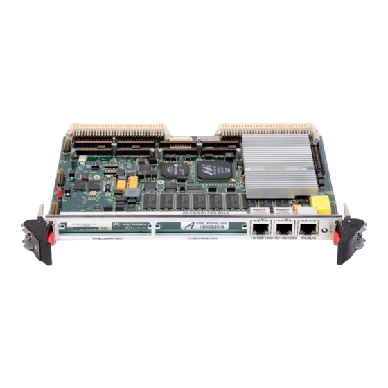
- Page 11 MVME6100 products. As of the printing date of this manual, the MVME6100 supports the models listed below. Model Number Description MVME6100-0161 1.267 GHz MPC7457 processor, 512MB DDR memory, 128MB Flash, Scanbe handles MVME6100-0163 1.267 GHz MPC7457 processor, 512MB DDR...
-
Page 12: Overview Of Contents
Documentation, provides a listing of related Motorola manuals, vendor documentation, and industry specifications. Comments and Suggestions Motorola welcomes and appreciates your comments on its documentation. We want to know what you think about our manuals and how we can make them better. Mail comments to:... -
Page 13: Conventions Used In This Manual
Conventions Used in This Manual The following typographical conventions are used in this document: bold is used for user input that you type just as it appears; it is also used for commands, options and arguments to commands, and names of programs, directories and files. -
Page 14: Introduction
PCI I/O memory map, and system I/O memory maps. Note Programmable registers in the MV64360 system controller are documented in a separate publication and obtainable from Motorola Computer Group by contacting your Field Area Engineer. Refer to Appendix A, Related Documentation, for more information on obtaining this documentation. -
Page 15: Table 1-1. Mvme6100 Features Summary
Board Description and Memory Maps The following table lists the features of the MVME6100. Table 1-1. MVME6100 Features Summary Feature Description Processor – Single 1.3 GHz MPC7457 processor – Bus clock frequency at 133 MHz – 36-bit address, 64-bit data buses –... - Page 16 – Supports 33/66 MHz, 32/64-bit PCI bus – Access through PCI6520 bridge to PMCspan Form Factor – Standard 6U VME Miscellaneous – Combined reset and abort switch – Status LEDs – 8-bit software-readable switch – VME geographical address switch http://www.motorola.com/computer/literature...
- Page 17 Board Description and Memory Maps IPMC ABT/RST 4248 0504 Figure 1-1. MVME6100 Board Layout Diagram Computer Group Literature Center Web Site...
-
Page 18: Memory Maps
Unassigned 2000 0000 21FF FFFF PCI Bus 1 I/O 2200 0000 23FF FFFF PCI Bus 1 Memory Space 0 2400 0000 25FF FFFF PCI Bus 1 Memory Space 1 2600 0000 27FF FFFF PCI Bus 1 Memory Space 2 http://www.motorola.com/computer/literature... - Page 19 Board Description and Memory Maps Table 1-2. Default Processor Address Map (continued) Processor Address Notes Start Size Definition 2800 0000 29FF FFFF PCI Bus 1 Memory Space 3 2A00 0000 41FF FFFF 384M Unassigned 4200 0000 4303 FFFF 256K MV64360 Integrated SRAM 4304 0000 F0FF FFFF 2783M...
-
Page 20: Motload's Processor Memory Map
Device CS1* I/O System Regs/NVRAM/RTC/UARTs F400 0000 F7FF FFFF Device CS0* Flash Bank A F800 0000 FBFF FFFF Device Boot Flash Bank B Note The internal registers only occupy the first 64KB, but minimum address decoding resolution is 1MB. http://www.motorola.com/computer/literature... -
Page 21: Default Pci Memory Map
Board Description and Memory Maps Default PCI Memory Map The MV64360 presents the following default PCI memory map after RESET negation. Note: it is the same as the GT-64260A with the addition of integrated SRAM. Table 1-4. Default PCI Address Map PCI Address Start Size... -
Page 22: Motload's Pci Memory Maps
The MVME6100 is fully capable of supporting both the PReP and the CHRP VME Memory Map examples with RAM size limited to 2 GB. System I/O Memory Map System resources including system control and status registers, NVRAM/RTC, and the 16550 UART are mapped into a 1 MB address http://www.motorola.com/computer/literature... -
Page 23: Table 1-6. Device Bank 1 I/O Memory Map
Board Description and Memory Maps range assigned to Device Bank 1. The memory map is defined in the following table: Table 1-6. Device Bank 1 I/O Memory Map Address Definition F110 0000 System Status Register 1 F110 0001 System Status Register 2 F110 0002 System Status Register 3 F110 0003... -
Page 24: System Status Register 1
ENV safe start. This bit reflects the current state of the ENV safe start select jumper. A set condition indicates that MOTLoad should provide the user the capability to select which Boot Image is used to boot the board, cleared MOTLoad should proceed with the first boot image found. http://www.motorola.com/computer/literature 1-11... - Page 25 Board Description and Memory Maps ABORT_L Abort. This bit reflects the current state of the onboard abort signal. This is a debounced version of the abort switch and may be used to determine the state of the abort switch. A set condition indicates that the abort switch is not depressed while a cleared condition would indicate that the abort switch is asserted.
-
Page 26: System Status Register 2
FLASH memory devices. Clearing this bit and disabling the HW write-protect will enable writes to the Bank A Flash devices. This bit is set during reset and must be reset by the system software to enable writing of the flash devices. http://www.motorola.com/computer/literature 1-13... - Page 27 Board Description and Memory Maps TSTAT_MASK Thermostat Mask. This bit is used to mask the DS1621 temperature sensor thermostat output. If this bit is cleared, the thermostat output will be enabled to generate an interrupt on GPP3. If the bit is set, the thermostat output is disabled from generating an interrupt.
-
Page 28: System Status Register 3
FIELD OPER RESET BOARD_RESET Board Reset. Setting this bit will force a hard reset of the MVME6100 board. This bit will clear automatically when the board reset is complete. This bit will always be cleared during a read. http://www.motorola.com/computer/literature 1-15... -
Page 29: Presence Detect Register
Board Description and Memory Maps Presence Detect Register The MVME5500 board contains a presence detect register that may be read by the system software to determine the presence of optional devices. Table 1-10. Presence Detect Register Presence Detect Register - 0xF1100004 FIELD OPER RESET... -
Page 30: Configuration Header/Switch Register (S1)
The MVME6100 board has an 8-bit header or switch that may be read by the software. Table 1-11. Configuration Header/Switch Register Configuration Header/Switch Register - 0xF1100005 FIELD OPER RESET CFG[7-0] Configuration Bits 7-0. These bits reflect the position of the switch installed in the configuration header location. A cleared condition http://www.motorola.com/computer/literature 1-17... - Page 31 Board Description and Memory Maps indicates that the switch is ON for the header position associated with that bit, and a set condition indicates that the switch is OFF. CFG_0 = 0 CFG_0 = 1 CFG_1 = 0 CFG_1 = 1 CFG_2 = 0 CFG_2 = 1 CFG_3 = 0...
-
Page 32: Time Base Enable Register
ST16C554D is a universal asynchronous receiver and transmitter and is an enhanced UART with 16 byte FIFOs, receive trigger levels, and data rates up to 1.5 Mbps. Onboard status registers provide the user with error indications, operational status, and modem interface control. System http://www.motorola.com/computer/literature 1-19... -
Page 33: Real-Time Clock And Nvram
Board Description and Memory Maps interrupts may be tailored to meet user requirements. The ST16C554DCQ64 provides constant active interrupt outputs but do not offer TXRDY/RXRDY outputs. Refer to the EXAR ST16C554D data sheet for additional information. COM 1 is an RS232 port and the TTL-level signals are routed through appropriate EIA-232 drivers and receivers to an RJ45 connector on the front panel. -
Page 34: Introduction
2Programming Details Introduction This chapter includes additional programming information for the MVME6100 single-board computer. Items discussed include: MV64360 Multi-Purpose Port Configuration on page 2-1 MV64360 Reset Configuration on page 2-3 Flash Memory on page 2-8 Real-Time Clock and NVRAM on page 2-8 Two-Wire Serial Interface on page 2-9 DDR DRAM Serial Presence Detect on page 2-10 MV64360 Initialization on page 2-11... -
Page 35: Table 2-1. Mv64360 Mpp Pin Function Assignments
Programming Details following table defines the function assigned to each MPP pin on the MVME6100 board. Table 2-1. MV64360 MPP Pin Function Assignments MPP Pin Input/ Number Output Function COM1 /COM2 interrupts (ORed) Unused Abort interrupt RTC and thermostat interrupts (ORed) Unused IPMC761 interrupt MV64360 WDNMI# interrupt... -
Page 36: Mv64360 Reset Configuration
MV64360 Reset Configuration The MV64360 supports two methods of device initialization following reset: Pins sampled on the deassertion of reset Partial pin sample on deassertion of reset plus Serial ROM initialization via the I2C bus for user defined initialization http://www.motorola.com/computer/literature... -
Page 37: Table 2-2. Mv64360 Power-Up Configuration Settings
Programming Details The MVME6100 board supports both options. An onboard switch setting will be used to select the option. If the pin sample only method is selected, then states of the various pins on the device AD bus are sampled when reset is deasserted to determine the desired operating modes. - Page 38 PCI_0 Pads Calibration Disabled Calibration Calibration Enabled AD[13] Resistor PCI_1 Pads Calibration Disabled Calibration Calibration Enabled AD[15:14] Resistors BootCS* 8 bits Device Width 16 bits 32 bits Reserved AD[16] Resistor PCI Retry Disable Enable AD[17] Fixed Must pull high http://www.motorola.com/computer/literature...
- Page 39 Programming Details Table 2-2. MV64360 Power-Up Configuration Settings (continued) Device Default AD Bus Select Power-Up Signal Option Setting Description State of Bit vs. Function AD[18] Resistor DRAM Clock DRAM is running at a Select higher frequency than the core clock DRAM is running at a same frequency as the core clock AD[19]...
- Page 40 Pull down HIKVCO HIKVCO BADR[2] Resistor DRAM PLL PLL power down (normal operation) PLL power up TxD0[6:1] Resistor DRAM PLL M Refer to MV64360 Divider Specification MV-S100614- 00 Rev. B (1/13/2003) page 144 for detail. MVME6100 is not using this mode. http://www.motorola.com/computer/literature...
-
Page 41: Flash Memory
Programming Details Table 2-2. MV64360 Power-Up Configuration Settings (continued) Device Default AD Bus Select Power-Up Signal Option Setting Description State of Bit vs. Function TxD0[7] Resistor JTAG Pad Normal Operation Calib Bypass Bypass pad calibration TxD1[1] Resistor Core PLL Normal Operation Bypass Bypass the core’s PLL TxD1[4:2]... -
Page 42: Two-Wire Serial Interface
VPD and SPD EEPROMs contained on the MVME6100 to initialize the memory controller and other interfaces. For additional details regarding the MV64360 two-wire serial controller operation, refer to the MV64360 System Controller Data Sheet. Appendix A, Related Documentation. http://www.motorola.com/computer/literature... -
Page 43: Ddr Dram Serial Presence Detect
Programming Details The following table shows the I C devices on the MVME6100 and their assigned device IDs. Table 2-4. I2C Bus Device Addressing Device Address I2C BUS Device Function Size (A2A1A0) Address Notes Memory SPD (Bank 0 and 1) 256 x 8 000b Memory SPD (Bank 2 and 3) -
Page 44: Mv64360 Initialization
The MVME6100 board uses three of the MV64360 Device Controller banks for interfacing to various devices. The following tables define the device bank assignments and the programmable device bank timing parameters required for each of the banks used. http://www.motorola.com/computer/literature 2-11... -
Page 45: Mpc Bus And Pci Bus Arbitration
Programming Details Table 2-5. Device Bank Assignments Device Data Bank Width Function Notes 32 bit Bank A or Bank B Soldered FLASH 8 bit I/O Devices Not Used Not Used Boot 32 bit Bank A or Bank B Soldered FLASH Note 1. -
Page 46: Pci Configuration Space
PMC Slot 0 (SCSI controller also uses IDSEL AD20) PCI Bus 1 0b1_0101 AD21 PMC Slot 0, Secondary PCI Agent, IPMC slot PCI Bus 1 0b1_0110 AD22 PMC Slot 1 PCI Bus 1 0b1_0111 AD23 PMC Slot 1, Secondary PCI Agent http://www.motorola.com/computer/literature 2-13... -
Page 47: Pci Arbitration Assignments For Mv64360 Asic
Programming Details PCI Arbitration Assignments for MV64360 ASIC PCI arbitration is performed by the MV64360 ASIC. The MV64360 integrates two PCI arbiters, one for each PCI interface (PCI Bus 0/1). Each arbiter can handle up to six external agents plus one internal agent (PCI Bus 0/1 master). -
Page 48: Pci Bus 0 Local Bus Devices
Documentation, for further details. PCI6520 PMCSpan Bridge The PMCSpan interface is provided by the PCI6520. PCI6520 is a PCI-X- to-PCI-X transparent bridge to interface between PMCspan bus and the local PCI0 bus. This part operates asynchronously between primary/local http://www.motorola.com/computer/literature 2-15... -
Page 49: Mv64360 Interrupt Controller
Programming Details PCI0 bus at 133MHz and the secondary PMCspan bus at 33 or 66 MHz. See the PLX PCI6520 Specification for further programming information. MV64360 Interrupt Controller The MVME6100 uses the MV64360 interrupt controller to route internal and external interrupt requests to the CPU and the PCI bus. The MV64360 interrupt controller registers are implemented as part of the CPU interface unit in order to have minimum read latency from CPU interrupt handler. - Page 50 Reserved for future device interrupt Notes 1. The interrupting device is addressed from the MV64360 PCI Bus 0. 2. The interrupting device is addressed from the MV64360 PCI Bus 1. 3. The interrupting device is addressed from the MV64360 Device Bus. http://www.motorola.com/computer/literature 2-17...
-
Page 51: Mv64360 Endian Issues
Programming Details 4. The interrupting device is addressed from the MV64360 I2C Bus. 5. The mapping of VMEbus interrupt sources and Tsi148 internal interrupt sources are programmable via the Interrupt Map Registers 1 and 2 in the Tsi148 ASIC. 6. The DS1621 Digital Thermometer and Thermostat provides 9-bit temperature readings which indicate the temperature of the device. -
Page 52: Motorola Computer Group Documents
ARelated Documentation Motorola Computer Group Documents The Motorola publications listed below are referenced in this manual. You can obtain electronic copies of Motorola Computer Group publications by: Contacting your local Motorola sales office Visiting Motorola Computer Group’s World Wide Web literature site, http://www.motorola.com/computer/literature... -
Page 53: Manufacturers' Documents
FAX: (602) 994-6430 or (303) 675-2150 Web Site: http://e- www.motorola.com/webapp/sps/library/prod_lib.jsp E-mail: ldcformotorola@hibbertco.com MV64360 System Controller for PowerPC Processors Data Sheet MV-S100414-00C Contact your local Motorola Computer Group Field Area Engineer for Programmable Register documentation Computer Group Literature Center Web Site... - Page 54 PCI6520 (HB7) Transparent PCIx/PCIx Bridge Preliminary Data PCI6520 Book Ver. 0.992 PLX Technology, Inc. 870 Maude Avenue Sunnyvale, California 94085 Web Site: http://www.hintcorp.com/products/hint/default.asp EXAR ST16C554/554D, ST68C554 Quad UART with 16-Byte ST16C554/554D FIFOs Rev. 3.10 EXAR Corporation 48720 Kato Road Fremont, CA 94538 Web Site: http://www.exar.com http://www.motorola.com/computer/literature...
- Page 55 Related Documentation Table A-2. Manufacturers’ Documents (continued) Document Title and Source Publication Number 3.3V-5V 256Kbit (32Kx8) Timekeeper SRAM M48T37V ST Microelectronics 1000 East Bell Road Phoenix, AZ 85022 Web Site: http://www.st.com/stonline/books/toc/index.htm 2-Wire Serial CMOS EEPROM AT24C02N AT24C64A Atmel Corporation San Jose, CA Web Site: http://www.atmel.com/atmel/support/ Dallas Semiconductor DS1621Digital Thermometer and Thermostat...
-
Page 56: Related Specifications
PCI-X Addendum to the PCI Local Bus Specification Rev 1.0b IEEE http://standards.ieee.org/catalog/ IEEE - Common Mezzanine Card Specification (CMC) Institute of P1386 Draft 2.0 Electrical and Electronics Engineers, Inc. IEEE - PCI Mezzanine Card Specification (PMC) P1386.1 Draft 2.0 Institute of Electrical and Electronics Engineers, Inc. http://www.motorola.com/computer/literature... - Page 57 Index block diagram presence detect register 1-16 comments, sending real-time clock config switch register 1-17 registers conventions used in the manual config switch register 1-17 presence detect register 1-16 default PCI memory map system status register 1 1-11 default processor memory map system status register 2 1-13 documentation, related...
Need help?
Do you have a question about the MVME6100-0161 and is the answer not in the manual?
Questions and answers