
Related Manuals for Altera Arria II GX FPGA


Summary of Contents for Altera Arria II GX FPGA
- Page 1 Arria II GX FPGA Development Kit, 6G Edition User Guide Arria II GX FPGA Development Kit, 6G Edition User Guide 101 Innovation Drive San Jose, CA 95134 www.altera.com UG-01084-1.0 Subscribe...
- Page 2 Altera warrants performance of its semiconductor products to current specifications in accordance with Altera's standard warranty, but reserves the right to make changes to any products and services at any time without notice. Altera assumes no responsibility or liability arising out of the application or use of any information, product, or service described herein except as expressly agreed to in writing by Altera.
- Page 3 Arria II GX FPGA Development Kit, 6G Edition Installer ....... .
- Page 4 How to Contact Altera ........
-
Page 5: Introduction
Arria II GX FPGA designs. The PCI-SIG-compliant board and the one-year license for ® the Quartus II software provide everything you need to begin developing custom Arria II GX FPGA designs. The following list describes what you can accomplish with the kit: ® ■... -
Page 6: Software
Chapter 1: About This Kit Kit Features Software The software for this kit, described in the following sections, is available on the Altera website for immediate downloading. You can also request to have Altera mail the software to you on DVDs. -
Page 7: Arria Ii Gx Fpga Development Kit, 6G Edition Installer
Altera FPGA designs. Arria II GX FPGA Development Kit, 6G Edition Installer The license-free Arria II GX FPGA Development Kit, 6G Edition installer includes all the documentation and design examples for the kit. Download the Arria II GX FPGA Development Kit, 6G Edition installer from the Arria II GX FPGA Development Kit, 6G Edition page of the Altera website. - Page 8 1–4 Chapter 1: About This Kit Kit Features Arria II GX FPGA Development Kit, 6G Edition User Guide July 2010 Altera Corporation...
-
Page 9: Introduction
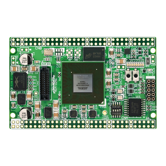
Without proper anti-static handling, you can damage the board. 2. Verify that all components are on the board and appear intact. In typical applications with the Arria II GX FPGA development board, 6G edition, a heat sink is not necessary. However, under extreme conditions or for engineering sample silicon the board might require additional cooling to stay within operating temperature guidelines. -
Page 10: References
2–2 Chapter 2: Getting Started References References Use the following links to check the Altera website for other related information: ■ For the latest board design files and reference designs, refer to the Arria II GX FPGA Development Kit, 6G Edition page. -
Page 11: Introduction
MegaCore IP Library. The Quartus II software (including SOPC Builder) and the Nios II EDS are the primary FPGA development tools used to create the reference designs in this kit. To install the Altera development tools, perform the following steps: 1. -
Page 12: Installing The Arria Ii Gx Fpga Development Kit, 6G Edition
/all at a command prompt to determine the NIC ID. Your NIC ID is the 12- digit hexadecimal number on the Physical Address line. 4. When licensing is complete, Altera emails a license.dat file to you. Store the file on your computer and use the License Setup page of the Options dialog box in the Quartus_II software to enable the software. -
Page 13: Installing The Usb-Blaster Driver
Contains the kit documentation. examples Contains the sample design files for the Arria II GX FPGA Development Kit, 6G Edition. Contains the original data programmed onto the board before shipment. Use this data to restore factory_recovery the board with its original factory contents. - Page 14 3–4 Chapter 3: Software Installation Installing the USB-Blaster Driver Arria II GX FPGA Development Kit, 6G Edition User Guide July 2010 Altera Corporation...
-
Page 15: Introduction
4. Development Board Setup Introduction The instructions in this chapter explain how to set up the Arria II GX FPGA development board, 6G edition. Setting Up the Board To prepare and apply power to the board, perform the following steps: 1. -
Page 16: Factory Default Switch Settings
Chapter 4: Development Board Setup Factory Default Switch Settings Factory Default Switch Settings This section shows the factory switch settings for the Arria II GX FPGA development board, 6G edition. Figure 4–1 shows the switch locations and the default position of each switch on the top side of the board. - Page 17 HSMA DIS Installing the shunt removes HSMC port A from the JTAG chain. Installed ■ Removing the shunt includes HSMC port A in the JTAG chain. ■ July 2010 Altera Corporation Arria II GX FPGA Development Kit, 6G Edition User Guide...
- Page 18 Removing the shunt includes the PCIe device in the JTAG chain. ■ For more information about the FPGA board settings, refer to the Arria II GX FPGA Development Board, 6G Edition Reference Manual. Arria II GX FPGA Development Kit, 6G Edition User Guide July 2010 Altera Corporation...
-
Page 19: Introduction
5. Board Update Portal Introduction The Arria II GX FPGA Development Kit, 6G Edition ships with the Board Update Portal design example stored in the factory portion of the flash memory on the board. The design consists of a Nios II embedded processor, an Ethernet MAC, and an HTML web server. -
Page 20: Using The Board Update Portal To Update User Designs
Chapter 5: Board Update Portal Using the Board Update Portal to Update User Designs 5. Click Arria II GX FPGA Development Kit, 6G Edition on the Board Update Portal web page to access the kit’s home page. Visit this page occasionally for documentation updates and additional new designs. -
Page 21: Introduction
Introduction The kit includes a design example and application called the Board Test System to test the functionality of the Arria II GX FPGA development board, 6G edition. The application provides an easy-to-use interface to alter functional settings and observe the results. - Page 22 Because the application communicates over the JTAG bus to the MAX II device, you can measure the power of any design in the FPGA, including your own designs. Arria II GX FPGA Development Kit, 6G Edition User Guide July 2010 Altera Corporation...
-
Page 23: Preparing The Board
BoardTestSystem.exe application. On Windows, click Start > All Programs > Altera > Arria II GX FPGA Development Kit, 6G Edition <version> > Board Test System to run the application. A GUI appears, displaying the application tab that corresponds to the design running in the FPGA. -
Page 24: Using The Board Test System
The following sections describe the controls on the Config tab. Board Information The Board information controls display static information about your board. Arria II GX FPGA Development Kit, 6G Edition User Guide July 2010 Altera Corporation... -
Page 25: Max Ii Registers
1 = 125 MHz ■ Read / Write Register 2 (OCR2) 2 = 150 MHz ■ 3 = 156.25 MHz ■ You cannot change OCR2 from the GUI. July 2010 Altera Corporation Arria II GX FPGA Development Kit, 6G Edition User Guide... -
Page 26: Jtag Chain Devices
Uninstalling the shunt jumper from jumper J9 pins 1-2 includes the MAX II device in the JTAG chain. Flash Memory Map The Flash memory map control shows the memory map of the flash memory device on your board. Arria II GX FPGA Development Kit, 6G Edition User Guide July 2010 Altera Corporation... -
Page 27: The Gpio Tab
The read-only User DIP switches control displays the current positions of the switches in the user DIP switch bank (SW3). Change the switches on the board to see the graphical display change accordingly. July 2010 Altera Corporation Arria II GX FPGA Development Kit, 6G Edition User Guide... -
Page 28: User Leds
The SRAM&Flash tab allows you to read and write SRAM and flash memory on your board. Figure 6–4 shows the SRAM&Flash tab. Figure 6–4. The SRAM&Flash Tab The following sections describe the controls on the SRAM&Flash tab. Arria II GX FPGA Development Kit, 6G Edition User Guide July 2010 Altera Corporation... -
Page 29: Sram
0x03FE.0000 to 0x003F.FFFF (which corresponds to the unused flash memory address range shown in Figure 6–1 on page 6–2 Table A–1 on page A–1). July 2010 Altera Corporation Arria II GX FPGA Development Kit, 6G Edition User Guide... -
Page 30: The Ddr3 Tab
The Start control initiates DDR3 memory transaction performance analysis. Stop The Stop control terminates transaction performance analysis. Performance Indicators These controls display current transaction performance analysis information collected since you last pressed Start: Arria II GX FPGA Development Kit, 6G Edition User Guide July 2010 Altera Corporation... -
Page 31: Error Control
■ Write then read—Selects read and write transactions for analysis. ■ Read only—Selects read transactions for analysis. ■ Write only—Selects write transactions for analysis. July 2010 Altera Corporation Arria II GX FPGA Development Kit, 6G Edition User Guide... -
Page 32: The Ddr2 Tab
The Start control initiates DDR2 memory transaction performance analysis. Stop The Stop control terminates transaction performance analysis. Performance Indicators These controls display current transaction performance analysis information collected since you last clicked Start: Arria II GX FPGA Development Kit, 6G Edition User Guide July 2010 Altera Corporation... -
Page 33: Error Control
■ Write/Read—Selects read and write transactions for analysis. ■ Read Only—Selects read transactions for analysis. ■ Write Only—Selects write transactions for analysis. July 2010 Altera Corporation Arria II GX FPGA Development Kit, 6G Edition User Guide... -
Page 34: The Hsmc Tab
■ Pattern sync—Shows the pattern synced or not synced state. The pattern is considered synced when the start of the data sequence is detected. Arria II GX FPGA Development Kit, 6G Edition User Guide July 2010 Altera Corporation... -
Page 35: Data Type
Start: ■ TX and RX performance bars—Show the percentage of maximum theoretical data rate that the requested transactions are able to achieve. July 2010 Altera Corporation Arria II GX FPGA Development Kit, 6G Edition User Guide... -
Page 36: The Power Monitor
<install dir>\kits\arriaIIGX_2agx260_fpga\examples\board_test_system directory. On Windows, click Start > All Programs > Altera > Arria II GX FPGA Development Kit, 6G Edition <version> > Power Monitor to start the application. Arria II GX FPGA Development Kit, 6G Edition User Guide... -
Page 37: General Information
The Power Monitor communicates with the MAX II device on the board through the JTAG bus. A power monitor circuit attached to the MAX II device allows you to measure the power that the Arria II GX FPGA device is consuming regardless of the design currently running. -
Page 38: Power Information
The first measurement is Vsense and the difference between the two measurements is Vdif. Plug the values into the equation to determine the power consumption. Arria II GX FPGA Development Kit, 6G Edition User Guide July 2010 Altera Corporation... -
Page 39: Configuring The Fpga Using The Quartus Ii Programmer
FPGA development board, 6G edition, power to the board is on, and no other applications that use the JTAG chain are running. To configure the Arria II GX FPGA, perform the following steps: 1. Start the Quartus II Programmer. - Page 40 6–20 Chapter 6: Board Test System Configuring the FPGA Using the Quartus II Programmer Arria II GX FPGA Development Kit, 6G Edition User Guide July 2010 Altera Corporation...
-
Page 41: Introduction
Nios II EDS tools involved with reprogramming the user portions of the flash memory device. The Arria II GX FPGA development board, 6G edition ships with the CFI flash device preprogrammed with a default factory FPGA configuration for running the Board Update Portal design example and a default user configuration for running the Board Test System demonstration. -
Page 42: Preparing Design Files For Flash Programming
If you have an FPGA design developed using the Quartus II software, and software developed using the Nios II EDS, follow these instructions: 1. On the Windows Start menu, click All Programs > Altera > Nios II EDS > Nios II Command Shell. -
Page 43: Programming Flash Memory Using The Board Update Portal
LEDs (D7-D10) illuminate indicating that the flash device is ready for programming. 8. On the Windows Start menu, click All Programs > Altera > Nios II EDS > Nios II Command Shell. 9. In the Nios II command shell, navigate to the <install dir>\kits\arriaIIGX_2agx260_fpga\factory_recovery directory (or to the... -
Page 44: Restoring The Flash Device To The Factory Settings
LEDs (D7-D10) illuminate indicating that the flash device is ready for programming. 6. On the Windows Start menu, click All Programs > Altera > Nios II EDS > Nios II Command Shell. 7. In the Nios II command shell, navigate to the <install dir>\kits\arriaIIGX_2agx260_fpga\factory_recovery directory and type the... -
Page 45: Restoring The Max Ii Cpld To The Factory Settings
To ensure that you have the most up-to-date factory restore files and information about this product, refer to the Arria II GX FPGA Development Kit, 6G Edition page of the Altera website. July 2010 Altera Corporation Arria II GX FPGA Development Kit, 6G Edition User Guide... - Page 46 A–6 Chapter : Restoring the MAX II CPLD to the Factory Settings Arria II GX FPGA Development Kit, 6G Edition User Guide July 2010 Altera Corporation...
-
Page 47: Document Revision History
(Software Licensing) Email authorization@altera.com Note to Table: (1) You can also contact your local Altera sales office or sales representative. Typographic Conventions The following table shows the typographic conventions this document uses. Visual Cue Meaning Indicate command names, dialog box titles, dialog box options, and other GUI Bold Type with Initial Capital labels. - Page 48 The envelope links to the Email Subscription Management Center page of the Altera website, where you can sign up to receive update notifications for Altera documents. Arria II GX FPGA Development Kit, 6G Edition User Guide July 2010 Altera Corporation...
- Page 49 Mouser Electronics Authorized Distributor Click to View Pricing, Inventory, Delivery & Lifecycle Information: Intel DK-DEV-2AGX260N...
Need help?
Do you have a question about the Arria II GX FPGA and is the answer not in the manual?
Questions and answers