
Related Manuals for Altera Arria V GX FPGA


Summary of Contents for Altera Arria V GX FPGA
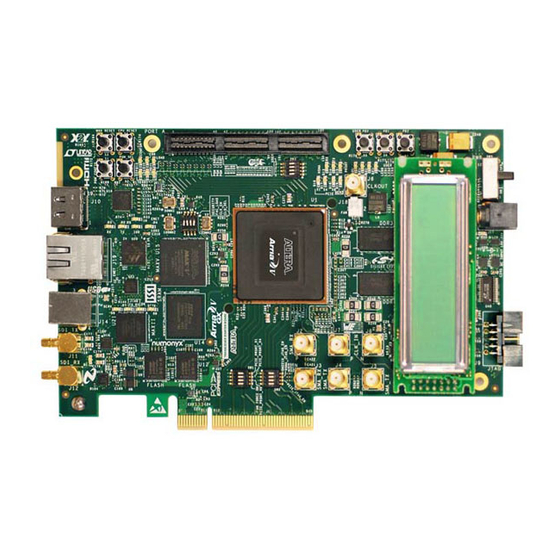
- Page 1 Arria V GX FPGA Development Kit User Guide Arria V GX FPGA Development Kit User Guide 101 Innovation Drive San Jose, CA 95134 www.altera.com UG-01112-1.0 Feedback Subscribe...
- Page 2 © 2012 Altera Corporation. All rights reserved. ALTERA, ARRIA, CYCLONE, HARDCOPY, MAX, MEGACORE, NIOS, QUARTUS and STRATIX words and logos are trademarks of Altera Corporation and registered in the U.S. Patent and Trademark Office and in other countries. All other words and logos identified as trademarks or service marks are the property of their respective holders as described at www.altera.com/common/legal.html.
-
Page 3: Table Of Contents
Arria V GX FPGA Development Kit Installer ........ - Page 4 Calculating Power ..............6–26 Arria V GX FPGA Development Kit...
- Page 5 How to Contact Altera ........
- Page 6 Contents Arria V GX FPGA Development Kit July 2012 Altera Corporation User Guide...
-
Page 7: Chapter 1. About This Kit
The Altera Arria V GX FPGA Development Kit is a complete design environment that includes both the hardware and software you need to develop Arria V GX FPGA designs. Kit Features This section briefly describes the Arria V GX FPGA Development Kit contents. -
Page 8: Arria V Gx Fpga Development Kit Installer
Altera FPGA designs. Arria V GX FPGA Development Kit Installer The license-free Arria V GX FPGA Development Kit installer includes all the documentation and design examples for the kit. For information on installing the Development Kit Installer, refer to “Software... -
Page 9: Chapter 2. Getting Started
Without proper anti-static handling, you can damage the board. 2. Verify that all components on the board appear in place and intact. In typical applications with the Arria V GX FPGA development board, a heat sink is not necessary. However, under extreme conditions or for engineering sample silicon the board might require additional cooling to stay within operating temperature guidelines. -
Page 10: References
2–2 Chapter 2: Getting Started References References Use the following links to check the Altera website for other related information: ■ For the latest board design files and reference designs, refer to the Arria V GX FPGA Development Kit page. -
Page 11: Chapter 3. Software Installation
MegaCore IP Library. The Quartus II software (including SOPC Builder) and the Nios II EDS are the primary FPGA development tools used to create the reference designs in this kit. To install the Altera development tools, perform the following steps: 1. - Page 12 /all at a command prompt to determine the NIC ID. Your NIC ID is the 12- digit hexadecimal number on the Physical Address line. 4. When licensing is complete, Altera emails a license.dat file to you. Store the file on your computer and use the License Setup page of the Options dialog box in the Quartus_II software to enable the software.
-
Page 13: Installing The Arria V Gx Fpga Development Kit
Installing the Arria V GX FPGA Development Kit Installing the Arria V GX FPGA Development Kit To install the Arria V GX FPGA Development Kit, perform the following steps: 1. Download the Arria V GX FPGA Development Kit installer from the... -
Page 14: Installing The Usb-Blaster Ii Driver
Altera website. On the Altera Programming Cable Driver Information page of the Altera website, locate the table entry for your configuration and click the link to access the instructions. For USB-Blaster II configuration details, refer to the On-Board USB-Blaster II page. -
Page 15: Chapter 4. Development Board Setup
4. Development Board Setup The instructions in this chapter explain how to set up the Arria V GX FPGA development board. Setting Up the Board To prepare and apply power to the board, perform the following steps: 1. The Arria V GX FPGA development board ships with its board switches preconfigured to support the design examples in the kit. -
Page 16: Factory Default Switch And Jumper Settings
Chapter 4: Development Board Setup Factory Default Switch and Jumper Settings Factory Default Switch and Jumper Settings This section shows the factory switch and jumper settings for the Arria V GX FPGA development board. Figure 4–1 shows the switch and jumper locations and the default position of each switch and jumper on the top side of the board. - Page 17 FPGA 1 from flash at power up. OFF, (logical 1) = load the user design for Arria V FPGA ■ 1 from flash at power up. Factory2 Switch 4 is for factory test only. July 2012 Altera Corporation Arria V GX FPGA Development Kit User Guide...
- Page 18 Switch 3 has the following options: PCIE_PRSNT2 ON (0) = x8 presence detect is enabled. ■ n_x8 OFF (1) = x8 presence detect is disabled. ■ — — Arria V GX FPGA Development Kit July 2012 Altera Corporation User Guide...
- Page 19 Note: When setting this jumper to 3.3 V, make sure the FMC_VCCPD is on the correct setting (J5 shunt on pins 2-3). FAN2 Powers the fan for FPGA 2 Installed July 2012 Altera Corporation Arria V GX FPGA Development Kit User Guide...
- Page 20 Note: FMC is not available for rev. A boards. FAN1 Powers the fan for FPGA 1 Installed For more information about the FPGA board settings, refer to the Arria V GX FPGA Development Board Reference Manual. Arria V GX FPGA Development Kit July 2012 Altera Corporation User Guide...
-
Page 21: Chapter 5. Board Update Portal
5. Board Update Portal The Arria V GX FPGA Development Kit ships with the Board Update Portal design example stored in the factory portion of the flash memory on the board. The design consists of a Nios II embedded processor, an Ethernet MAC, and an HTML web server. -
Page 22: Using The Board Update Portal To Update User Designs
IP address from the LCD into the browser address bar. The Board Update Portal web page appears in the browser. You can click Arria V GX FPGA Development Kit on the Board Update Portal web page to access the kit’s home page for documentation updates and additional new designs. -
Page 23: Chapter 6. Board Test System
6. Board Test System The kit includes a design example and an application called the Board Test System to test the functionality of the Arria V GX FPGA development board and supported daughtercards. The application provides an easy-to-use interface to alter functional settings and observe the results. -
Page 24: Preparing The Board
4. Set the Load Selector (SW5.3) to the off (user) position. For more information about the board’s DIP switch and jumper settings, refer to the Arria V GX FPGA Development Board Reference Manual. 5. Turn on the power to the board. The board loads the design stored in the user hardware 1 portion of flash memory into the FPGA. -
Page 25: Running The Board Test System
BoardTestSystem.exe application. On Windows, click Start > All Programs > Altera > Arria V GX FPGA Development Kit <version> > Board Test System to run the application. A GUI appears, displaying the application tab that corresponds to the design running in the FPGA. -
Page 26: The System Info Tab
■ The MAX II code resides in the <install dir>\kits\arriaVGX_5agxfb3hf40es_fpga\examples directory. Newer revisions of this code might be available on the Arria V GX FPGA Development Kit page of the Altera website. ■ MAC—Indicates the MAC address of the board. -
Page 27: Jtag Chain
If you plug in an external USB-Blaster cable to the JTAG header (J1), the On-Board USB-Blaster II is disabled. For details on the JTAG chain, refer to the Arria V GX FPGA Development Board Reference Manual. For USB-Blaster II configuration details, refer to the... -
Page 28: Qsys Memory Map
The Character LCD controls allow you to display text strings on the character LCD on your board. Type text in the text boxes and then click Display. Click Read to read the currently shown on the LCD display. Arria V GX FPGA Development Kit July 2012 Altera Corporation User Guide... -
Page 29: User Dip Switch
The read-only Push button switches control displays the current state of the board user push buttons. Press a push button on the board to see the graphical display change accordingly. July 2012 Altera Corporation Arria V GX FPGA Development Kit User Guide... -
Page 30: The Flash Tab
0x0800.0000. Valid are entries are 0x0000.0000 through 0x07FF.FFFF. If you enter an address outside of the flash memory address space, a warning message identifies the valid flash memory address range. Arria V GX FPGA Development Kit July 2012 Altera Corporation User Guide... -
Page 31: Write
Erases flash memory, which is limited to a scratch page in the upper 128K block. Flash Memory Map Displays the flash memory map for the Arria V GX FPGA Development Kit. July 2012 Altera Corporation Arria V GX FPGA Development Kit... -
Page 32: The Hsma Tab
■ Pattern sync—Shows the pattern synced or not synced state. The pattern is considered synced when the start of the data sequence is detected. Arria V GX FPGA Development Kit July 2012 Altera Corporation User Guide... -
Page 33: Port
LF —lowest frequency divide by 33 data pattern ■ Settings HF1, HF2, HF3, LF are for transmit observation only and are not used in the receiver data detection circuitry. July 2012 Altera Corporation Arria V GX FPGA Development Kit User Guide... -
Page 34: Error Control
TX and RX performance bars—Show the percentage of maximum theoretical data rate that the requested transactions are able to achieve. Tx (MBps) and Rx (MBps)—Show the number of bytes of data analyzed per ■ second. Arria V GX FPGA Development Kit July 2012 Altera Corporation User Guide... -
Page 35: The Sfp/Sma/C2C Tab
Pattern sync—Shows the pattern synced or not synced state. The pattern is ■ considered synced when the start of the data sequence is detected. July 2012 Altera Corporation Arria V GX FPGA Development Kit User Guide... -
Page 36: Port
HF1—highest frequency divide-by-2 data pattern "10101010" HF2—next highest frequency divide-by-6 data pattern "111000111000" ■ HF3—second lowest frequency divide-by-22 data pattern ■ ■ LF —lowest frequency divide by 33 data pattern Arria V GX FPGA Development Kit July 2012 Altera Corporation User Guide... -
Page 37: Error Control
TX and RX performance bars—Show the percentage of maximum theoretical data rate that the requested transactions are able to achieve. ■ Tx (MBps) and Rx (MBps)—Show the number of bytes of data analyzed per second. July 2012 Altera Corporation Arria V GX FPGA Development Kit User Guide... -
Page 38: The Hsmb/Fmc Tab
Pattern sync—Shows the pattern synced or not synced state. The pattern is ■ considered synced when the start of the data sequence is detected. Arria V GX FPGA Development Kit July 2012 Altera Corporation User Guide... -
Page 39: Port
HF1—highest frequency divide-by-2 data pattern "10101010" ■ HF2—next highest frequency divide-by-6 data pattern "111000111000" ■ ■ HF3—second lowest frequency divide-by-22 data pattern ■ LF —lowest frequency divide by 33 data pattern July 2012 Altera Corporation Arria V GX FPGA Development Kit User Guide... -
Page 40: Error Control
TX and RX performance bars—Show the percentage of maximum theoretical data rate that the requested transactions are able to achieve. ■ Tx (MBps) and Rx (MBps)—Show the number of bytes of data analyzed per second. Arria V GX FPGA Development Kit July 2012 Altera Corporation User Guide... -
Page 41: The Sdi/Bullseye Tab
Pattern sync—Shows the pattern synced or not synced state. The pattern is ■ considered synced when the start of the data sequence is detected. July 2012 Altera Corporation Arria V GX FPGA Development Kit User Guide... -
Page 42: Port
LF —lowest frequency divide by 33 data pattern ■ Settings HF1, HF2, HF3, LF are for transmit observation only and are not used in the receiver data detection circuitry. Arria V GX FPGA Development Kit July 2012 Altera Corporation User Guide... -
Page 43: Error Control
TX and RX performance bars—Show the percentage of maximum theoretical data rate that the requested transactions are able to achieve. Tx (MBps) and Rx (MBps)—Show the number of bytes of data analyzed per ■ second. July 2012 Altera Corporation Arria V GX FPGA Development Kit User Guide... -
Page 44: The Sma Tab
Pattern sync—Shows the pattern synced or not synced state. The pattern is ■ considered synced when the start of the data sequence is detected. Arria V GX FPGA Development Kit July 2012 Altera Corporation User Guide... -
Page 45: Port
LF —lowest frequency divide by 33 data pattern ■ Settings HF1, HF2, HF3, LF are for transmit observation only and are not used in the receiver data detection circuitry. July 2012 Altera Corporation Arria V GX FPGA Development Kit User Guide... -
Page 46: Error Control
You can also run the Power Monitor as a stand-alone application. PowerMonitor.exe resides in the <install dir>\kits\arriaVGX_5agxfb3hf40es_fpga\examples\board_test_system directory. On Windows, click Start > All Programs > Altera > Arria V GX FPGA Development Kit <version> > Power Monitor to start the application. Arria V GX FPGA Development Kit... -
Page 47: General Information
The Power Monitor communicates with the MAX II device on the board through the JTAG bus. A power monitor circuit attached to the MAX II device allows you to measure the power that the Arria V GX FPGA is consuming. Figure 6–10 shows the Power Monitor. -
Page 48: Power Information
(the side opposite the power source) and then measure the voltage on the other side. The first measurement is Vsense and the difference between the two measurements is Vdif. Plug the values into the equation to determine the power consumption. Arria V GX FPGA Development Kit July 2012 Altera Corporation User Guide... -
Page 49: The Clock Control
<install dir>\kits\arriaVGX_5agxfb3hf40es_fpga\examples\board_test_system directory. On Windows, click Start > All Programs > Altera > Arria V GX FPGA Development Kit <version> > Clock Control to start the application. For more information about the Si570, Si571, and Si5338A and the Arria V GX FPGA development board’s clocking circuitry and clock input pins, refer to the... -
Page 50: Registers
FPGA development board, power to the board is on, and no other applications that use the JTAG chain are running. To configure the Arria V GX FPGA, perform the following steps: 1. Start the Quartus II Programmer. 2. Click Auto Detect to display the devices in the JTAG chain. -
Page 51: Samtec High-Speed Bull's Eye Connector
For details on the pinout, refer to the Arria V GX FPGA Development Board Reference Manual. For details on how to use the Bull’s Eye interface, refer to the Altera Arria V GX platforms page on the Samtec website (www.samtec.com). - Page 52 6–30 Chapter 6: Board Test System Samtec High-speed Bull’s Eye Connector Arria V GX FPGA Development Kit July 2012 Altera Corporation User Guide...
-
Page 53: Cfi Flash Memory Map
A. Programming the Flash Memory Device As you develop your own project using the Altera tools, you can program the flash memory device so that your own design loads from flash memory into the FPGA on power up. This appendix describes the preprogrammed contents of the common flash... -
Page 54: Preparing Design Files For Flash Programming
If you have an FPGA design developed using the Quartus II software, and software developed using the Nios II EDS, follow these instructions: 1. On the Windows Start menu, click All Programs > Altera > Nios II EDS > Nios II Command Shell. -
Page 55: Programming Flash Memory Using The Nios Ii Eds
100%. The flash device is ready for programming. 8. On the Windows Start menu, click All Programs > Altera > Nios II EDS > Nios II Command Shell. 9. In the Nios II command shell, navigate to the <install dir>\kits\arriaVGX_5agxfb3hf40es_fpga\factory_recovery directory (or to the... - Page 56 100%. The Config Done LED (D16) illuminates indicating that the flash device is ready for programming. 6. On the Windows Start menu, click All Programs > Altera > Nios II EDS > Nios II Command Shell.
-
Page 57: Restoring The Max Ii Cpld To The Factory Settings
Configuration is complete when the progress bar reaches 100%. To ensure that you have the most up-to-date factory restore files and information about this product, refer to the Arria V GX FPGA Development Kit page of the Altera website. July 2012 Altera Corporation... - Page 58 A–6 Appendix A: Programming the Flash Memory Device Restoring the MAX II CPLD to the Factory Settings Arria V GX FPGA Development Kit July 2012 Altera Corporation User Guide...
-
Page 59: Additional Information
(software licensing) Email authorization@altera.com Note to Table: (1) You can also contact your local Altera sales office or sales representative. Typographic Conventions The following table shows the typographic conventions this document uses. Visual Cue Meaning Indicate command names, dialog box titles, dialog box options, and other GUI Bold Type with Initial Capital labels. - Page 60 Email Subscription Management Center page of the Altera website, where you can sign up to receive update notifications for Altera documents. The feedback icon allows you to submit feedback to Altera about the document. Methods for collecting feedback vary as appropriate for each document.
Need help?
Do you have a question about the Arria V GX FPGA and is the answer not in the manual?
Questions and answers