
Related Manuals for Altera Stratix 10 GX FPGA


Summary of Contents for Altera Stratix 10 GX FPGA
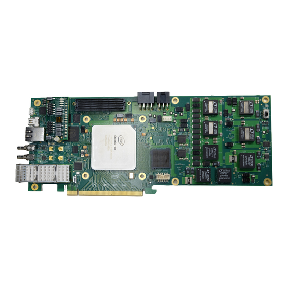
- Page 1 ® ® Intel Stratix 10 GX FPGA Development Kit User Guide Subscribe UG-20046 | 2018.07.20 Send Feedback Latest document on the web: HTML...
-
Page 2: Table Of Contents
Contents Contents 1. Overview........................4 1.1. General Development Board Description..............4 1.2. Recommended Operating Conditions................ 5 1.3. Handling the Board....................5 2. Getting Started....................... 6 2.1. Installing Quartus Prime Software................6 2.1.1. Activating Your License................6 2.2. Development Board Package................... 7 2.3. - Page 3 Contents 6. Board Test System......................65 6.1. Preparing the Board..................... 66 6.2. Running the Board Test System................67 6.3. Using the Board Test System................. 67 6.3.1. The Configure Menu................. 67 6.3.2. The System Info Tab................68 6.3.3. The GPIO Tab..................70 6.3.4.
-
Page 4: Overview
Fingers Power Regulators Intel Corporation. All rights reserved. Intel, the Intel logo, Altera, Arria, Cyclone, Enpirion, MAX, Nios, Quartus and Stratix words and logos are trademarks of Intel Corporation or its subsidiaries in the U.S. and/or other countries. Intel warrants performance of its FPGA and semiconductor products to current specifications in... -
Page 5: Recommended Operating Conditions
1. Overview UG-20046 | 2018.07.20 1.2. Recommended Operating Conditions • Recommended ambient operating temperature range: 0C to 45C • Maximum ICC load current: 100 A • Maximum ICC load transient percentage: 30 % • FPGA maximum power supported by the supplied heatsink/fan: 200 W 1.3. -
Page 6: Getting Started
5. In the Find/Activate Products dialog box, enter your development kit serial number and click Search. Intel Corporation. All rights reserved. Intel, the Intel logo, Altera, Arria, Cyclone, Enpirion, MAX, Nios, Quartus and Stratix words and logos are trademarks of Intel Corporation or its subsidiaries in the U.S. and/or other countries. -
Page 7: Development Board Package
6. When your product appears, turn on the check box next to the product name. 7. Click Activate Selected Products and click Close. 8. When licensing is complete, Altera emails a license.dat file to you. Store the file on your computer and use the License Setup page of the Options dialog box in the Quartus Prime software to enable the software. -
Page 8: Installing The Usb-Blaster Driver
Installation instrcutions for the On-Board Intel FPGA Download Cable II driver for your operating system are available on the Intel website. On the Altera Programming Cable Driver Information web page of the Intel website, locate the table entry for your configuration and click the link to access the instructions. -
Page 9: Development Board Setup
LED illuminates. Intel Corporation. All rights reserved. Intel, the Intel logo, Altera, Arria, Cyclone, Enpirion, MAX, Nios, Quartus and Stratix words and logos are trademarks of Intel Corporation or its subsidiaries in the U.S. and/or other countries. -
Page 10: Default Switch And Jumper Settings
3. Development Board Setup UG-20046 | 2018.07.20 3.2. Default Switch and Jumper Settings This topic shows you how to restore the default factory settings and explains their functions. Figure 3. Default Switch Settings 1. Set DIP switch bank (SW2) to match the following table Table 3. - Page 11 3. Development Board Setup UG-20046 | 2018.07.20 3. Set DIP switch bank (SW6) to match the following table. Table 5. SW6 JTAG Bypass DIP Switch Default Settings (Board Bottom) Switch Board Label Function Default Position Intel Stratix 10 OFF to enable the Intel Stratix 10 in the JTAG chain.
- Page 12 3. Development Board Setup UG-20046 | 2018.07.20 Switch Board Label Function Default Position OFF for setting RZQ resistor of Bank 2M to 240 Ohm ON for setting the SDI SI516_FS frequency to 148.35 REFCLK OFF for setting the SDI frequency to 148.5 REFCLK Table 9.
-
Page 13: Factory Reset
3. Development Board Setup UG-20046 | 2018.07.20 3.3. Factory Reset This section is a part of the Board Test System (BTS) GUI that is under development. It will be updated in a future version when new information is available. ® ®... -
Page 14: Board Components
Stratix 10 FPGA Development Board Image - Rear Intel Corporation. All rights reserved. Intel, the Intel logo, Altera, Arria, Cyclone, Enpirion, MAX, Nios, Quartus and Stratix words and logos are trademarks of Intel Corporation or its subsidiaries in the U.S. and/or other countries. - Page 15 4. Board Components UG-20046 | 2018.07.20 Table 10. Stratix 10 GX FPGA Development Board Components Board Reference Type Description Featured Devices FPGA Stratix 10 GX FPGA, 1SG280LU3F50E3VGS1. • Adaptive logic modules (ALMs): 933,120 • LEs (K): 2,753 • Registers: 3,732,480 •...
- Page 16 4. Board Components UG-20046 | 2018.07.20 Board Reference Type Description Error LED Illuminates when the FPGA configuration fails. This LED resides on the LED daughter board. Power LED Illuminates when the board is powered on. Temperature LED Illuminates when an over temperature condition occurs for the FPGA device.
- Page 17 4. Board Components UG-20046 | 2018.07.20 Board Reference Type Description PCIe x16 gold fingers PCIe TX/RX x16 interface from FPGA bank 1C, 1D and 1E. Mini Display Port Video Connector Four TX channels of Display Port Video interface from FPGA Bank 1F.
- Page 18 4. Board Components UG-20046 | 2018.07.20 Board Reference Type Description connected to the 6-pin Aux PCIe power connector provided by the PC system along with J27, or else the board will not power on. Power switch Switch to power ON or OFF the board when supplied from the DC input jack.
-
Page 19: Max V Cpld System Controller
4. Board Components UG-20046 | 2018.07.20 4.2. MAX V CPLD System Controller The development board utilizes the EPM2210 System Controller, an Intel MAX V CPLD for the following purposes: • FPGA configuration from flash memory • Power consumption monitoring • Temperature monitoring •... - Page 20 4. Board Components UG-20046 | 2018.07.20 Schematic Signal Name Pin Number I/O Standard Description 1.8V MAX V to Intel MAX 10 Intel USB_CFG1 FPGA Download Cable bus 1.8V MAX V to Intel MAX 10 Intel USB_CFG13 FPGA Download Cable bus 1.8V MAX V to Intel MAX 10 Intel USB_CFG14...
- Page 21 4. Board Components UG-20046 | 2018.07.20 Schematic Signal Name Pin Number I/O Standard Description 1.8V Partial reconfiguration FPGA_PR_REQUEST request signal 1.8V Flash address bus FLASH_ADDR1 1.8V Flash address bus FLASH_ADDR2 1.8V Flash address bus FLASH_ADDR3 1.8V Flash address bus FLASH_ADDR4 1.8V Flash address bus FLASH_ADDR5...
- Page 22 4. Board Components UG-20046 | 2018.07.20 Schematic Signal Name Pin Number I/O Standard Description 1.8V Flash data bus FLASH_DATA4 1.8V Flash data bus FLASH_DATA5 1.8V Flash data bus FLASH_DATA6 1.8V Flash data bus FLASH_DATA7 1.8V Flash data bus FLASH_DATA8 1.8V Flash data bus FLASH_DATA9 1.8V...
- Page 23 4. Board Components UG-20046 | 2018.07.20 Schematic Signal Name Pin Number I/O Standard Description 1.8V FPGA configuration data bus FPGA_CONFIG_D11 1.8V FPGA configuration data bus FPGA_CONFIG_D12 1.8V FPGA configuration data bus FPGA_CONFIG_D13 1.8V FPGA configuration data bus FPGA_CONFIG_D14 1.8V FPGA configuration data bus FPGA_CONFIG_D15 1.8V MAX V output enable...
-
Page 24: Fpga Configuration
4. Board Components UG-20046 | 2018.07.20 4.3. FPGA Configuration You can use the Quartus Programmer to configure the FPGA with your SRAM Object File (.sof). Ensure the following: • The Quartus Programmer and the Intel FPGA Download Cable II driver are installed on the host computer. - Page 25 4. Board Components UG-20046 | 2018.07.20 Figure 7. JTAG Chain Conceptual Block Diagram External JTAG Header from LED Daughter Board External JTAG S10_JTAG Intel Stratix 10 FPGA (U1) MAX 10 M5_JTAG MAX V System Intel FPGA Download Cable II Controller (U11) (U23) FMCA_JTAG FMCA...
-
Page 26: Status Elements
4. Board Components UG-20046 | 2018.07.20 4.4. Status Elements The Intel Stratix 10 GX FPGA development board includes status LEDs as listed below. Table 12. Board-Specific Status LEDs Board Reference Schematic Signal Name I/O Standard D3 on the LED board 2.5V... -
Page 27: User Input-Output Components
MAX_RESETn 4.5.2. User-Defined DIP Switches The Intel Stratix 10 GX FPGA development board includes a set of four pin DIP switch. There are no board-specific functions for these switches. When the switch is in the OFF position, logic 1 is selected. When the switch is in the ON position, logic 0 is selected. - Page 28 4. Board Components UG-20046 | 2018.07.20 Board Reference Schematic Signal Name FPGA Pin Number I/O Standard D10 on LED board 1.8V USER_LED_G3 D4 on LED board 1.8V USER_LED_R0 D7 on LED board 1.8V USER_LED_R1 D9 on LED board 1.8V USER_LED_R2 D10 on LED board 1.8V USER_LED_R3...
-
Page 29: Components And Interfaces
Intel Stratix 10 GX FPGA device. 4.6.1. PCI Express The Intel Stratix 10 GX FPGA development board is designed to fit entirely into a PC motherboard with a x16 PCI Express slot that can accommodate a full height, 3-slot long form factor add-in card. - Page 30 4. Board Components UG-20046 | 2018.07.20 Receive bus Schematic Signal FPGA Pin Number I/O Standard Description Name – – Link with DIP switch PCIE_PRSNT1n (SW2) – – Link with DIP switch PCIE_PRSNT2n_X1 (SW2) – – Link with DIP switch PCIE_PRSNT2n_X4 (SW2) –...
- Page 31 4. Board Components UG-20046 | 2018.07.20 Receive bus Schematic Signal FPGA Pin Number I/O Standard Description Name AY49 1.4 V PCML Receive bus PCIE_RX_P10 AU47 1.4 V PCML Receive bus PCIE_RX_P11 AR43 1.4 V PCML Receive bus PCIE_RX_P12 AT45 1.4 V PCML Receive bus PCIE_RX_P13 AP45...
-
Page 32: 10/100/1000 Ethernet Phy
MegaCore MAC function. The PHY-to-MAC interface employs SGMII using the Intel Stratix 10 GX FPGA LVDS pins in Soft-CDR mode at 1.25 Gbps trasmit and receive. In 10 Mb or 100 Mb mode, the SGMII interface still runs at 1.25 GHz but the packet data is repeated 10 or 100 times. -
Page 33: Hilo External Memory Interface
MDI_P3 interface 4.6.3. HiLo External Memory Interface This section describes the Intel Stratix 10 GX FPGA development board's external memory interface support and also their signal names, types and connectivity relative to the Intel Stratix 10 GX FPGA. The HiLo connector supports plugins for the following memory interfaces: •... - Page 34 4. Board Components UG-20046 | 2018.07.20 Board Reference - HiLo Pin HiLo Schematic Signal FPGA Pin Number I/O Standard Number Name Adjustable MEM_ADDR_CMD4 Adjustable MEM_ADDR_CMD5 Adjustable MEM_ADDR_CMD6 Adjustable MEM_ADDR_CMD7 Adjustable MEM_ADDR_CMD8 Adjustable MEM_ADDR_CMD9 Adjustable MEM_ADDR_CMD10 Adjustable MEM_ADDR_CMD11 Adjustable MEM_ADDR_CMD12 Adjustable MEM_ADDR_CMD13 Adjustable MEM_ADDR_CMD14...
- Page 35 4. Board Components UG-20046 | 2018.07.20 Board Reference - HiLo Pin HiLo Schematic Signal FPGA Pin Number I/O Standard Number Name Adjustable MEM_DMB0 Adjustable MEM_DMB1 Adjustable MEM_DMB2 Adjustable MEM_DMB3 Adjustable MEM_DQ_ADDR_CMD0 Adjustable MEM_DQ_ADDR_CMD1 Adjustable MEM_DQ_ADDR_CMD2 Adjustable MEM_DQ_ADDR_CMD3 Adjustable MEM_DQ_ADDR_CMD4 Adjustable MEM_DQ_ADDR_CMD5 Adjustable MEM_DQ_ADDR_CMD6...
- Page 36 4. Board Components UG-20046 | 2018.07.20 Board Reference - HiLo Pin HiLo Schematic Signal FPGA Pin Number I/O Standard Number Name Adjustable MEM_DQA21 Adjustable MEM_DQA22 Adjustable MEM_DQA23 Adjustable MEM_DQA24 Adjustable MEM_DQA25 Adjustable MEM_DQA26 Adjustable MEM_DQA27 Adjustable MEM_DQA28 Adjustable MEM_DQA29 Adjustable MEM_DQA30 Adjustable MEM_DQA31...
- Page 37 4. Board Components UG-20046 | 2018.07.20 Board Reference - HiLo Pin HiLo Schematic Signal FPGA Pin Number I/O Standard Number Name Adjustable MEM_DQB21 Adjustable MEM_DQB22 Adjustable MEM_DQB23 Adjustable MEM_DQB24 Adjustable MEM_DQB25 Adjustable MEM_DQB26 Adjustable MEM_DQB27 Adjustable MEM_DQB28 Adjustable MEM_DQB29 Adjustable MEM_DQB30 Adjustable MEM_DQB31...
-
Page 38: Fmc
Adjustable MEM_QKB_P1 4.6.4. FMC The Intel Stratix 10 GX FPGA development board includes a high pin count (HPC) FPGA mezzanine card (FMC) connector that functions with a quadrature amplitude modulation (QAM) digital-to-analog converter (DAC) FMC module or daughtercard. This pin-out satisfies a QAM DAC that requires 58 low-voltage differential signaling (LVDS) data output pairs, one LVDS input clock pair and three low-voltage LVDS control pairs from the FPGA device. - Page 39 4. Board Components UG-20046 | 2018.07.20 Board Reference Schematic Signal Name FPGA Pin Number I/O Standard 1.4V PCML FMCA_DP_C2M_P0 1.4V PCML FMCA_DP_C2M_P1 1.4V PCML FMCA_DP_C2M_P2 1.4V PCML FMCA_DP_C2M_P3 1.4V PCML FMCA_DP_C2M_P4 1.4V PCML FMCA_DP_C2M_P5 1.4V PCML FMCA_DP_C2M_P6 1.4V PCML FMCA_DP_C2M_P7 1.4V PCML FMCA_DP_C2M_P8 1.4V PCML...
- Page 40 4. Board Components UG-20046 | 2018.07.20 Board Reference Schematic Signal Name FPGA Pin Number I/O Standard 1.4V PCML FMCA_DP_M2C_P2 1.4V PCML FMCA_DP_M2C_P3 1.4V PCML FMCA_DP_M2C_P4 1.4V PCML FMCA_DP_M2C_P5 1.4V PCML FMCA_DP_M2C_P6 1.4V PCML FMCA_DP_M2C_P7 1.4V PCML FMCA_DP_M2C_P8 1.4V PCML FMCA_DP_M2C_P9 1.4V PCML FMCA_DP_M2C_P10 1.4V PCML...
- Page 41 4. Board Components UG-20046 | 2018.07.20 Board Reference Schematic Signal Name FPGA Pin Number I/O Standard BA19 LVDS FMCA_LA_RX_N5 AR16 LVDS FMCA_LA_RX_N6 BF19 LVDS FMCA_LA_RX_N7 AT16 LVDS FMCA_LA_RX_N8 AT14 LVDS FMCA_LA_RX_N9 AU14 LVDS FMCA_LA_RX_N10 BJ18 LVDS FMCA_LA_RX_N11 AU13 LVDS FMCA_LA_RX_N12 AY13 LVDS FMCA_LA_RX_N13...
- Page 42 4. Board Components UG-20046 | 2018.07.20 Board Reference Schematic Signal Name FPGA Pin Number I/O Standard BA11 LVDS FMCA_LA_TX_N9 BB12 LVDS FMCA_LA_TX_N10 BF17 LVDS FMCA_LA_TX_N11 BB10 LVDS FMCA_LA_TX_N12 BH17 LVDS FMCA_LA_TX_N13 BC11 LVDS FMCA_LA_TX_N14 BD10 LVDS FMCA_LA_TX_N15 BF10 LVDS FMCA_LA_TX_N16 AP13 LVDS FMCA_LA_TX_P0...
-
Page 43: Qsfp
4. Board Components UG-20046 | 2018.07.20 4.6.5. QSFP The Intel Stratix 10 GX FPGA development board includes a Quad Small Form-Factor Pluggable (QSFP) module. Table 20. QSFP Pin Assignments Board Reference Schematic Signal FPGA Pin Number I/O Standard Description Name BE26 1.8V... -
Page 44: I 2 C
4. Board Components UG-20046 | 2018.07.20 4.6.6. I C supports communication between integrated circuits on a board. It is a simple two-wire bus that consists of a serial data line (SDA) and a serial clock (SCL). The MAX V and the Intel Stratix 10 devices use the I C for reading and writing to the various components on the board such as programmable clock generators, VID regulators, ADC and temperature sensors. -
Page 45: Displayport
BH20 1.8V Dedicated I C to FMC FMCA_SDA Connector 4.6.7. DisplayPort The Intel Stratix 10 GX FPGA development board includes a Mini-DisplayPort connector. Table 26. Mini-DisplayPort Schematic Signal Names and Functions Board Reference Schematic Signal FPGA Pin Number I/O Standard... -
Page 46: Sdi Video Input/Output Ports
DP_ML_LANE_CP3 4.6.8. SDI Video Input/Output Ports The Intel Stratix 10 GX FPGA development board includes a SDI port, which consists of a M23428G-33 cable driver and a M23544G-14 cable equalizer. The PHY devices from Macom interface to single-ended HDBNC connectors. - Page 47 4. Board Components UG-20046 | 2018.07.20 Table 29. SDI Cable Equalizer Lengths Cable Type Data Rate (Mbps) Maximum Cable Length (m) Belden 1694A Belden 1694A 1485 Belden 1694A 2970 Table 30. SDI Video Input Interface Pin Assignments, Schematic Signal Names and Functions Board Reference Schematic Signal Name...
-
Page 48: Clock Circuits
4. Board Components UG-20046 | 2018.07.20 4.7. Clock Circuits 4.7.1. On-Board Oscillators Figure 10. Stratix 10 GX FPGA Board - Clock Inputs and Default Frequencies REFCLK1 (155.52 MHz LVDS) OUT0 REFCLK_QSFPI1 (644.53125 MHz LVDS) OUT1 REFCLK_DP (135 MHz LVDS) OUT2... -
Page 49: Off-Board Clock I/O
4. Board Components UG-20046 | 2018.07.20 Source Schematic Signal Frequency I/O Standard Stratix 10 FPGA Application Name Pin Number LVDS BA22 FPGA FPGA_OSC_CLK1 125 MHz configuration clock LVDS – 125 MHz MAX V clock MAXV_OSC_CLK1 LVDS – 125 MHz MAX V clock CLK_CONFIG 50 MHz 1.8V LVCMOS... -
Page 50: Memory
FPGA. 4.8.1. Flash The Intel Stratix 10 GX FPGA development board supports two 1 Gb CFI-compatible synchronous flash devices for non-volatile storage of FPGA configuration data, board information, test application data and user code space. These devices are part of the shared bus that connects to the flash memory, FPGA and MAX V CPLD EPM2210 System Controller. - Page 51 4. Board Components UG-20046 | 2018.07.20 Board Reference Schematic Signal FPGA Pin Number I/O Standard Description Name BJ28 1.8V Ready FLASH_RDYBSYN1 BG30 1.8V Reset FLASH_RESETN BH28 1.8V Write Enable FLASH_WEN – 1.8V Write protect FLASH_WPN AU28 1.8V Address bus FLASH_ADDR1 AU29 1.8V Address bus...
-
Page 52: Programming Flash Using Quartus Programmer
4. Board Components UG-20046 | 2018.07.20 Board Reference Schematic Signal FPGA Pin Number I/O Standard Description Name BB34 1.8V Data bus FLASH_DATA4 BB33 1.8V Data bus FLASH_DATA5 BD35 1.8V Data bus FLASH_DATA6 BD34 1.8V Data bus FLASH_DATA7 BC33 1.8V Data bus FLASH_DATA8 BD33 1.8V... - Page 53 4. Board Components UG-20046 | 2018.07.20 Attention: Using the Quartus Programmer to program a device on the board causes other JTAG- based applications such as the Board Test System and the Power Monitor to lose their connection to the board. Restart those applications after programming is complete. ®...
-
Page 54: Daughtercards
4. Board Components UG-20046 | 2018.07.20 4.9. Daughtercards The Intel Stratix 10 GX FPGA development kit provides a full-featured hardware development platform for prototyping and testing high-speed interfaces to a Intel Stratix 10 GX FPGA. Table 37. Stratix 10 FPGA Development Kit Daughtercards... - Page 55 4. Board Components UG-20046 | 2018.07.20 4.9.1.2. DDR4 Figure 12. DDR4 Block Diagram EMIF Byte 8 Byte 6-7 Byte 4-5 Byte 2-3 Byte 0-1 Connector DDR4 SDRAM DDR4 SDRAM DDR4 SDRAM DDR4 SDRAM DDR4 SDRAM DDR4 x 72 VDD/2.5 V 4.9.1.3.
- Page 56 4. Board Components UG-20046 | 2018.07.20 4.9.1.4. QDR-IV QDR-IV x 36 SRAM devices enable you to maximize bandwidth with separate read and write ports. Figure 14. QDR-IV Block Diagram HILO CONNECTOR QDR IV x 36 VDD_V1P3 QDRIV_ODT_A0-A24 A0-A24 A0-A24 QDRIV_ODT_ANIV ANIV ANIV QDRIV_ODT_ANIV...
- Page 57 4. Board Components UG-20046 | 2018.07.20 Figure 15. Stratix 10 FPGA Development Kit FMC Block Diagram FMCA Port FMCA Stratix 10 FPGA The following table shows the complete signal connections assigned for Intel FMC interface at the FMCA port. Table 38. FMCA Connector (J13) Signal Assignments Number VREF_F...
- Page 58 4. Board Components UG-20046 | 2018.07.20 Number FMCA_D FMCA_L FMCA_L FMCA_D P_M2C_ A_TX_N A_RX_C P_M2C_ LK_P1 FMCA_L FMCA_L FMCA_D A_RX_P A_RX_C P_M2C_ LK_N1 FMCA_D FMCA_L FMCA_L FMCA_L FMCA_D P_M2C_ A_TX_P A_RX_N A_RX_P P_M2C_ FMCA_D FMCA_L FMCA_L FMCA_L FMCA_D P_M2C_ A_TX_N A_TX_P A_RX_N P_M2C_...
- Page 59 4. Board Components UG-20046 | 2018.07.20 Number FMCA_L FMCA_L FMCA_D A_RX_P A_TX_N P_C2M_ FMCA_D FMCA_L FMCA_L FMCA_D P_C2M_ A_TX_P A_RX_N P_C2M_ FMCA_D FMCA_L FMCA_L FMCA_L FMCA_D P_C2M_ A_TX_N A_TX_P A_RX_P P_C2M_ FMCA_L FMCA_L FMCA_L FMCA_D A_RX_P A_TX_N A_RX_N P_C2M_ FMCA_D FMCA_L FMCA_L FMCA_D...
- Page 60 4. Board Components UG-20046 | 2018.07.20 Number A10_VC A10_VC 3.3V CIO_FM CIO_FM A10_VC A10_VC 3.3V CIO_FM CIO_FM Connect Connect Connect Connect High Pin Count (HPC) The High Pin Count FMC connections are assigned to columns G and H in the FMCA connector as shown.
-
Page 61: System Power
PCIe system. Intel Corporation. All rights reserved. Intel, the Intel logo, Altera, Arria, Cyclone, Enpirion, MAX, Nios, Quartus and Stratix words and logos are trademarks of Intel Corporation or its subsidiaries in the U.S. and/or other countries. -
Page 62: Power Distribution System
5. System Power UG-20046 | 2018.07.20 As a stand-alone evaluation board powered by included power supply In this mode, plug the included power supply into the 2x3 pin connector (J27) and the AC power cord of the power supply into a power outlet. This power supply will provide the entire power to the board without the need to obtain power from the PCIe slot or the 2x4 power connector (J26). -
Page 63: Power Measurement
C bus connects the ADC device to the MAX V CPLD EPM2210 System Controller as well as the Intel Stratix 10 GX FPGA. The VCC rail for the FPGA core power is directly measured by the LTM4677 I enabled voltage regulator module. Power measurements can be read from the... -
Page 64: Thermal Limitations And Protection
UG-20046 | 2018.07.20 5.4. Thermal Limitations and Protection The Intel Stratix 10 GX FPGA development kit is designed to operate in a typical laboratory environment with an ambient temperature of approximately 25C. The cooling solution provided with the development kit allows sufficient cooling for the board to operate up to a maximum power consumption of 200 W under this environment. -
Page 65: Board Test System
Figure 17. BTS GUI Intel Corporation. All rights reserved. Intel, the Intel logo, Altera, Arria, Cyclone, Enpirion, MAX, Nios, Quartus and Stratix words and logos are trademarks of Intel Corporation or its subsidiaries in the U.S. and/or other countries. Intel warrants performance of its FPGA and semiconductor products to current specifications in... -
Page 66: Preparing The Board
6. Board Test System UG-20046 | 2018.07.20 Figure 18. About BTS 6.1. Preparing the Board Several designs are provided to test the major board features. Each design provides data for one or more tabs in the application. The Configure Menu identifies the appropriate design to download to the FPGA for each tab. -
Page 67: Running The Board Test System
6. Board Test System UG-20046 | 2018.07.20 6.2. Running the Board Test System Before you begin With the power to the board off, follow these steps: 1. Connect the USB cable to your PC and the board. 2. Ensure that the Ethernet patch cord is plugged into the RJ-45 connector. 3. -
Page 68: The System Info Tab
6. Board Test System UG-20046 | 2018.07.20 Figure 19. The Configure Menu To configure the FPGA with a test sustem design, perform the following steps: 1. On the Configure menu, click the configure command that corresponds to the functionality you wish to test. 2. - Page 69 6. Board Test System UG-20046 | 2018.07.20 Figure 20. The System Info tab The following sections describe the controls of the System info tab Board Information The Board Information control displays static information about your board: • Board Name: Indicates the official name of the board given by BTS •...
-
Page 70: The Gpio Tab
6. Board Test System UG-20046 | 2018.07.20 Table 39. MAX V Registers MAX V Register Values Description Configure Resets the system and reloads the FPGA with a design from the flash memory based on other MAX V register values. Sets the MAX V PSO register. Sets the MAX V PSR register. -
Page 71: The Flash Tab
6. Board Test System UG-20046 | 2018.07.20 The following sections describe the controls on the GPIO tab. User DIP Switches The read-only User DIP Swicthes control displays the current positions of the switches in the user DIP switch bank (SW1). Change the switches on the board to see the graphical display change. - Page 72 6. Board Test System UG-20046 | 2018.07.20 Figure 22. The Flash Tab The following sections describe the controls on the Flash tab Read Reads the flash memory on your board. To see the flash memory contents, type a starting address in the text box and click Read. Values starting at the specified address in the table.
-
Page 73: The Xcvr Tab
6. Board Test System UG-20046 | 2018.07.20 Increase Starts an incrementing data pattern test to flash memory, limited to the 512K test system scratch page. Reset Executes the flash device's reset command and updates the memory table displayed on the Flash tab. Erase Erases flash memory. - Page 74 6. Board Test System UG-20046 | 2018.07.20 • PLL lock: Shows the PLL locked or unlocked state. • Pattern sync: Shows the pattern synced or not synced state. The pattern is considered synced when the start of the data sequence is detected. •...
- Page 75 6. Board Test System UG-20046 | 2018.07.20 Data Type Specifies the type of data contained in the transactions. The following data types are available for analysis: • PRBS 7: Selects pseudo-random 7-bit sequences. • PRBS 15: Selects pseudo-random 15-bit sequences. •...
-
Page 76: The Pcie Tab
6. Board Test System UG-20046 | 2018.07.20 6.3.6. The PCIe Tab This tab allows you to run a PCIe loopback test on your board. You can also load the design and use an oscilloscope to measure an eye diagram of the PCIe transmit signals. - Page 77 6. Board Test System UG-20046 | 2018.07.20 • PLL Lock: Shows the PLL locked or unlocked state. • Pattern sync: Shows the pattern synced or not synced state. The pattern is considered synced when the start of the data sequence is detected. •...
- Page 78 6. Board Test System UG-20046 | 2018.07.20 • Serial Loopback: Routes signals between the transmitter and the receiver. • VOD: Specifies the voltage output differential of the transmitter buffer. • Pre-emphasis tap: — 1st pre: Specifies the amount of pre-emphasis on the pre-tap of the transmitter buffer.
-
Page 79: The Fmc Tab
6. Board Test System UG-20046 | 2018.07.20 Data Type Specifies the type of data contained in the transactions. The following data types are available for analysis: • PRBS 7: Selects pseudo-random 7-bit sequences. • PRBS 15: Selects pseudo-random 15-bit sequences. •... - Page 80 6. Board Test System UG-20046 | 2018.07.20 Figure 26. The FMC Tab The following sections describe controls in the FMC tab. Status Displays the following status information during a loopback test: ® ® Intel Stratix 10 GX FPGA Development Kit User Guide...
- Page 81 6. Board Test System UG-20046 | 2018.07.20 • PLL Lock: Shows the PLL locked or unlocked state. • Pattern Sync: Shows the pattern synced or not synced state. The pattern is considered synced when the start of he data data sequence is detected. •...
- Page 82 6. Board Test System UG-20046 | 2018.07.20 • Serial Loopback: Routes signals between the transmitter and receiver. • VOD: Specifies the voltage output differential of the transmitter buffer. • Pre-emphasis tap: — 1st pre - Specifies the amount of pre-emphasis on the pre-tap of the transmitter buffer.
-
Page 83: The Ddr3 Tab
6. Board Test System UG-20046 | 2018.07.20 Data Type Specifies the type of data contained in the transactions. The following data types are available for analysis. • PRBS 7- Selects pseudo-random 7-bit sequences • PRBS 15- Selects pseudo-random 15-bit sequences •... - Page 84 6. Board Test System UG-20046 | 2018.07.20 Figure 28. The DDR3 Tab The following sections describe the controls on the DDR3 tab. Start Initiates DDR3 memory transaction performance analysis. Stop Terminates transaction performance analysis. Performance Indicators These controls display current transaction performance analysis information collected since you last clicked Start: •...
-
Page 85: The Ddr4 Tab
6. Board Test System UG-20046 | 2018.07.20 • Detected errors: Displays the number of data errors detected in the hardware. • Inserted errors: Displays the number of errors inserted into the transaction stream. • Insert: Inserts a one-word error into the transaction stream each time you click the button. -
Page 86: Power Monitor
6. Board Test System UG-20046 | 2018.07.20 Performance Indicators These controls display current transaction performance analysis information collected since you last clicked Start: • Write, Read and Total performance bars: Show the percentage of maximum theoretical data rate that the requested transactions are able to achieve. •... - Page 87 6. Board Test System UG-20046 | 2018.07.20 Figure 30. Power Monitor Interface The controls on the Power Monitor are described below. Test Settings Displays the following controls: • Power Rails: Indicates the currently selected power rail. After selecting the desired rail, click Reset to refresh the screen with updated board readings.
-
Page 88: Clock Controller
6. Board Test System UG-20046 | 2018.07.20 General Information Displays the MAX V version and current temperature of the FPGA and the board. Reset Clears the graph, resets the minimum and maximu values and restarts the Power Monitor. 6.3.11. Clock Controller The Clock Controller application sets the Si5338 programmable oscillators to any frequency between 0.16 MHz and 710 MHz. - Page 89 6. Board Test System UG-20046 | 2018.07.20 Figure 32. Clock Controller - Si5341 Si5338 tab and Si5341 tab display the same GUI controls for each clock generators. Each tab allows for separate control. The Si5338 is capable of synthesizing four independent user-programmable clock frequencies up to 710 MHz.
- Page 90 6. Board Test System UG-20046 | 2018.07.20 Read Reads the current frequency setting for the oscillator associated with the active tab. Default Sets the frequency for the oscillator associated with the active tab back to its default value. This can also be accomplished by power cycling the board. Set Freq Sets the programmable oscillator frequency for the selected clock to the value in the CLK0 to CLK3 controls for the Si5338.
-
Page 91: Additional Information
Intel Corporation. All rights reserved. Intel, the Intel logo, Altera, Arria, Cyclone, Enpirion, MAX, Nios, Quartus and Stratix words and logos are trademarks of Intel Corporation or its subsidiaries in the U.S. and/or other countries. -
Page 92: Safety Warnings
A. Additional Information UG-20046 | 2018.07.20 A.1.1. Safety Warnings Power Supply Hazardous Voltage AC mains voltages are present within the power supply assembly. No user serviceable parts are present inside the power supply. Power Connect and Disconnect The AC power supply cord is the primary disconnect device from mains (AC power) and used to remove all DC power from the board/system. -
Page 93: Safety Cautions
A. Additional Information UG-20046 | 2018.07.20 Power Cord Requirements The connector that plugs into the wall outlet must be a grounding-type male plug designed for use in your region. It must have marks showing certification by an agency in your region. The connector that plugs into the AC receptacle on the power supply must be an IEC 320, sheet C13, female connector. - Page 94 A. Additional Information UG-20046 | 2018.07.20 Cooling Requirements Maintain a minimum clearance area of 5 centimeters (2 inches) around the isde, front and back of the board for cooling purposes. Do not block power supply ventilation holes and fan. Electro-Magnetic Interference (EMI) This equipment has not been tested for compliance with emission limits of FCC and similar international regulations.
-
Page 95: Compliance And Conformity Statements
A. Additional Information UG-20046 | 2018.07.20 Electrostatic Discharge (ESD) Warning A properly grounded ESD wrist strap must be worn during operation/installation of the boards, connection of cables, or during installation or removal of daughter cards. Failure to use wrist straps can damage components within the system. Attention: Please return this product to Intel for proper disposition. -
Page 96: Revision History
2016.12.23 Preliminary Release Intel Corporation. All rights reserved. Intel, the Intel logo, Altera, Arria, Cyclone, Enpirion, MAX, Nios, Quartus and Stratix words and logos are trademarks of Intel Corporation or its subsidiaries in the U.S. and/or other countries. Intel warrants performance of its FPGA and semiconductor products to current specifications in... - Page 97 Mouser Electronics Authorized Distributor Click to View Pricing, Inventory, Delivery & Lifecycle Information: Intel DK-SI-1SGX-L-0A DK-DEV-1SGX-L-0A DK-DEV-1SGX-L-A...
Need help?
Do you have a question about the Stratix 10 GX FPGA and is the answer not in the manual?
Questions and answers