
Related Manuals for ADLINK Technology NuDAQ PCI-9810


Summary of Contents for ADLINK Technology NuDAQ PCI-9810
- Page 1 NuDAQ PCI-9812/10 20MHz Simultaneous 4-CH Analog Input Card User’s Manual Manual Rev. 3.00 Revision Date: March 10, 2005 Part No: 51-11116-202 Advance Technologies; Automate the World.
- Page 2 Trademarks NuDAQ, PCI-9812, DAQBench, PCIS-DASK are registered trademarks of ADLINK Technology Inc. Other product names mentioned herein are used for identification purposes only and may be trademarks and/or registered trademarks of their...
- Page 3 Getting Service from ADLINK Customer Satisfaction is top priority for ADLINK Technology Inc. Please contact us should you require any service or assistance. ADLINK TECHNOLOGY INC. Web Site: http://www.adlinktech.com Sales & Service: Service@adlinktech.com TEL: +886-2-82265877 FAX: +886-2-82265717 Address: 9F, No. 166, Jian Yi Road, Chungho City,...
-
Page 5: Table Of Contents
Table of Contents List of Tables................iv List of Figures ................. v 1 Introduction ................ 1 Features................1 Applications ................. 1 Specifications............... 2 Analog Input (A/D) ............2 Digital Input ..............3 General Specifications ............ 3 Software Support ..............4 Programming Library ............ - Page 6 ADC Channel Enable Register .......... 20 ADC Clock Divisor Register ..........21 Trigger Mode Register ............22 Trigger Level Register............23 Trigger Source Register............. 24 Post Trigger Counter Register ........... 25 FIFO Status Register ............26 FIFO Control Register............27 4.10 Acquisition Enable Register ..........
- Page 7 _9812_Initial ..............47 _9812_Close..............48 _9812_AD_DMA_Start ............49 _9812_AD_DMA_Status............ 51 _9812_AD_DMA_Stop ............53 _9812_Set_Clk_Src............54 _9812_Set_Clk_Rate............55 6.10 _9812_Set_Trig ..............56 6.11 W_9812_Alloc_DMA_Mem..........58 6.12 W_9812_Free_DMA_Mem ..........59 6.13 W_9812_Get_Sample ............60 7 Calibration................. 61 What you need..............61 VR Assignment ..............61 A/D Calibration..............
-
Page 8: List Of Tables
List of Tables Table 3-1: Pin-out of JP1 ............14 Table 3-2: Pin-out of JP1 connected to 9-pin D-type connector ..............14 Table 3-3: Analog Input ............15 Table 3-4: Switches and Resistors .......... 17 Table 4-1: I/O Address ............. 19 Table 4-2: Five Trigger Modes .......... - Page 9 List of Figures Figure 2-1: PCB Layout of the PCI-9812/10 ........ 9 Figure 3-1: Location of connectors ..........13 Figure 5-1: Post-Trigger Acquisition .......... 35 Figure 5-2: Pre-Trigger Acquisition ..........36 Figure 5-3: Middle-Trigger Acquisition ........36 Figure 5-4: Delay Trigger Acquisition......... 37 Figure 5-5: Block Diagram of PCI-9812 ........
-
Page 11: Introduction
Introduction PCI-9812/10 is an advanced performance data acquisition card based on the 32-bit PCI Bus architecture. The maximum sampling rate of PCI-9812/10 is up to 20M samples per second, with an emphasis on continuous, non-stop, high-speed, and streaming of A/D samples to host memory. The high performance design and state-of-the-art technology makes this card ideal for DSP, FFT, digital filtering, and image processing applications. -
Page 12: Specifications
1.3 Specifications Analog Input (A/D) Converters: B.B. ADS800 series Input Channels: four single-ended Resolution: 12-bit (9812), 10-bit (9810) ± ± Input Range: Bipolar: 1V, or 5V by soldering selection Over Voltage Protection: ± ± Bipolar 2V, or 10V regarding the input range Max. -
Page 13: Digital Input
Continuous external sine wave. Ω Input Impedance of External Clock Source: 50 Trigger Sources: Software, Analog threshold comparator using internal D/ A to set trigger level, and External digital trigger Trigger Modes: Software-trigger, Pre-trigger, Post-trigger, Middle-trigger, and Delay-trigger AD Data Transfer Method: DMA (Bus mastering) Digital Input Number of channels: Ω... -
Page 14: Software Support
1.4 Software Support ADLINK provides versatile software drivers and packages for users’ different approach to building a system. ADLINK not only provides programming libraries such as DLL for most Windows based systems, but also provide drivers for many software packages such as LabVIEW®, HP VEETM, DASYLabTM, InTouchTM, InControlTM, and ISaGRAFTM. -
Page 15: Pcis-Lview: Labview® Driver
PCIS-DASK/X: Include device drivers and shared library for Linux. The developing environment C/C++ programming language that allows linking to a shared library. The user's guide and function reference manual of PCIS- DASK/X are in the CD. (\Manual_PDF\Software\PCIS-DASK- The software drivers above are shipped with the board. Please refer to the “Software Installation Guide”... -
Page 16: Dasylabtm Pro
DASYLabTM PRO DASYLab is an easy-to-use software package, providing easy- setup instrument functions such as FFT analysis. Please contact ADLINK for DASYLab PRO, which includes DASYLab and ADLINK hardware drivers. Introduction... -
Page 17: Installation
Installation PCI-9812/10 will perform an automatic configuration of the IRQ and I/O port address. There is no need to set any configuration, as you would use in an ISA form factor DAS card. For system reliability, it is necessary to manually assign some critical settings for analog input and output, as these settings will not be changed after your data acquisition system configuration is decided. -
Page 18: Unpacking
2.2 Unpacking Your PCI-9812/10 card contains electro-static sensitive components that can easily be damaged by static electricity. The card should be handled on a grounded anti-static mat. The operator should be wearing an anti-static wristband, grounded at the same point as the anti-static mat. Inspect the card module carton for obvious damages. -
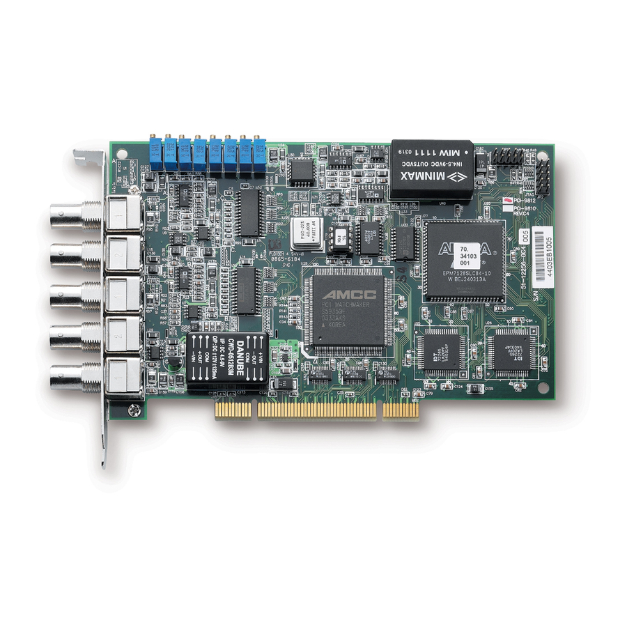
Page 19: Pci-9812/10'S Layout
2.3 PCI-9812/10's Layout Figure 2-1: PCB Layout of the PCI-9812/10 Installation... -
Page 20: Hardware Installation Outline
2.4 Hardware Installation Outline PCI configuration The PCI cards (or CompactPCI cards) are equipped with a Plug and Play PCI controller, it can request base addresses and interrupt according to PCI standard. The system BIOS will install the system resource based on the PCI cards’ configuration registers and system parameters (which are set by system BIOS). -
Page 21: Device Installation For Windows Systems
2.5 Device Installation for Windows Systems Once Windows 95/98/2000 has started, the Plug and Play function of Windows system will find the new NuDAQ/NuIPC cards. If this is the first time installing NuDAQ/NuIPC cards in your Windows system, you will be informed to enter the device information source. -
Page 23: Signal Connection
Signal Connection This chapter describes the connector of PCI-9812/10, the signal connection between PCI-9812/10 and external devices, and the switch setting for different applications. 3.1 Connectors PCI-9812/10 connects to external devices through five BNC connectors and one 10-pin dual-in-line header. Figure 3-1 shows the location of these connectors. -
Page 24: Table 3-1: Pin-Out Of Jp1
J4: The J4 BNC connector is used for the input signal of channel 3 A/D converter. J5: The J5 BNC connector is used for the input signal of external clock 0. JP1: The 10-pin connector is used for digital input signal, including one digital clock, one digital trigger and three digital inputs. -
Page 25: Analog Input Impedance Setting
3.2 Analog Input Impedance Setting This section describes the characteristics of the different inputs of the PCI-9812/10. Analog Input PCI-9812/10 has four analog input channels which are connected through connectors J1 - J4. The input impedance and input amplitude range can be changed through soldering the gap switches on board (refer to PCI-9812/10’s layout). - Page 26 CAUTION: 1. When the input channel is configured as a high impedance input, DO NOT leave the input connector unconnected. input connector must connected to a low impedance signal source to provide a return path for the input bias current, as the maximum input bias current of the OPAMP in the input stage is 35uA.
-
Page 27: External Clock 0
The corresponding switches and resistors of other channels are shown below: Channel Switches Resistor Channel 0 C0LO C05V Channel 1 C1LO C15V Channel 2 C2LO C25V Channel 3 C3LO C35V Table 3-4: Switches and Resistors External Clock 0 The external clock 0 (J5) is a sine wave signal, which is converted to a TTL signal inside the PCI-9812/10. -
Page 28: Digital Input
Digital Input PCI-9812/10 has four digital inputs: one external digital trigger (JP1 pin3) and three general-purpose digital inputs (JP1 pin5, 7, and 9). These inputs are TTL compatible with 10K-ohm pull-down resistors. Signal Connection... -
Page 29: Registers
Registers Descriptions of the register format and structure of the PCI-9812/ 10 are specified in this chapter. This information is useful for programmers who want to handle the card using low-level programming. 4.1 I/O Port Address PCI-9812/10 functions as a 32-bit PCI target device to any master on the PCI bus. -
Page 30: Adc Channel Enable Register
4.2 ADC Channel Enable Register PCI-9812/10 has four analog input channels - CH0, CH1, CH2, and CH3. CH0 - CH3 can be enabled or disabled by bit 0 - 3 of the ADC channel enable register. Address: BASE + 0 Attribute: write only Data Format: BASE+0... -
Page 31: Adc Clock Divisor Register
4.3 ADC Clock Divisor Register Feeding the ADC source clock to a clock frequency divider generates the ADC sampling clock. The output of the frequency divider becomes the sampling clock. The frequency of the ADC sampling clock is: Frequency of source clock / ADC clock divisor Address: BASE + 04h Attribute: write only Data Format:... -
Page 32: Trigger Mode Register
4.4 Trigger Mode Register The PCI-9812/10 has five trigger modes: software trigger, post trigger, pre-trigger, middle trigger and delay trigger. The trigger mode register is used to specify which trigger mode is currently used. Address: BASE + 08h Attribute: write only Data Format: Base + 8 TRGMOD2 TRGMOD1 TRGMOD0... -
Page 33: Trigger Level Register
4.5 Trigger Level Register The trigger condition of PCI-9812/10 includes trigger level and trigger slope. This register sets the trigger level, and the trigger source register described in the next paragraph sets the trigger slope. Address: BASE + 0ch Attribute: write only Data Format: BASE+Ch TRGLVL7 TRGLVL6 TRGLVL5 TRGLVL4 TRGLVL3 TRGLVL2 TRGLVL1 TRGLVL0... -
Page 34: Trigger Source Register
4.6 Trigger Source Register PCI-9812/10 supports five trigger sources - CH0, CH1, CH2, CH3, and external digital trigger. Address: BASE + 10h Attribute: write only Data Format: Base + 10 TRGSLP TRGSRC2 TRGSRC1 TRGSRC0 Base + 11 Base + 12 Base + 13 TRGSLP: trigger slope. -
Page 35: Post Trigger Counter Register
4.7 Post Trigger Counter Register The post trigger counter is a 16-bit down counter. The counter is pre-loaded with the value in the post trigger counter register and will count down on the rising edge of ADC sampling clock after the trigger condition is met. -
Page 36: Fifo Status Register
4.8 FIFO Status Register This register is used to monitor some status of the PCI-9812/10. Address: BASE + 18h Attribute: read Data Format: BASE+18h PTCO FIFOOR FIFOHF FIFOIR BASE+19h BASE+1Ah BASE+1Bh Bit 0 -- FIFOIR, FIFO input ready flag. 0: The FIFO is not ready for input, indicating FIFO is full 1: The FIFO is ready for input (not full). -
Page 37: Fifo Control Register
Bit 5 -- ACQ, acquisition flag 0: PCI-9812/10 is not acquiring data. Maybe the card is disabled or the card is waiting for trigger. 1: The PCI-9812/10 is acquiring data. Bit 6..31 -- Any value 4.9 FIFO Control Register This register is used to control the onboard FIFO memory. Address: BASE + 18h Attribute: write Data Format:... -
Page 38: Acquisition Enable Register
4.10 Acquisition Enable Register The register enables or disables the ADC acquisition. Address: BASE + 1ch Attribute: write only Data Format: BASE+18h ACQEN BASE+19h BASE+1Ah BASE+1Bh Bit 31..1 -- don't care Bit 0 -- ACQEN, acquisition enable When a "1" is written to this bit, the PCI-9812/10 is ready to sample data. -
Page 39: High Level Programming
Freq_Sel: 1: Frequency of A/D clock source is higher than PCI clock frequency (33 MHz) 0: Frequency of A/D clock source is lower than PCI clock frequency (33 MHz) CLKSRC2 CLKSRC1 Selected clock source Internal clock (40 MHz) External sine wave clock External digital clock Illegal Note:... -
Page 41: Operation Theory
Operation Theory The operation theorem of the functions on the PCI-9812/10 card is described in this chapter. The functions include A/D conversion and digital input. The operation theorem would assist the user understand, operate, and program the PCI-9812/10. 5.1 A/D Conversion Procedure Before programming the PCI-9812/10 to perform the A/D conversions, the user must first understand the following concepts:... -
Page 42: A/D Signal Source Control
data should be transferred into PC’s memory for further processing. PCI-9812/10 uses DMA to transfer the A/D data to host memory. Please refer to section 5.5. To process A/D data, programmers should be familiar with the A/D data format. Please refer to section 5.6. 5.2 A/D Signal Source Control To control the A/D signal source, the following three concepts should be understood: signal type, signal channel, and signal... -
Page 43: Trigger Sources
for the relationship between the 8-bit trigger level and the trigger voltage. The trigger is detected while the trigger event occurs. For Post- trigger and Middle-trigger, the data acquisition is performed after the trigger event; however, the time when the AD conversion starts is 350ns slower than the time when the trigger is detected. -
Page 44: Simultaneous Trigger For Multiple Cards
Positive-slope trigger event occurs External Digital Trigger An external digital trigger occurs when a rising edge or a falling edge is detected on the digital signal connected to pin3 of JP1 for external digital trigger. Simultaneous Trigger for Multiple Cards When multiple PCI-9812 cards are used in one system, the trigger sources of every card can be connected together to provide the function of simultaneous trigger for multiple cards. -
Page 45: Trigger Modes
Trigger Modes Software-Trigger Acquisition This trigger mode does not require any external trigger source. The trigger event occurs when the _9812_AD_DMA_Start( ) function is called to start the operation. Post-Trigger Acquisition Use post-trigger acquisition in applications where data needs to be collected after a specified trigger event. The trigger can either be an external analog trigger or digital trigger. -
Page 46: Figure 5-2: Pre-Trigger Acquisition
Figure 5-2: Pre-Trigger Acquisition Middle-Trigger Acquisition Use middle-trigger acquisition to collect data before and after a specified trigger event. The amount of data acquired before a trigger event occurs when using Middle trigger may not equal to the specified count of data, just like the pre-trigger mode. Figure 5-3: Middle-Trigger Acquisition The desired number of samples after trigger event is pre- loaded in post trigger counter register and will count down on... -
Page 47: A/D Clock Source Control
edge of ADC sampling clock after the trigger condition was met. When the count reaches 0, the counter stops and PCI-9812/10 starts to acquire data. Figure 5-4: Delay Trigger Acquisition 5.4 A/D Clock Source Control The AD clock source determines how the board regulates the timing of conversions when acquiring multiple samples from a single channel or from a group of multiple channels. -
Page 48: External Pacer Clock
clock. Feeding the clock source into a frequency divider generates the ADC sampling frequency. The following formula determines the ADC sampling frequency: Sampling Rate = Frequency of Source Clock / ADC Clock Divisor Note that the ADC Clock Divisor = 2,4,6,8,10… 65534 (maximum) External Pacer Clock Users can connect an external pacer clock to the EXTCLK1 (pin 1) on JP1 (for square wave) or Ext. -
Page 49: Ad Data Transfer
by 2) is used. Therefore, when the same external clock source is applied to multiple cards, the time difference of the sampling clocks between two cards will be half of the sampling clock period. The A/D clock cannot synchronize the multiple cards. 5.5 A/D Data Transfer AD Data Transfer For acquiring AD data, there are several function blocks on the... -
Page 50: Total Data Throughput
For one channel applications, only channel 0 can be selected with the total FIFO length being 32K samples. For simultaneous two- channel applications, use channel 0 and channel 1 to optimize the FIFO usage. The onboard circuit does not allow the user to use channel 0 and 2 or channel 2 and 3 simultaneously. -
Page 51: Bus-Mastering Data Transfer
the maximum data length would be either 16K or 8K samples, which is the maximum length from the size of onboard FIFO. Bus-mastering Data Transfer PCI bus-mastering DMA is necessary for high speed DAQ in order to utilize the maximum PCI bandwidth. The bus-mastering controller, which is built-in into the AMCC-5933 PCI controller ASIC, controls the PCI bus when it becomes the master of the bus. -
Page 52: Summary
Storing the data from host memory and into a hard disk or other storage devices should also be considered. The burst data rate of current HDD technology could be between 90 and 80MB/s. However in reality, the HDD effective bandwidth is usually less than 10MB/s, especially when the HDD seek time is longer, for example, 20ms, the FIFO is already full and the acquired data could not be continuous. -
Page 53: Ad Data Format
5.6 AD Data Format The A/D data of 12-bit PCI-9812 is on the 12 MSB of the 16-bit A/ D data. The 4 LSB of the 16-bit A/D data must be truncated by software (please refer to section 6.2). The relationship between the real signal voltage and the sampled value is shown in the following table: A/D Data... - Page 54 The formula between the A/D data and the analog value is Voltage = AD_data x (1/K) x (Gain) Where Gain and K are constants. For analog input range -1V to 1V, Gain =1 For analog input range -5V to 5V, Gain =5. For PCI-9812, K=2047x16=32752;...
-
Page 55: C++ Library
C/C++ Library This chapter describes the software library for operating this card. Only the functions in DOS library and Windows 95 DLL are described. Please refer to the PCIS-DASK function reference manual in the ADLINK CD for descriptions of the Windows 98/NT/ 2000 DLL functions. -
Page 56: Data Types
To differentiate between DOS libraries and Windows 95 libraries, a capital "W" is placed in the beginning of each function name of the Windows 95 DLL driver. e.g. W_9812_Initial(). Data Types Some data types were defined in Pci_9812.h (DOS) and Acl_pci.h (Windows 95). -
Page 57: 9812_Initial
6.3 _9812_Initial @ Description This function is used to initialize PCI-9812/10. Every PCI-9812/ 10 has to be initialized by this function before calling other functions. @ Syntax C/C++ (DOS) int _9812_Initial (int card_number, U16 *op_base_address,U16 *pt_base_address, U16 *irq_no, U16 *pci_master) C/C++ (Windows 95) int W_9812_Initial (int card_number, U16 *op_base_address,U16 *pt_base_address, U16... -
Page 58: 9812_Close
pci_master: BIOS enables or disables bus mastering in PCI Command Register @ Return Code PCICardNumErr PCIBiosNotExist PCIBaseAddrErr NoError 6.4 _9812_Close @ Description This function is used to close a previously initialized 9812 card. @ Syntax C/C++ (DOS) int _9812_Close (int card_number) C/C++ (Windows 95) int W_9812_Close (int card_number) Visual Basic (Windows 95) -
Page 59: 9812_Ad_Dma_Start
6.5 _9812_AD_DMA_Start @ Description This function will start an operation of A/D conversion N times with DMA data transfer. It will take place in the background, which will not stop until the Nth conversion has been completed or until your program executes _9182_AD_DMA_Stop to stop the operation. - Page 60 buff (DOS): The start address of the memory buffer to store the A/D data. The buffer size must be larger than the number of A/D conversions. This memory should be in double word alignment. The resolution of A/D data is 12-bit for 9812 and 10-bit for 9810.
-
Page 61: 9812_Ad_Dma_Status
count: The number of A/D conversion. @ Return Code PCICardNumErr,PCICardNotInit InvalidDMACnt,BufNotDWordAlign DMATransferNotAllowed,NoError 6.6 _9812_AD_DMA_Status @ Description Since _9812_AD_DMA_Start is executed in the background, the function _9812_AD_DMA_Status can be used to check its operation status. @ Syntax C/C++ (DOS) int _9812_AD_DMA_Status(int card_number, int *count, int *status, U32 *start_idx) C/C++ (Windows 95) int W_9812_AD_DMA_Status(int card_number, int *count, int... - Page 62 1: DMA_continue 2: DMA_wait_trig 3: DMA_wait_delay start_idx: The index where the data starts from is in the user’s buffer, i.e the sequence of read data is: buff[start_idx], buff[start_idx+1], _, buff[0], buff[1],_.,buff[start_idx-1]. @ Return Code PCICardNumErr PCICardNotInit NoError C/C++ Library...
-
Page 63: 9812_Ad_Dma_Stop
6.7 _9812_AD_DMA_Stop @ Description This function is used to stop the DMA data transfer. After executing this function, the _9812_AD_DMA_Start function stops. The function returns the number of data that has been transferred, whether the A/D DMA data transfer is stopped by this function or by the DMA terminal count ISR. -
Page 64: 9812_Set_Clk_Src
6.8 _9812_Set_Clk_Src @ Description This function is used to specify the ADC clock source. @ Syntax C/C++ (DOS) int _9812_Set_Clk_Src (int card_number, int clk_src, int ftpci) C/C++ (Windows 95) int W_9812_Set_Clk_Src (int card_number, int clk_src, int ftpci) Visual Basic (Windows 95) W_9812_Set_Clk_Src (ByVal card_number As Long, ByVal clk_src As Long, ByVal ftpci As Long) As Long @ Argument... -
Page 65: 9812_Set_Clk_Rate
@ Return Code PCICardNumErr PCICardNotInit InvalidClkSrc,NoError 6.9 _9812_Set_Clk_Rate @ Description This function is used to specify the clock divider for ADC clock. The valid number of the clock divider should be in the range of 2, 4, 6, 8, …., 65534. @ Syntax C/C++ (DOS) int _9812_Set_Clk_Rate (int card_number, U16 clk_div) -
Page 66: 9812_Set_Trig
6.10 _9812_Set_Trig @ Description This function is used to set up a trigger. The function specifies the trigger mode, trigger level (voltage), trigger source, trigger slope, and post trigger count. Please refer to sections 4.4 to 4.7 for further details on trigger setting. @ Syntax C/C++ (DOS) int _9812_Set_Trig (int card_number, int trig_mode, int trig_src,... - Page 67 trig_src: Selected trigger source, the valid trigger sources are: CH0_TRIG: Channel 0 CH1_TRIG: Channel 1 CH2_TRIG: Channel 2 CH3_TRIG: Channel 3 AUX_TRIG: External digital trigger trig_pol: Trigger slope. 0: Positive slope trigger 1: Negative slope trigger trig_lvl: Trigger level. The relationship between the 8-bit trigger level and the trigger voltage is shown in section 4.5.
-
Page 68: W_9812_Alloc_Dma_Mem
6.11 W_9812_Alloc_DMA_Mem @ Description Contacts the Windows 95 system to allocate a block of contiguous memory for DMA transfer. This function is only available in Windows 95. @ Syntax C/C++ (Windows 95) W_9812_Alloc_DMA_Mem (U32 buf_size, HANDLE *memID, U32 *linearAddr) Visual Basic (Windows 95) W_9812_Alloc_DMA_Mem (ByVal buf_size As Long, memID As Long, linearAddr As Long) As Long @ Argument... -
Page 69: W_9812_Free_Dma_Mem
6.12 W_9812_Free_DMA_Mem @ Description Releases a system DMA memory under Windows 95 environment. This function is only available in Windows 95. @ Syntax C/C++ (Windows 95) int W_9812_Free_DMA_Mem (HANDLE memID) Visual Basic (Windows 95) W_9812_Free_DMA_Mem (ByVal memID As Long) As Long @ Argument memID: The memory ID of the system DMA... -
Page 70: W_9812_Get_Sample
6.13 W_9812_Get_Sample @ Description For languages without pointer support such as Visual Basic, programmers can use this function to access the data in DMA buffer. This function is only available in Windows 95. @ Syntax C/C++ (Windows 95) int W_9812_Get_Sample (U32 linearAddr, U32 index, I16 *ai_data) Visual Basic (Windows 95) W_9812_Get_Sample (ByVal linearAddr As Long, ByVal idx As... -
Page 71: Calibration
Calibration In data acquisition, calibrating your measurement devices to maintain the accuracy is very important. Users can calibrate the analog input and analog output channels under the users' operating environment to optimize the accuracy. This chapter describes the calibration process for PCI-9812/10. 7.1 What you need The following equipment would be required for the process: Calibration utility: The program would guide the user... -
Page 72: A/D Calibration
7.3 A/D Calibration AD Calibration for Channel 0 1. Apply a +1V input signal to A/D channel 0, and trim the VR5 until the average reading of channel 0 is within the ± ± range of 2046.6 0.1 (9812) or 510.9 0.1 (9810). -
Page 73: Software Utility
Software Utility A utility program 9812util.exe is included in the software CD. This program has three functions, System Configuration, Calibration, and Functional Testing. This utility is designed as menu-driven based windowing style, that is, it provides not only the text messages for operating guidance, but also graphics to instruct the user on setting the hardware configuration correctly. -
Page 74: System Configuration
8.2 System Configuration Use the functions in System Configuration to configure your PCI- 9812/10 card. The following diagram will be displayed on the screen when the Configuration function is chosen from main menu. 8.3 Calibration This function takes the user through the calibration process of PCI-9812/10. - Page 75 selecting one of the calibration items from the menu, a calibration window will appear. The upper window shows the step-by-step calibration instructions. The lower window shows the layout of PCI-9812/10. In addition, the proper Variable Resister (VR) will blink to indicate the related VR needs to be adjusted for the current calibration step.
-
Page 76: Functional Testing
8.4 Functional Testing This function is used to test the functions of PCI-9812/10 A/D. When choosing a testing function from the main menu list, a function testing test window is displayed on the screen. The following is an example of a testing window. Software Utility... - Page 77 The setting of trigger mode, trigger signal polarity, trigger level, channel number and post trigger count (for middle trigger and delay trigger) can be adjusted or changed by using the keys indicated. After finishing adjusting these settings, press “Enter” to start performing the test function.
- Page 78 Software Utility...
-
Page 79: Warranty Policy
Warranty Policy Thank you for choosing ADLINK. To understand your rights and enjoy all the after-sales services we offer, please read the following carefully. 1. Before using ADLINK’s products please read the user manual and follow the instructions exactly. When sending in damaged products for repair, please attach an RMA application form which can be downloaded from: http:// rma.adlinktech.com/policy/. - Page 80 3. Our repair service is not covered by ADLINK's two-year guarantee in the following situations: Damage caused by not following instructions in the user's manual. Damage caused by carelessness on the user's part during product transportation. Damage caused by fire, earthquakes, floods, lightening, pollution, other acts of God, and/or incorrect usage of voltage transformers.
Need help?
Do you have a question about the NuDAQ PCI-9810 and is the answer not in the manual?
Questions and answers