Sign In
Upload
Manuals
Brands
ADLINK Technology Manuals
PCI Card
NuDAQ PCI-9812
ADLINK Technology NuDAQ PCI-9812 Manuals
Manuals and User Guides for ADLINK Technology NuDAQ PCI-9812. We have
1
ADLINK Technology NuDAQ PCI-9812 manual available for free PDF download: User Manual
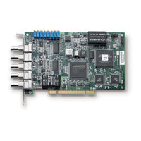
ADLINK Technology NuDAQ PCI-9812 User Manual (80 pages)
20MHz Simultaneous 4-CH Analog Input Card
Brand:
ADLINK Technology
| Category:
PCI Card
| Size: 0 MB
Table of Contents
Table of Contents
5
List of Tables
8
1 Introduction
11
Features
11
Applications
11
Specifications
12
Analog Input (A/D)
12
Digital Input
13
General Specifications
13
Software Support
14
Programming Library
14
PCIS-LVIEW: Labview® Driver
15
PCIS-VEE: HP-VEE Driver
15
Daqbenchtm: Activex Controls
15
Dasylabtm PRO
16
2 Installation
17
Checklist
17
Unpacking
18
PCI-9812/10'S Layout
19
Figure 2-1: PCB Layout of the PCI-9812/10
19
Hardware Installation Outline
20
PCI Configuration
20
PCI Slot Selection
20
Installation Instructions
20
Device Installation for Windows Systems
21
3 Signal Connection
23
Connectors
23
Figure 3-1: Location of Connectors
23
Table 3-1: Pin-Out of JP1
24
Table 3-2: Pin-Out of JP1 Connected to 9-Pin D-Type Connector
24
Analog Input Impedance Setting
25
Analog Input
25
Table 3-3: Analog Input
25
External Clock 0
27
External Clock 1
27
Table 3-4: Switches and Resistors
27
Digital Input
28
4 Registers
29
I/O Port Address
29
Table 4-1: I/O Address
29
ADC Channel Enable Register
30
ADC Clock Divisor Register
31
Trigger Mode Register
32
Table 4-2: Five Trigger Modes
32
Trigger Level Register
33
Table 4-3: Relationship between 8-Bit Trigger Level and Trigger Voltage
33
Trigger Source Register
34
Post Trigger Counter Register
35
FIFO Status Register
36
FIFO Control Register
37
Acquisition Enable Register
38
Clock Source Register
38
High Level Programming
39
Low Level Programming
39
5 Operation Theory
41
A/D Conversion Procedure
41
A/D Signal Source Control
42
A/D Trigger Source Control
42
Trigger Sources
43
Simultaneous Trigger for Multiple Cards
44
Trigger Modes
45
Figure 5-1: Post-Trigger Acquisition
45
Figure 5-2: Pre-Trigger Acquisition
46
Figure 5-3: Middle-Trigger Acquisition
46
A/D Clock Source Control
47
A/D Clock Sources
47
Internal Pacer Clock
47
Figure 5-4: Delay Trigger Acquisition
47
External Pacer Clock
48
Multiple Cards Operation
48
AD Data Transfer
49
Simultaneous Sampling of Four AD Channels
49
Figure 5-5: Block Diagram of PCI-9812
49
Total Data Throughput
50
Maximum Acquiring Data Length
50
Bus-Mastering Data Transfer
51
Host Memory Operation
51
Summary
52
AD Data Format
53
6 C++ Library
55
Libraries Installation
55
Programming Guide
55
Naming Convention
55
Nudaq PCI
55
Data Types
56
Table 6-1: Data Types
56
9812_Initial
57
9812_Close
58
9812_Ad_Dma_Start
59
9812_Ad_Dma_Status
61
9812_Ad_Dma_Stop
63
9812_Set_Clk_Src
64
9812_Set_Clk_Rate
65
9812_Set_Trig
66
W_9812_Alloc_Dma_Mem
68
W_9812_Free_Dma_Mem
69
W_9812_Get_Sample
70
7 Calibration
71
What You Need
71
VR Assignment
71
Table 7-1: Functions of Vrs
71
A/D Calibration
72
AD Calibration for Channel 0
72
AD Calibration for Channels 1,2,3
72
Table 7-2: AD Calibration for Channels 1,2,3
72
8 Software Utility
73
Running 9812Util.exe
73
System Configuration
74
Calibration
74
Functional Testing
76
Warranty Policy
79
Advertisement
Advertisement
Related Products
ADLINK Technology NuDAQ PCI-9111DG
ADLINK Technology NuDAQ PCI-9111HR
ADLINK Technology NuDAQ PCI-9114DG
ADLINK Technology NuDAQ PCI-9114HG
ADLINK Technology PCI-9524
ADLINK Technology NuDAQ PCI-9812/10
ADLINK Technology NuDAQ PCI-9810
ADLINK Technology NuDAQ PCI-9112
ADLINK Technology PCI-8366+
ADLINK Technology NuDAQ PCI-6308V
ADLINK Technology Categories
Computer Hardware
Motherboard
PCI Card
Control Unit
Desktop
More ADLINK Technology Manuals
Login
Sign In
OR
Sign in with Facebook
Sign in with Google
Upload manual
Upload from disk
Upload from URL