
Related Manuals for ADLINK Technology PCI-7230


Summary of Contents for ADLINK Technology PCI-7230
- Page 1 PCI-/cPCI-/LPCI-/LPCIe- 723X Series 32-CH Isolated Digital I/O Card User’s Manual Manual Rev. 4.05 Revision Date: June 24, 2008 Part No: 50-11037-1000 Advance Technologies; Automate the World.
- Page 2 Copyright 2008 ADLINK TECHNOLOGY INC. All Rights Reserved. The information in this document is subject to change without prior notice in order to improve reliability, design, and function and does not represent a commitment on the part of the manufacturer.
- Page 3 Getting Service from ADLINK Customer Satisfaction is top priority for ADLINK Technology Inc. Please contact us should you require any service or assistance. ADLINK TECHNOLOGY INC. Web Site: http://www.adlinktech.com Sales & Service: Service@adlinktech.com TEL: +886-2-82265877 FAX: +886-2-82265717 Address: 9F, No. 166, Jian Yi Road, Chungho City,...
-
Page 5: Table Of Contents
Table of Contents..............i List of Tables................iii List of Figures ................ iv 1 Introduction ................ 1 Features................2 PCI-7230, cPCI-7230, LPCI-7230, and LPCIe-7230 Fea- tures ..............2 PCI-7233 Features ............2 PCI-7234/7234P Features ..........3 PCI-7230/cPCI-7230/LPCI-7230/LPCIe-7230 Specifications ............4 Isolated Digital I/O (DIO) .......... - Page 6 PCI-7230 Pin Assignment ..........24 cPCI-7230 Pin Assignment ........... 26 LPCI/LPCIe-7230 Pin Assignment ........ 28 PCI-7233 Pin Assignment ..........30 PCI-7234 Pin Assignment ..........32 PCI-7234P Pin Assignment .......... 34 Termination Board Connection .......... 36 3 Register Format ..............37 PCI PnP Registers .............
-
Page 7: List Of Tables
List of Tables Table 3-1: I/O Address Map of PCI-7230/cPCI-7230/LPCI-7230/LP- CIe-7230 ..............38 Table 3-2: I/O Address Map of PCI-7233 ........ 38 Table 3-3: I/O Address Map of PCI-7234/7234P ..... 38 Table 3-4: Digital Input Register ..........39 Table 3-5: Digital Output Register ........... 40 Table 4-1: Differential Input circuits of cPCI-7230/LPCI-7230/LPCIe- 7230 ................ - Page 8 List of Figures Figure 2-1: PCI-7230 Pin Assignment........24 Figure 2-2: PCI-7230 Onboard Power and Ground terminal..25 Figure 2-3: cPCI-7230 Pin Assignment........26 Figure 2-4: LPCI/LPCIe-7230 Pin Assignment......28 Figure 2-5: PCI-7233 Pin Assignment........30 Figure 2-6: PCI-7233 Onboard Power and Ground terminal..31 Figure 2-7: PCI-7234 Pin Assignment........
-
Page 9: Introduction
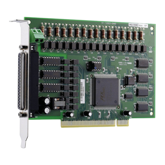
The PCI-7230/cPCI-7230/LPCI-7230/LPCIe-7230 provides 16 iso- lated inputs and 16 isolated outputs. The PCI-7230/cPCI-7230 iso- lated I/O channels are isolated to 5000 Vrms, and LPCI/LPCIe- 7230 isolated I/O channels are isolated to 2500 Vrms (excluding cables). -
Page 10: Features
PCI Express Interface (LPCIe-7230) 16 isolated Digital Input Channels 16 isolated Digital Output Channels High output driving capability 5000 Vrms high voltage isolation (for PCI-7230 and cPCI- 7230), 2500 Vrms high voltage isolation (for LPCI-7230 and LPCIe-7230) Two external interrupt sources... -
Page 11: Pci-7234/7234P Features
PCI-7234/7234P Features 32 Isolated Digital Output Channels High output driving capability 500 mA max@ 100% duty, for one of the eight transistor devices ON (PCI-7234: sink current, PCI-7234P: source current) 5,000 Vrms high voltage isolation 37-pin D-type connector Introduction... -
Page 12: Pci-7230/Cpci-7230/Lpci-7230/Lpcie-7230
Logic “L”: 0 to 1.5 V Logic “H”: 5 to 24 V Ω Input resistance:1.2 K @ 0.5 W Isolated voltage: 5000 Vrms (for PCI-7230 and cPCI-7230), 2500 Vrms (for LPCI-7230 and LPCIe-7230) Throughput:10 KHz Optical Isolated Output channel: Numbers of Channel: 16 digital outputs... -
Page 13: General Specifications
° Storage Temperature: -20 to 80 Humidity: 5 to 95%, non-condensing Power Consumption: PCI-7230: +5V @ 150 mA (typical) (Note: Requires external power) cPCI-7230: +5V @ 270 mA (typical) LPCI-7230: +5 V @ 150 mA (typical) LPCIe-7230: +3.3 V @ 279 mA (typical) -
Page 14: Pci-7233 Specifications
1.3 PCI-7233 Specifications Isolated Digital Input Optical Isolated Input Numbers of Channel: 32 digital inputs Input Voltage: up to 24Vdc Logic “L”: 0 to 1.5V Logic “H”: 5 to 24V Ω Input resistance:1.2 K @ 0.5W Isolated voltage: 5000Vrms Throughput: 10KHz Dual-interrupt sources: Change-of-state (COS) on any 16 DI lines of LSB Change-of-state (COS) on any 16 DI lines of MSB... -
Page 15: Pci-7234/7234P Specifications
1.4 PCI-7234/7234P Specifications Isolated Digital Output Numbers of Channel: 32 digital output Output type: Darlington transistors Output Voltage: open collector 5 V (min.), up to 35 V (max.) Sink Current: (PCI-7234) 500 mA max @ 100% duty, for one of the eight transis- tors ON 500 mA @ duty 20% for all transistors devices ON (Note: the pulse width is 25ms for one duty cycle) -
Page 16: Software Support
1.5 Software Support ADLINK Technology Inc., a leading provider of high-performance, high-quality data acquisition cards and platforms, delivers robust software support for its comprehensive line of DAQ cards with varying form factors including PCI Express®, PCI, CompactPCI, and PXI. ADLINK offers support not only for mainstream Windows and Linux OS, but also for third-party applications including Lab- VIEW®... -
Page 17: Windows Drivers
Windows Drivers ADLINK Task-oriented DAQ Driver/SDK and Wizard for Win- dows DAQPilot provides one interface for all ADLINK DAQ products via DAQPilot API DAQPilot ActiveX Control DAQPilot .Net Assembly, DAQPilot (Download and install from the DAQPilot product page: http://www.adlinktech.com/TM/DAQPilot.html Save development time Shorten learning curve DAQPilot is a driver and SDK with a graphics-driven interface for various ADE. - Page 18 immediately program ADLINK DAQ modules and integrate tasks to their own DAQ applications. Note: ADLINK strongly recommend all users to install the new- generation ADLINK Driver – DAQPilot instead legacy DASK drivers. For those users who have been using the legacy ADLINK DASK Drivers or are not able to connect to the in- ternet, you still can get the latest update from ADLINK all-in- one CD.
- Page 19 Configuration-Based Device Manager for ADLINK DAQ Cards DAQMaster (.\Utility) The ADLINK DAQMaster is a smart device manager that enables access to ADLINK data acquisition and test and measurement products. DAQMaster delivers an all-in-one configurations, user can get a full support matrix to well configure ADLINK Test and Measurement products.
- Page 20 ADLINK Legacy DAQ Card Drivers and SDK for Windows PCIS-DASK (.\Software Package\PCIS-DASK) D2K-DASK (.\Software Package\D2K-DASK) WD-DASK (.\Software Package\WD-DASK) User Mode Kernel Mode Delphi Process Structure DASK Kernel Driver PCIS-DASK (.sys) Object Manager VC++ Memory Executive D2K-DASK Manager Support Configuration Power Plug and Pay Manager Manager...
- Page 21 DASK also supports the following: Supports Windows Vista 32- or 64-bit editions Supports AMD64 and Intel x86-64 architectures Digitally-signed for Windows Vista 64-bit Edition Utilizes WOW64 subsystem to ensure that 32-bit applica- tions run normally on 64-bit Editions of Windows XP, Win- dows 2003 Server, and Windows Vista without modification.
-
Page 22: Linux Drivers
Linux Drivers Linux Drivers for ADLINK DAQ Cards Drivers are available on the ADLINK website: PCIS-DASK/X D2K-DASK/X WD-DASK/X ADLINK's DASK/X drivers are intended for developing customized data acquisition applications under Linux environments. The DASK/X drivers provide common APIs for ADLINK's extensive family of PCI, CompactPCI, and PXI plug-in data acquisition cards, and utilize the full capabilities of these cards under Linux environment. -
Page 23: Third-Party Software Support
Third-party Software Support MATLAB® Data Acquisition Toolbox Adapter for ADLINK DAQ Cards DAQ-MTLB for MATLAB® (.\Software Package\DAQ- MTLB) DAQ-MTLB MATLAB® integrates ADLINK components with MATLAB® Data Acquisition Toolbox and enables users to control a wide range of ADLINK DAQ cards directly from the advanced MATLAB®... - Page 24 LabVIEW™ Data Acquisition VI Set for ADLINK DAQ Cards DAQ Cards DAQ-LVIEW PnP for LabVIEW™ (.\Software Package\DAQ-LVIEW PnP) The DAQ-LVIEW PnP is a set of LabView Virtual Instruments (Vis) that is fully-compatible with National Instrument's DAQ VIs. Based on the virtual instruments concept, DAQ-LVIEW PnP provides four additional tool panels in LabView, including analog input, analog output, digital I/O, and timer/counter.
-
Page 25: Vee™ Interface For Adlink Daq Cards
VEE™ Interface for ADLINK DAQ Cards PCIS-VEE (.\Software Package\PCIS-VEE) D2K-VEE (.\Software Package\D2K-VEE) Agilent VEE™ is a popular visual programming environment for data acquisition that includes data analysis and control. VEE pro- vides a visual programming interface that allows users to create programs by connecting objects such as acquisition routines, but- tons and displays in a flow diagram. -
Page 26: Componentware/Activex Control
Componentware/ActiveX Control 32-Bit ActiveX Controls for Measurement and SCADA/HMI DAQBench (.\Software Package\DAQBench) DAQBench is a specialized ActiveX control package designed for 32-bit measurement and SCADA/HMI applications. DAQBench leverages the power of the latest Microsoft ActiveX technology - the standard for code interchangeability and integration under var- ious Windows platform. -
Page 27: Applications For Test And Measurement
Applications for Test and Measurement Smart & Easy-to-Use Data Acquisition System Creator DAQCreator (.\Software Package\DAQCreator) DAQCreator is an out-of-the-box data acquisition software for acquiring, displaying, analyzing, and storing data from ADLINK DAQ cards. Equipped with a smart wizard and intuitive panels, users can easily configure data acquisition settings, change the appearance of data display, perform FFT to acquired data, and store data to a hard disk drive. - Page 28 Introduction...
-
Page 29: Installation
Installation This chapter describes the configurations of the PCI-/cPCI-/LPCI-/ LPCIe-723X Series. The PCI-/cPCI-/LPCI-/LPCIe-723X Series is Plug and Play and can easily be installed onto any PC system with PCI slots. 2.1 What You Have This User’s Manual PCI-/cPCI-/LPCI-/LPCIe-723X Series Isolated Digital I/O Card ADLINK CD Software Installation Guide... -
Page 30: Hardware Installation Outline
2.3 Hardware Installation Outline PCI configuration The PCI cards (or CompactPCI cards) are equipped with a Plug and Play PCI controller, it can request base addresses and inter- rupt in accordance with the PCI standard. The system BIOS will install the system resource based on the PCI cards’ configuration registers and system parameters (which are set by system BIOS). -
Page 31: Device Installation For Windows Systems
2.4 Device Installation for Windows Systems Once Windows Vista/XP/2003/2000 has started, the Plug and Play function of Windows system will find the new NuDAQ/NuIPC cards. If this is the first time installing NuDAQ/NuIPC cards on your Windows system, you will be prompted to enter the device information source. -
Page 32: Connector Pin Assignment
EOGND IDO_0 (11) (30) IDO_1 IDO_2 (12) (31) IDO_3 IDO_4 (13) (32) IDO_5 IDO_6 (14) (33) IDO_7 IDO_8 (15) (34) IDO_9 IDO_10 (16) (35) IDO_11 IDO_12 (17) (36) IDO_13 IDO_14 (18) (37) IDO_15 (19) Figure 2-1: PCI-7230 Pin Assignment Installation... -
Page 33: Figure 2-2: Pci-7230 Onboard Power And Ground Terminal
VDD: Power supply of isolated output channels. The VDD must be supplied by an external power sup- Note: ply of 5 to 35VDC. E O G N D E O G N D Figure 2-2: PCI-7230 Onboard Power and Ground terminal Installation... -
Page 34: Cpci-7230 Pin Assignment
cPCI-7230 Pin Assignment The pin assignment of the cPCI-7230’s 50 pins SCSI-II type con- nector CN1 is shown in the following diagram. (26) EOGND (27) EOGND EOGND EOGND (28) EOGND (29) EOGND IDO_7 (30) IDO_14 IDO_6 (31) IDO_15 IDO_5 (32) IDO_12 IDO_4 (33) - Page 35 EICOM: Common ground or common power of isolated input channels #8 to 15. IDI_nH: High input of isolated differential DI channel #n. IDI_nL: Low input of isolated differential DI channel #n. EOGND: Ground return path of isolated output channels. VDD: Power input signal for fly-wheel diode of DO channels. Installation...
-
Page 36: Lpci/Lpcie-7230 Pin Assignment
LPCI/LPCIe-7230 Pin Assignment The pin assignment of the LPCI-7230’s 50 pins SCSI-II type con- nector CN1 is shown in the following diagram. (26) (26) (26) (26) ISO5V ISO5V ISO5V EIGND EIGND EICOM EOGND (27) (27) (27) (27) ISO5V EIGND EIGND EOGND (28) (28) - Page 37 EICOM: Common ground or common power of isolated input channels #8 to 15. IDI_nH: High input of isolated differential DI channel #n. IDI_nL: Low input of isolated differential DI channel #n. EOGND: Ground return path of isolated output channels. VDD: Power input signal for fly-wheel diode of DO channels. ISO5V: Isolatied power output 5V.
-
Page 38: Pci-7233 Pin Assignment
PCI-7233 Pin Assignment The pin assignment of the 37 pins D-type connector CN1 is illus- trated below: IDI_0 (20) IDI_1 IDI_2 (21) IDI_3 IDI_4 (22) IDI_5 IDI_6 (23) IDI_7 IGND (24) IDI_8 IDI_9 (25) IDI_10 IDI_11 (26) IDI_12 IDI_13 (27) IDI_14 IDI_15 (28) -
Page 39: Figure 2-6: Pci-7233 Onboard Power And Ground Terminal
I.GND Figure 2-6: PCI-7233 Onboard Power and Ground terminal Installation... -
Page 40: Pci-7234 Pin Assignment
PCI-7234 Pin Assignment The pin assignment of the 37 pins D-type connector CN1, which is an isolated DIO signal connector, is shown below. IDO_0 (20) IDO_1 IDO_2 (21) IDO_3 IDO_4 (22) IDO_5 IDO_6 (23) IDO_7 I.GND (24) IDO_8 IDO_9 (25) IDO_10 IDO_11 (26) -
Page 41: Figure 2-8: Pci-7234 Onboard Power And Ground Terminal
I.GN I.GND Figure 2-8: PCI-7234 Onboard Power and Ground terminal Installation... -
Page 42: Pci-7234P Pin Assignment
PCI-7234P Pin Assignment The pin assignment of the 37 pins D-type connector CN1, which is an isolated DIO signal connector, as shown below: IDO_0 (20) IDO_1 IDO_2 (21) IDO_3 IDO-4 (22) IDO_5 IDO_6 (23) IDO_7 (24) IDO_8 IDO_9 (25) IDO_10 IDO_11 (26) IDO_12... -
Page 43: Figure 2-10: Pci-7234P Onboard Power And Ground Terminal
I.GND I.GND Figure 2-10: PCI-7234P Onboard Power and Ground terminal Installation... -
Page 44: Termination Board Connection
2.6 Termination Board Connection The 723X boards are equipped with a DB-37 or a 50-pin SCSI-II female connector. Available termination boards include: ACLD-9137-01: General-Purpose termination board with a 37-pin D-sub male con- nector. DIN-37D-01: Termination board with a 37-pin D-sub connector and DIN-Rail mounting (including one 1-meter ACL-10137 cable). -
Page 45: Register Format
Register Format The registers format is described in this chapter. This information is quite useful for programmers who wish to handle the card by low-level programming. However, it is recommended that the user has a deeper understanding of the PCI interface before starting any low-level programming. -
Page 46: I/O Registers Format
Address Write Read Base (0 - 1 ) Isolated DO Isolated DI Table 3-1: I/O Address Map of PCI-7230/cPCI-7230/LPCI-7230/LPCIe-7230 The PCI-7233 requires one 32-bit address in the PC I/O address space. Table 3.2 shows the address. Address Write Read Base (0 - 3 ) -
Page 47: Digital Input Register
3.3 Digital Input Register There is a total of 16 and 32 digital input channels on the PCI- 7230/cPCI-7230/LPCI-7230/LPCIe-7230 and PCI-7233 respec- tively. Each bit corresponds to a signal on the digital input channel. IDI_16 to IDI_31 are only available on PCI-7233. Address: BASE + 0 to BASE + 3 Attribute: read only Data Format:... -
Page 48: Digital Output Register
3.4 Digital Output Register There is a total of 16 and 32 digital output channels on the PCI- 7230/cPCI-7230/LPCI-7230/LPCIe-7230 PCI-7234/7234P respectively. Each bit corresponds to a signal on the digital output channel. IDO_16 to IDO_31 are only available on PCI-7234/ 7234P. -
Page 49: Operation Theory
The input can accept voltages of up to 24 V. The input resisters on PCI-7230/7233, cPCI-7230 and LPCI-7230/LPCIe-7230 are Ω 1.2 K . The connection between outside signal and PCI-7230/ 7233, cPCI-7230 and LPCI-7230/LPCIe-7230 are shown below. Isolated Input 1.2K Ohm... -
Page 50: Table 4-1: Differential Input Circuits Of Cpci-7230/Lpci-7230/Lpcie-7230
1.2K Ohm DI_nH DI_nL Table 4-1: Differential Input circuits of cPCI-7230/LPCI-7230/LPCIe-7230 Operation Theory... -
Page 51: Isolated Digital Output Circuits
4.2 Isolated Digital Output Circuits On the 7230/7234 series, an external voltage source, minimum 5V, maximum 35 VDC, is necessary to power the internal isolated circuits. It is connected with the VDD pin, When the isolated digital output goes to high, the sink current will be from VDD. On the 7230/7234 series, the VDD pin is used as a “fly-wheel”... -
Page 52: Figure 4-4: Isolation Output To Ttl Input Connection
Figure 4-4: Isolation Output to TTL Input connection Operation Theory... -
Page 53: Figure 4-5: Isolation Output To Isolation Input Connection
Figure 4-5: Isolation Output to Isolation Input connection Operation Theory... -
Page 54: Change Of State Detection
4.3 Change of State Detection What is COS? The COS (Change of State) occurs when the input state (logic level) is changed from low to high or from high to low. The COS detection circuit is used to detect the edge of level change. In the PCI-7233 card, the COS detection circuit is applied to all 32 chan- nels input channels. -
Page 55: Figure 4-6: Dual Interrupt System Of Pci-7233
DI_0~ INT1 DI_15 DI_0~ PLD1 DI_31 Channel Bridge Clear Isolated Input DI_16~ INT2 DI_31 PLD2 PCI Bus Figure 4-6: Dual Interrupt System of PCI-7233 Operation Theory... -
Page 56: Cos Detection
COS Detection The following timing is an example of the COS detection. Every DI signal’s edge change can be detected. All the DI channels edge will be ‘OR’ together to generate the INT1 or INT2 IRQ signals. If INT1 or INT2 irq Signals generate, the signal will be latch its state.
Need help?
Do you have a question about the PCI-7230 and is the answer not in the manual?
Questions and answers