
Related Manuals for ADLINK Technology NuDAQ PCI-7396


Summary of Contents for ADLINK Technology NuDAQ PCI-7396
- Page 1 NuDAQ P C I - 7 3 9 6 DIN-96DI, DIN-96DO 96-CH Digital I/O Cards U s e r ’ s G u i d e...
- Page 3 This document contains proprietary information protected by copyright. All rights are reserved. No part of this manual may be reproduced by any mechanical, electronic, or other means in any form without prior written permission of the manufacturer. Trademarks NuDAQ , DAQBench registered trademarks ADLINK Technology Inc.
- Page 4 Customer Satisfaction is always the most important thing for ADLINK Tech Inc. If you need any help or service, please contact us and get it. ADLINK Technology Inc. Web Site http://www.Adlink.com.tw Sales & Service service@Adlink.com.tw Technical NuDAQ nudaq@Adlink.com.tw Support NuDAM nudam@Adlink.com.tw NuIPC nuipc@Adlink.com.tw NuPRO nupro@Adlink.com.tw...
-
Page 5: Table Of Contents
CONTENTS How to Use This Guide ..........iv Chapter 1 Introduction ..........1 Features................1 1.1.1 Digital I/O Ports................1 1.1.2 Timer / Counter and Interrupt System........1 1.1.3 Miscellaneous..................2 Applications................ 2 Specifications..............2 Software Supporting............3 1.4.1 Programming Library..............3 ® 1.4.2 PCIS-LVIEW: LabVIEW Driver ...........3 1.4.3 PCIS-VEE: HP-VEE Driver............4... - Page 6 I/O Address Map..............14 Digital Data Registers ............15 Control Register............... 15 External Trigger Enable Register........17 External Trigger Disable Register........17 Change of State (COS) Control Register ......17 Interrupt Source Control (ISC) Register......18 Clear Interrupt Register ............ 18 3.10 Timer/Counter Register.............
- Page 7 5.10 _7396_CLR_IRQ..............34 5.11 _7396_Set_Event_Edge ............. 35 5.12 _7396_Cascaded_Timer ............ 35 5.13 _7396_Timer_Start ............36 5.14 _7396_Timer_Read............37 Appendix A1 DIN-96DI ..........38 A1.1 Introductions..............38 A1.2 Features................38 A1.3 Specifications..............38 A1.4 Layout of DIN-96DI ............39 A1.5 DI Circuits and Wiring............40 Appendix A2 DIN-96DO ...........41 A2.1 Introductions..............
-
Page 8: How To Use This Guide
How to Use This Guide This manual is designed to help you use the PCI-7396. It describes how to modify and control various functions on the PCI-7396 card to meet your requirements. It is divided into three chapters: Chapter 1, "Introduction," gives an overview of the product features. applications, and specifications. -
Page 9: Chapter 1 Introduction
Introduction The PCI-7396 is a 48/96-bit parallel digital input/output (DIO) card designed for industrial applications. The plug and play feature of PCI- Bus architecture make it easy for users to install their systems quickly. The PCI-7396 emulates two/four 8255 Programmable Peripheral Interface (PPI) chips. -
Page 10: Miscellaneous
48/96-bit change of state (COS) interrupt Dual interrupt system 1.1.3 Miscellaneous Provide 12V and 5V power supply on SCSI-type 100-pin connectors(only for PCI-7348) On board resettable fuses to protect power supply from external damage. (only for PCI-7348) Applications Programmable mixed digital input & output Industrial monitoring and controlling LED indicator driving Parallel data transfer... -
Page 11: Software Supporting
Software Supporting ADLink provides versatile software drivers and packages for users’ different approach to built-up a system. We not only provide programming library such as DLL for many Windows systems, but ® also provide drivers for many software package such as LabVIEW HP VEE , DASYLab , InTouch... -
Page 12: Pcis-Vee: Hp-Vee Driver
board. You can install and use them without license. For detail information about PCIS-LVIEW, please refer to the user’s guide in the CD. (\\Manual_PDF\Software\PCIS-LVIEW) 1.4.3 PCIS-VEE: HP-VEE Driver The PCIS-VEE includes the user objects, which are used to interface with HP VEE software package. PCIS-VEE supports Windows 95/98/NT. -
Page 13: Pcis-Opc: Opc Server
1.4.8 PCIS-OPC: OPC Server PCIS-OPC is an OPC Server, which can link with the OPC clients. There are many software packages on the market can provide the OPC clients now. The PCIS-OPC supports the Windows NT. It needs license. Introduction 5... -
Page 14: Chapter 2 Installation
Installation This chapter describes how to install the PCI-7396. The contents in the package and unpacking information that you should be careful are described. Please follow the steps to install the PCI-7348/7396. w Check what you have (section 2.1) w Unpacking (section 2.2) w Check the PCB (section 2.3) w Install the hardware (section 2.4) w Please refer to the “Software Installation Guide”... -
Page 15: Unpacking
Unpacking Your PCI-7396 card contains sensitive electronic components that can be easily damaged by static electricity. The card should be done on a grounded anti -static mat. The operator should be wearing an anti -static wristband, grounded at the same point as the anti-static mat. -
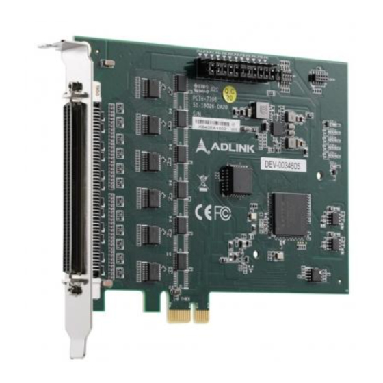
Page 16: Pci-7396 Layout
PCI-7396 Layout Figure 2.1 PCI-7396 Layout Installation... -
Page 17: Hardware Installation Outline
Device Installation for Windows Systems Once Windows 95/98/2000 has started, the Plug and Play function of Windows system will find the new NuDAQ/NuIPC cards. If this is the first time to install NuDAQ/NuIPC cards in your Windows system, you will be informed to input the device information source. Please refer to the “Software Installation Guide”... -
Page 18: Connectors' Pin Assignment
Connectors’ Pin Assignment (1) P1A0 (26) P2A0 (51) P3A0/EVENT (76) P4A0 (2) P1A1 (27) P2A1 (52) P3A1 (77) P4A1 (51) (52) (3) P1A2 (28) P2A2 (53) P3A2 (78) P4A2 (53) (4) P1A3 (29) P2A3 (54) P3A3 (79) P4A3 (5) P1A4 (30) P2A4 (55) P3A4 (80) P4A4 (6) P1A5 (31) P2A5 (56) P3A5 (81) P4A5... -
Page 19: Jumpers' Description
Jumpers’ Description The PCI-7396 is a ‘plug and play’ add-on card using PCI bus. It is un-necessary for user to setup its base address and IRQ level to fit the hardware of your computer system. However, to fit users’ versatile operation, there are still a few jumpers to set the power-on-states of all I/O ports. -
Page 20: Termination Boards Supporting
Termination Boards Supporting PCI-7396 can be connected with several different daughter boards, including DIN-100S, DIN-96DI, and DIN-96DO. The functionality and connections are specified as follows. 2.8.1 Connect with DIN-100S DIN-100S is a direct connector for the add-on card that is equipped with SCSI-100 connector. -
Page 21: Chapter 3 Registers Format
Registers Format The detailed descriptions of the registers format are specified in this chapter. This information is quite useful for the programmers who wish to handle the card by low-level programming. However, we suggest user have to understand more about the PCI interface then start any low-level programming. -
Page 22: I/O Address Map
offset 18h of PCR. Therefore, users can read the 18h of PCR to know the base address by using the BIOS function call. Please do not try to modify the base address and interrupt which assigned by the PCI PnP BIOS, it may cause resource confliction in your system. -
Page 23: Digital Data Registers
Table 3.1 Register Map The PCI-7396 has 2/4 PPIs on board. Each PPI contains 5 registers, including Digital Data Registe r, Control Register, External Trigger Enable Register, External Trigger Disable Register, and COS Interrupt Control Register. In the following sections, the 5 registers of PPI1 will be introduced respectively. - Page 24 BASE+ 07h P1n : n: port number Set to be ‘0’ for input port , ‘1’ for output port Registers Format...
-
Page 25: External Trigger Enable Register
External Trigger Enable Register Users can write anything to this register to enable the external trigger to latch the input data of port A,B and C simultaneously. Note that when this register is enabled, the settings of the previous control register are disabled. -
Page 26: Interrupt Source Control (Isc) Register
P1n : n: port number Set to be ‘0’ to disable COS , ‘1’ to enable COS Interrupt Source Control (ISC) Register The PCI-7396 has a dual interrupt system, two interrupt sources can be generated and be distinguished by software setting. This register is used to select the interrupt sources. -
Page 27: Timer/Counter Register
BASE+54h BASE+55h BASE+56h BASE+57h 3.10 Timer/Counter Register The 8254 chip occupies 4 I/O addresses in the PCI-7396. Please refer to NEC's or Intel's data sheet for the full description of the 8254 operation. Address : BASE + 40h ~ BASE + 4Ch Attribute : read / write Data Format : Base + 40h... -
Page 28: Chapter 4 Operation Theorem
Operation Theorem The operation theorem of the functions on PCI-7396 card is described in this chapter. The operation theorem can help you to understand how to manipulate or to program the PCI-7396. Digital I/O Ports 4.1.1 Introduction The PCI-7396 has 2/4 PPIs on board. Each 24-bit PPI is divided into three 8-bit I/O ports: A, B, and C. -
Page 29: 8254 Timer/Counter Operation
EXTTRG Latch Data (Latch input data to registers) Read Data (Read date from registers to Figure 4.2 Read Data use External Trigger 8254 Timer/Counter Operation 4.2.1 Introduction One 8254 programmable timer/counter chip is installed in the PCI- 7396. There are three counters in one 8254 chip and 6 possible operation modes for each counter. -
Page 30: Cascaded 32 Bits Timer
4.2.2 Cascaded 32 bits Timer The base frequency of input clock for the cascaded timer is 2MHz. The output is send to be the timer interrupt. To set the maximum and minimum frequency of the timer, please refer to the function _7348_Cascaded_Timer or _ 7396_Cascaded_Timer. -
Page 31: Interrupt Source Control (Isc)
The two IRQ requests are named as INT1 and INT2. INT1 comes from COS P1 & P2, P1C0, P1C3, or the event counter interrupt. INT2 comes from COS P3 & P4, P2C0, P2C3, or the timer interrupt. The sources of INT1 and INT2 is selectable by using the Interrupt Source Control (ISC) Register. -
Page 32: Change Of State (Cos) Interrupt
Mode 3 2 ~P2C0 falling edge of P2C0 Mode 4 3 Timer Output Timer count down to 0 Table 4.1 ISC register format Default settings When the IRQ sources is set as “P1C0 OR ~P1C3” or “P2C0 OR ~P2C3”, the IRQ trigger conditions are summarized in Table 4.2, P1C0 P1C3 IRQ Trigger Condition... -
Page 33: And 5V Power Supply
COS Detection The following timing is an example of COS operation. All the DI signals’ level change will be detected and then take an ‘OR’ operation to generate the INT1 or INT2 IRQ request. If INT1 or INT2 IRQ request generates, the signal will be latched. User should apply the function “_7396_CLR_IRQ”... -
Page 34: Chapter 5 C/C++ Libraries
C/C++ Libraries This chapter describes the software library for operating this card. Only the functions in DOS library and Windows 95 DLL are described. Please refer to the PCIS-DASK function reference manual, which included in ADLINK CD, for the descriptions of the Windows 98/NT/2000 DLL functions. -
Page 35: Programming Guide
Programming Guide 5.2.1 Naming Convention The functions of the NuDAQ PCI cards or NuIPC CompactPCI cards’ software driver are using full-names to represent the functions' real meaning. The naming convention rules are: In DOS Environment : _{hardware_model}_{action_name}. e.g. _7396_Initial() . -
Page 36: 7396_Initial
_7396_Initial @ Description This function is used to initialize the PCI-7396. Every PCI-7396 has to be initialized by this function before calling other functions. @ Syntax C/C++ (DOS) U16 _7396_Initial (U16 *existCards, PCI_INFO *pciInfo) C/C++ (Windows 95) U16 W_7396_Initial (U16 *existCards, PCI_INFO *pciInfo) Visual Basic (Windows 95) W_7396_Initial (existCards As Integer, pciInfo As... - Page 37 @ Syntax C/C++ (DOS) _7396_DI (U16 cardNo, U16 channelPort, U32 *diData) C/C++ (Windows 95) W_7396_DI (U16 cardNo, U16 channelPort, U32 *diData) Visual Basic (Windows 95) W_7396_DI (ByVal cardNo As Integer, ByVal channelPort As Integer, diData As Integer) As Integer @ Argument cardNo: The card number of PCI7396 card initialized.
-
Page 38: 7396_Config_Port
@ Return Code ERR_NoError _7396_DO @ Description This function is used to write data to digital output ports. There are 6 ports (P1A, P1B, P1C, P2A, P2B, P2C) could be configured as digital outputs on the PCI-7348. And there are totally 12 digital output ports (P1A, P1B, P1C, P2A, P2B, P2C, P3A, P3B, P3C, P4A, P4B, P4C) could be configured as digital outputs on the PCI-7396. - Page 39 _7396_Config_Port (U16 cardNo, int ctrlValue) C/C++ (Windows 95) W_7396_Config_Port (U16 cardNo, int ctrlValue) Visual Basic (Windows 95) W_7396_Config_Port (ByVal cardNo As Integer, ByVal channelPort As Integer, ByVal direction As Integer) As Integer @ Argument cardNo : The card number of PCI7396 card initialized. ctrlValue : P1ARD : CH1’s Port A input port...
- Page 40 P4CRD : CH4’s Port C input port P4RD : CH4’s Port A,B,C input port E_P4RD : CH4’s Port A,B,C input port use external clock to latch data P4AWR : CH4’s Port A output port P4BWR : CH4’s Port B output port P4CWR : CH4’s Port C output port P4WR...
-
Page 41: 7396_Software_Reset
_7396_Software_Reset @ Description This function is used to reset the I/O port configuration. After resetting PCI-7396, all ports will be set as input ones. Note that this function will not re-start the PCI bus and all the hardware settings will not be changed, neither. -
Page 42: 7396_Cosirq_Control
c1 : INT1# interrupt source c2 : INT2# interrupt source For the C1,C2 settings, please refer to Table3.3.1 @ Return Code ERR_NoError _7396_COSIRQ_Control @ Description This function is used to programe every channel port A,B,C‘s COS is enable or disable. @ Syntax C/C++ (DOS) void _7396_COSIRQ_Control (U16 cardNo, int ch_no,... -
Page 43: 7396_Set_Event_Edge
Visual Basic(Windows 95) W_7396_CLR_IRQ (ByVal cardNo As Integer) @ Argument cardNo : The card number of PCI7396 card initialized. @ Return Code None 5.11 _7396_Set_Event_Edge @ Description This function is used to set the edge trigger of event signal (Pin51) and external trigger signal (Pin99). -
Page 44: 7396_Timer_Start
@ Description The function is used to program the timer#1 & timer#2 of 8254, the 32bit timer, to generate the timer interrupt . @ Syntax C/C++ (DOS) _7396_Cascaded_Timer (U16 *existCards, U16 c1, U16 c2) C/C++ (Windows 95) W_7396_Cascaded_Timer (U16 *existCards, U16 c1, U16 c2) Visual Basic (Windows 95) W_7396_Initial (existCards As Integer, ByVal c1 As... -
Page 45: 7396_Timer_Read
@ Argument cardNo: The card number of PCI7396 card initialized. timer_mode: 8254 operating mode c0: frequency divider of timer #0 @ Return Code ERR_NoError ERR_PCIBiosNotExist 5.14 _7396_Timer_Read @ Description This function is used to read the counter value of the Counter#0. @ Syntax C/C++ (DOS) U16 _7396_Timer_Read (U16 cardNo, U16 *c0) -
Page 46: Appendix A1 Din-96Di
DIN-96DI A1.1 Introductions DIN-96DI digital input termination board features high-voltage opto-isolation on all inputs to prevent floating potential and ground loop problems from damaging your PC system. It is composed of one TB-96 base board, one TB-96DI daughter board, and one DIN socket for easy maintenance, wiring, and installation. -
Page 47: A1.4 Layout Of Din-96Di
Storage temp.: -20 ~ 80 C Humidity: 5~95%, non-condensing Power consumption: 490mA(max.) for 24V PS 250mA(max.) for 12V PS 102mA(max.) for 5V PS A1.4 Layout of DIN-96DI TB-96DI TB96 DIN-96DI... -
Page 48: A1.5 Di Circuits And Wiring
Legend: : SCSI II 100 pin connector to connect PCI-7396 and DIN-96DI X1~X4 : 50 pin Opto-22 connectors to connect TB96 and Tb96DI n(1~96) : Input signal n : External ground : External power (5~24V) A1.5 DI Circuits and Wiring The outputs of the opto-isolated digital input circuits are open collector transistors. -
Page 49: Appendix A2 Din-96Do
DIN-96DO A2.1 Introductions DIN-96DO digital output termination board features high-voltage opto-isolation on all outputs to prevent floating potential and ground loop problems from damaging your PC system. It is composed of one TB-96 base board, one TB-96DO daughter board, and one DIN socket for easy maintenance, wiring, and installation. -
Page 50: A2.4 Layout Of Din-96Do
Storage temp.: -20 ~ 80 C Humidity: 5~95%, non-condensing Power consumption: 4.294A(max.) for 24VPS 4.244A(max.) for 12VPS 4.215A(max.) for 12VPS 102mA(max.) from cable A2.4 Layout of DIN-96DO TB-96DO TB96 DIN-96DI DO... -
Page 51: A2.5 Circuits And Wiring
Legend: : SCSI II 100 pin connector to connect PCI-7396 and DIN-96DO X1~X4 : 50 pin Opto-22 connectors to connect TB96 and Tb96DO n(1~96) : Output signal n : External ground : External power (5~24V) A2.5 Circuits and Wiring The connection of isolated digital output is shown as the following diagram. - Page 52 Power Inductance Loading 5~24V Figure A2.2: opto-isolated output circuit for inductance loading DIN-96DI DO...
-
Page 53: Product Warranty/Service
Product Warranty/Service Seller warrants that equipment furnished will be free form defects in material and workmanship for a period of one year from the confirmed date of purchase of the original buyer and that upon written notice of any such defect, Seller will, at its option, repair or replace the defective item under the terms of this warranty, subject to the provisions and specific exclusions listed herein.
Need help?
Do you have a question about the NuDAQ PCI-7396 and is the answer not in the manual?
Questions and answers