
Related Manuals for ADLINK Technology NuDAQ PCI-9114DG


Summary of Contents for ADLINK Technology NuDAQ PCI-9114DG
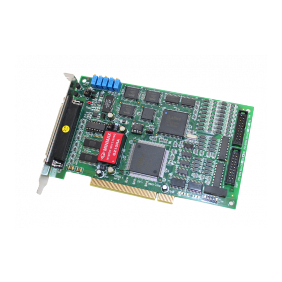
- Page 1 NuDAQ P C I - 9 1 1 4 D G / H G Enhanced Multi-Functions Data Acquisition Card User’s Guide...
- Page 3 Trademarks NuDAQ , NuIPC , DAQBench are registered trademarks of ADLink Technology Inc. Other product names mentioned herein are used for identification purposes only and may be trademarks and/or registered...
- Page 4 Customer Satisfaction is always the most important thing for ADLink Tech Inc. If you need any help or service, please contact us and get it. ADLink Technology Inc. Web Site http://www.adlink.com.tw Sales & Service service@adlink.com.tw Technical NuDAQ nudaq@adlink.com.tw Support NuDAM nudam@adlink.com.tw NuIPC nuipc@adlink.com.tw NuPRO nupro@adlink.com.tw...
-
Page 7: Table Of Contents
Table of Contents How to Use This Guide ..........v Chapter 1 Introduction .......... 1 Features................2 Applications..............2 Specifications ..............2 Software Support............4 1.4.1 Programming Library..............4 ® 1.4.2 PCIS-LVIEW: LabVIEW Driver ..........4 1.4.3 PCIS-VEE: HP-VEE Driver............5 1.4.4 DAQBench : ActiveX Controls ..........5 1.4.5 DASYLab PRO................5... - Page 8 A/D Status Read-back Register........20 Trigger Mode Control and Read-back Register..... 21 Interrupt Control and Read-back Register..... 21 Software Trigger Register..........22 3.10 Hardware Interrupt Clear Registers....... 22 3.11 Timer/Counter Register..........23 3.12 High Level Programming..........23 Chapter 4 Operation Theorem......25 A/D Conversion .............
- Page 9 5.12 _9114_AD_Set_Range............ 50 5.13 _9114_AD_Get_Range ........... 51 5.14 _9114_AD_Get_Status............ 51 5.15 _9114_AD_Set_Mode ............. 53 5.16 _9114_AD_Get_Mode ............. 53 5.17 _9114_INT_Set_Reg............54 5.18 _9114_AD_Get_Reg ............54 5.19 _9114_Reset_FIFO ............55 5.20 _9114_AD_Soft_Trigger ..........55 5.21 _9114_Set_8254 ............. 57 5.22 _9114_Get_8254............. 57 5.23 _9114_AD_Timer............
- Page 10 Product Warranty/Service........83 iv Contents...
-
Page 11: How To Use This Guide
How to Use This Guide This manual is designed to help you to use the PCI-9114/9114HR. It is divided into six chapters: Chapter 1, "Introduction," gives an overview of product features, applications, and specifications. Chapter 2, "Installation," describes how to install the PCI-9114. The layout of PCI-9114 is shown, and the jumper settings for analog input channel configuration are specified. -
Page 13: Chapter 1 Introduction
Introduction The PCI-9114 is an advanced data acquisition card based on the 32-bit PCI Bus architecture. High performance designs and the state-of-the-art technology make this card ideal for data logging and signal analysis applications in medical, process control, and etc. The following block diagram shows the brief functions of the PCI-9114. -
Page 14: Features
Features The PCI-9114 PCI-Bus Advanced Data Acquisition Card provides the following advanced features: 32-bit PCI-Bus, Plug and Play 32 single-ended or 16 differential analog inputs channels 16-bits high resolution AD conversion High amplification gain of 1, 10, 100, 1000 for PCI-9114 HG Normal gain of 1, 2, 4, 8 for PCI-9114 DG Single channel sampling rate up to 100 KHz Multi-AD trigger mode: software trigger, timer pacer trigger... - Page 15 Over Voltage Protection for Analog inputs: Continuous 35V maximum Input Impedance: 10 M A/D Trigger Modes: Software and Pacer timer trigger Data Transfer Mode: Pooling, EOC Interrupt, FIFO Half-full Interrupt FIFO Buffer Size: 1024 samples Isolation Digital Input (IDI) Number of input channels: 16 Input voltage: 0~ 24 VDC Logic L: 0~1.5V Logic H: 3~24V...
-
Page 16: Software Support
Software Support ADLink provides versatile software drivers and packages for users’ different approach to built-up a system. We not only provide programming library such as DLL for many Windows systems, but ® also provide drivers for many software package such as LabVIEW HP VEE , DASYLab , InTouch... -
Page 17: Pcis-Vee: Hp-Vee Driver
information about PCIS-LVIEW, please refer to the user’s guide in the CD. (\\Manual_PDF\Software\PCIS-LVIEW) 1.4.3 PCIS-VEE: HP-VEE Driver The PCIS-VEE includes the user objects, which are used to interface with HP VEE software package. PCIS-VEE supports Windows 95/98/NT. The HP-VEE drivers are free shipped with the board. -
Page 18: Pcis-Opc: Opc Server
1.4.9 PCIS-OPC: OPC Server PCIS-OPC is an OPC Server, which can link with the OPC clients. There are many software packages on the market can provide the OPC clients now. The PCIS-OPC supports the Windows NT. It needs license. Introduction... -
Page 19: Chapter 2 Installation
Installation This chapter describes how to install the PCI-9114. Please follow the following steps to install the cards. Check what you have (section 2.1) Unpacking (section 2.2) Check the PCB and jumper location(section 2.3) Install the hardware and setup and jumpers (section 2.4, 2.7) Install the software drivers and run utility to test (section 2.5) Cabling with external devices (section 2.6, 2.8) What You Have... -
Page 20: Unpacking
Unpacking Your PCI-9114 card contains sensitive electronic components that can be easily damaged by static electricity. The card should be put on a grounded anti-static mat. The operator should be wearing an anti -static wristband, grounded at the same point as the anti-static mat. -
Page 21: Pcb Layout Of Pci-9114
PCB Layout of PCI-9114 Installation... -
Page 22: Hardware Installation
Device Installation for Windows Systems Once Windows 95/98/2000 has started, the Plug and Play function of Windows system will find the new NuDAQ/NuIPC cards. If this is the first time to install NuDAQ/NuIPC cards in your Windows system, you will be informed to input the device information source. -
Page 23: Connector Pin Assignment
Connector Pin Assignment 2.6.1 Pin Assignment of CN1 The PCI-9114 comes equipped one 37-pin D -type connector - CN1. The pin assignment of CN1 is illustrated in the Figure 3.1. CN1 (for Single-Ended Input) CN1 (for Differential Input mode) AI0H AI16 AI0L AI1H... -
Page 24: Pin Assignment Of Cn2 & Cn3
2.6.2 Pin Assignment of CN2 & CN3 The CN2 and CN3 are used for isolation digital input and output signals respectively. The pin assignment of CN2 and CN3 is illustrated in the Figure 3.2. CN3 (for Isolation Digital Output) CN2 (for Isolation Digital Input) DI_8 DI_0 DO_0... -
Page 25: Jp2: Cold Junction Sensor Selection
2.7.2 JP2: Cold Junction Sensor Selection JP2 is used to set the usage of cold junction sensor. Note that this jumper is used with JP1 together. The following diagram shows the possible configurations. JP1: Differential Input l No use the C.J. Sensor (Default) JP2: Do not Use the C.J. -
Page 26: Termination Board Connection
Termination Board Connection The PCI-9114 is equipped with the DB-37 connector. The available termination boards include: Connect with ACLD-9137 The ACLD-9137 is a direct connector for the add-on card that is equipped with 37-pin D-sub connector. This board provides a simple way for connection. -
Page 27: Chapter 3 Registers Format
Registers Format The detailed descriptions of the registers format are specified in this chapter. This information is quite useful for the programmers who wish to handle the card by low-level programming. However, we suggest user have to understand more about the PCI interface then start any low-level programming. - Page 28 Please do not try to modify the base address and interrupt which assigned by the PCI PnP BIOS, it may cause resource confliction in your system. Registers Format...
-
Page 29: I/O Address Map
I/O Address Map Most of the PCI-9114 registers are 16 bits. The users can access these registers by 16 bits I/O instructions. There is one 32 bits register on PCI-9114. The 32 bits register occupied another LCR address space, that is, base address #2. The base address is allocated by PCI BIOS and is stored at offset 1Ch of PCR. -
Page 30: A/D Data Registers
A/D Data Registers The PCI-9114 A/D data is stored in the FIFO after conversion. The data can be transferred to host memory by software only. 16-bit input port instruction can read the AD value. The A/D data can also be read back with the channel number together. - Page 31 CN4 is MSB, and CN0 is LSB. Registers Format...
-
Page 32: A/D Input Signal Range Control Register
The relationship between gain setting and its corresponding A/D range is listed in the table below. Gain Analog Input Range Analog Input Range HG/ DG of PCI-9114HG of PCI-9114DG 1 / 1 10 / 2 100 / 4 100 mV 2.5V 1000 / 8 10 mV 1.25V... -
Page 33: Trigger Mode Control And Read-Back Register
Trigger Mode Control and Read-back Register This register is used to control or read back the A/D trigger control setting and the AD range setting. Address: BASE + 06h Attribute: write and read Data Format: BASE+06h TSSEL ASCAN BASE+07h ASCAN: Auto Scan Control 1: Auto Scan ON 0: Auto Scan OFF TSSEL: Timer Pacer / Software Trigger... -
Page 34: Software Trigger Register
Software Trigger Register To generate a trigger pulse to the PCI-9114 for A/D conversion, you just write any data to this register, then the A/D converter will be triggered. Address: BASE + 0Ah Attribute: write only Data Format: BASE+0Ah BASE+0Bh 3.10 Hardware Interrupt Clear Registers Because the PCI interrupt signal is level trigger, the interrupt clear register must be written to clear the flag after processing the interrupt... -
Page 35: Timer/Counter Register
3.11 Timer/Counter Register The 8254 chip occupies 4 I/O address locations in the PCI-9114 as shown blow. Users can refer to NEC's or Intel's data sheet for the full description of the 8254 features. Address : BASE + 20h ~ BASE + 26h Attribute : read / write Data Format : Base + 20h... -
Page 37: Chapter 4 Operation Theorem
Operation Theorem The operation theorem of the functions on PCI-9114 card is described in this chapter. The operation theorem can help you to understand how to manipulate or to program the PCI-9114. A/D Conversion Before programming the PCI-9114 to perform the A/D conversion, you should understand the following issues: A/D conversion procedure A/D signal source control... -
Page 38: A/D Conversion Procedure
4.1.1 A/D Conversion Procedure For using the A/D converter, users must know about the property of the signal to be measured at first. The users can decide which channels to be used and connect the signals to the PCI-9114. Refer to the chapter 2. In addition, users should define and control the A/D signal sources, including the A/D channel, A/D gain, and A/D signal types. - Page 39 differential analog signal input connection. By differential input mode, the common mode noise on AIHn and AILn will be deducted. Input Multipexer Opertional Amplifier Signal To A/D Source IGND n = 0, ...,31 Figure 4.1 Signal sources and single-ended connection n = 0, ..., 8 To A/D AIHn...
-
Page 40: A/D Trigger Source Control
Signal Range The proper signal range is important for data acquisition. The input signal may be saturated if the A/D gain is too large. Sometimes, the resolution may be not enough if the signal is small. The maximum A/D signal range of PCI-9114 is +/- 10 volts when the programmable gain value is 1. -
Page 41: A/D Data Transfer Modes
4.1.4 A/D Data Transfer Modes The A/D data are buffered in the FIFO memory. The FIFO size on PCI-9114 is 1024 (1K) words. If the sampling rate is 100 KHz, the FIFO can buffer 10.24 ms analog signal. After the FIFO is full, the lasting coming data will be lost. The software must read out the FIFO data before it becomes full. - Page 42 It’s recommend that users check your system to find out the user software‘s priority in the special application. If the application software is at the highest priority, polling the FIFO every 10 ms is suitable. However, the user‘s program must check the FIFO is full or empty every time reading data. To avoid this problem, the half-full polling method is used.
-
Page 43: A/D Data Format
Under this mode, an interrupt signal is generated when FIFO becomes half-full. It means there are 512 words data in the FIFO already. The ISR can read a block of data every interrupt occurring. This method is very convenient to read A/D in size of a “block” (512 words) and it is benefit for software programming. -
Page 44: Interrupt Control
Interrupt Control 4.2.1 System Architecture The PCI-9114‘s interrupt system is a powerful and flexible system that is suitable for A/D data acquisition and many applications. The system is a Dual Interrupt System. The dual interrupt means the hardware can generate two interrupt request signals in the same time and the software can service these two request signals by ISR. -
Page 45: Interrupt Source Control
The application software can use the “_9114_Get_Irq_Status” function to distinguish which interrupt is inserted. After servicing an IRQ signal, users should check if another IRQ is also asserted and then clear current IRQ to allow the next IRQ occurring. The two IRQs are named as INT1 and INT2. INT1 comes from AD EOC or the FIFO half-full flag. - Page 46 DI_n R=1.2K Ohm to digital circuits Photo Isolator EICOMx Digital Ground Figure 4.3 Isolation Input Circuits The isolation digital input could be AC input. The isolation voltage is 5000 V rms. The input resistance is 1.2K Ohm. Note that the 16 DI signals are partitioned into 4 groups. Each group is based on common plane.
-
Page 47: Isolation Digital Output
I s o l a t e d I n p u t 1 . 2 K O h m E I C O M Isolation Digital Output There are 16 isolation digital output signals. Darlington transistors drive the digital output signals. Figure 3.7 shows the output circuits. Note that the 16 DO signals are using common ground and common external power supply. - Page 48 If the loading is an inductance loading such as relay, you can use the following wiring diagram. The POWER must connect to the external power to form a fly-wheel current loop. Vpower Power From digital circuits Supply DO_n Load EOGND Figure 4.6 opto-isolated output circuit for inductance loading Operation Theorem...
-
Page 49: Timer/Counter Operation
Timer/Counter Operation The PCI-9114 has an interval timer/counter 8254 on board. 4.5.1 Introduction One 8254 programmable timer/counter chip is installed in PCI-9114. There are three counters in one 8254 chip and 6 possible operation modes for each counter. The block diagram of the timer / counter system is shown in following diagram. -
Page 51: Chapter 5 Software Library
C/C++ Library This chapter describes the software library for operating this card. Only the functions in DOS library and Windows 95 DLL are described. Please refer to the PCIS-DASK function reference manual, which included in ADLINK CD, for the descriptions of the Windows 98/NT/2000 DLL functions. The function prototypes and some useful constants are defined in the header files LIB directory (DOS) and INCLUDE directory (Windows 95). -
Page 52: Programming Guide
Programming Guide 5.2.1 Naming Convention The functions of the NuDAQ PCI cards or NuIPC CompactPCI cards’ software driver are using full-names to represent the functions' real meaning. The naming convention rules are: In DOS Environment : _{hardware_model}_{action_name}. e.g. _9114_Initial() . -
Page 53: 9114_Initial
_9114_Initial @ Description This function is used to initialize PCI-9114. Every PCI-9114 has to be initialized by this function before calling other functions. @ Syntax C/C++ (DOS) U16 _9114_Initial (U16 *existCards, PCI_INFO *info) C/C++ (Windows 95) U16 W_9114_Initial (U16 *existCards, PCI_INFO *info) Visual Basic (Windows 95) W_9114_Initial (existCards As Integer, info As PCI_INFO) As Integer... -
Page 54: 9114_Software_Reset
_9114_Software_Reset @ Description This function is used to reset the I/O port configuration. Note that this function can not re-start the PCI bus and all the hardware setting won’t be changed neither. @ Syntax C/C++ (DOS) void _9114_Software_Reset (U16 cardNo) C/C++ (Windows 95) void W_9114_Software_Reset (U16 cardNo) Visual Basic (Windows 95) -
Page 55: 9114_Ad_Read_Data
_9114_DI @ Description This function is used to read data from digital input port. There are 16 digital input channels on PCI-9114. The digital input status can be accessed by this function directly. @ Syntax C/C++ (DOS) U16 _9114_DI (U16 cardNo, U16 far *DIData ) C/C++ (Windows 95) U16 W_9114_DI (U16 cardNo, U16 *DIData ) Visual Basic (Windows 95) - Page 56 the digital value. @ Return Code ERR_NoError C/C++ Library...
-
Page 57: 9114_Ad_Read_Data_Repeat
_9114_AD_Read_Data_Repeat @ Description This function is used to read the AD conversion data from the data register n times continuously. @ Syntax C/C++ (DOS) U16 _9114_AD_Read_Data_Repeat (U16 cardNo, I16 far *ADData, U16 n) C/C++ (Windows 95) U16 W_9114_AD_Read_Data_Repeat (U16 cardNo, I16 *ADData, U16 n) Visual Basic (Windows 95) W_9114_AD_Read_Data_Repeat (ByVal cardNo As Integer,... -
Page 58: 9114_Ad_Read_Data_Mux
_9114_AD_Read_Data_MUX @ Description This function is used to read data from A/D Data Registers. The A/D Data and Channel Number Register is a 32-bit register. Please refer to section 4.2 for the description of A/D Data and Channel Number Register. @ Syntax C/C++ (DOS) U16 _9114_AD_Read_Data_MUX (U16 cardNo, U32 far... - Page 59 U16 _9114_AD_Read_Data_Repeat_MUX (U16 cardNo, U32 far *ADData, U16 n) C/C++ (Windows 95) U16 W_9114_AD_Read_Data_Repeat_MUX (U16 cardNo, U32 *ADData, U16 n) C/C++ Library...
-
Page 60: 9114_Ad_Set_Channel
C/C++ (Windows 95) W_9114_AD_Read_Data_Repeat_MUX (ByVal cardNo As Integer, ADData As Long, ByVal n As Integer) As Integer @ Argument cardNo: The card number of PCI-9114 card initialized ADData: A/D converted value. The resolution of AD conversion data is 16-bit. The unsigned integer data format of ADData is as follows: Every 32-bit unsigned integer data: bit 0…15: A/D converted data... - Page 61 cardNo: The card number of PCI-9114 card initialized. ADChannelNo: The selected channel number or the ending channel number to perform A/D conversion. @ Return Code ERR_NoError C/C++ Library...
-
Page 62: 9114_Ad_Set_Range
5.12 _9114_AD_Set_Range @ Description This function is used to set the A/D range by means of writing data to the AD range control register. The initial value of gain is '1' which is the default setting by PCI-9114 hardware. The following tables specify the relationship between gain and input voltage ranges: For PCI9114HG: Input Range (V) -
Page 63: 9114_Ad_Get_Range
5.13 _9114_AD_Get_Range @ Description This function is used to get the A/D range from the AD range control register. The following table specifies the relationship between the gain and input voltage ranges, please refer to the previous section for the possible range. - Page 64 ADSTS_FF_EF : FIFO is empty ADSTS_FF_HF : FIFO is half-full ADSTS_FF_FF : FIFO is full, A/D data may have been loss ADSTS_BUSY : AD is busy, A/D data is written into FIFO. @ Return Code ERR_NoError C/C++ Library...
-
Page 65: 9114_Ad_Set_Mode
5.15 _9114_AD_Set_Mode @ Description This function is used to set AD trigger mode. Please refer to section 5.1.3 for the detailed description of AD trigger modes. @ Syntax C/C++ (DOS) U16 _9114_AD_Set_Mode (U16 cardNo, U16 ADMode) C/C++ (Windows 95) U16 W_9114_AD_Set_Mode (U16 cardNo, U16 ADMode) Visual Basic (Windows 95) W_9114_AD_Set_Mode (ByVal cardNo As Integer, ByVal ADMode As Integer) As Integer... -
Page 66: 9114_Int_Set_Reg
ADMode: The value of AD mode The returned value could be one or a combination of the following modes: A_9114_AD_FIFO_ENABLE A_9114_AD_FIFO_DISABLE A_9114_AD_TimerTrig A_9114_AD_SoftTrig A_9114_AD_AutoScan @ Return Code ERR_NoError 5.17 _9114_INT_Set_Reg @ Description This function is used to select the interrupt sources by writing data to interrupt control register. -
Page 67: 9114_Reset_Fifo
C/C++ (DOS) U16 _9114_INT_Get_Reg (U16 cardNo, U16 *INTC) C/C++ (Windows 95) U16 W_9114_INT_Get_Reg (U16 cardNo, U16 *INTC) Visual Basic (Windows 95) W_9114_INT_Get_Reg (ByVal cardNo As Integer, INTC As Integer) As Integer @ Argument cardNo: The card number of PCI-9114 card initialized. INTC: The value returned from the interrupt control register. - Page 68 U16 _9114_AD_Soft_Trigger (U16 cardNo) C/C++ (Windows 95) U16 W_9114_AD_Soft_Trigger (U16 cardNo) Visual Basic (Windows 95) W_9114_AD_Soft_Trigger (ByVal cardNo As Integer) As Integer @ Argument cardNo: The card number of PCI-9114 card initialized. @ Return Code ERR_NoError C/C++ Library...
-
Page 69: 9114_Set_8254
5.21 _9114_Set_8254 @ Description This function is used to write PCI-9114 8254 Programmable Timer. @ Syntax C/C++ (DOS) U16 _9114_Set_8254 (U16 cardNo, U16 ChannelNo, U8 count) C/C++ (Windows 95) U16 W_9114_Set_8254 (U16 cardNo, U16 ChannelNo, U8 count) Visual Basic (Windows 95) W_9114_Set_8254 (ByVal cardNo As Integer, ByVal ChannelNo As Integer, ByVal count As Byte) As Integer... - Page 70 count : value read from 8254 programmable timer, only 8 LSBs are effective @ Return Code ERR_NoError C/C++ Library...
-
Page 71: 9114_Ad_Timer
5.23 _9114_AD_Timer @ Description This function is used to set the Timer #1 and Timer#2. These timers are used as frequency dividers for generating constant A/D sampling rate dedicatedly. It is possible to stop the pacer trigger by setting any one of the dividers as 0. -
Page 72: 9114_Counter_Read
@ Argument cardNo: The card number of PCI-9114 card initialized. Mode: the 8254 timer mode, the possible values are : TIMER_MODE0, TIMER_MODE1, TIMER_MODE2, TIMER_MODE3, TIMER_MODE4, TIMER_MODE5. Please refer to Counter/Timer 8254's reference manual for more detailed information of timer mode. c0: counter value of counter#0 @ Return Code ERR_NoError... -
Page 73: 9114_Int_Source_Control
U16 W_9114_Counter_Stop (U16 cardNo, U16 *c0) Visual Basic (Windows 95) U16 W_9114_Counter_Stop (ByVal cardNo As Integer, c0 As Integer) As Integer @ Argument cardNo: The card number of PCI-9114 card initialized. c0: the current counter value of the Counter#0 @ Return Code ERR_NoError 5.27 _9114_INT_Source_Control @ Description... -
Page 74: 9114_Clr_Irq1
int2Ctrl: 0 : INT2 disable 1 : INT2 pacer timer interrupt 2 : INT2 external interrupt source @ Return Code None 5.28 _9114_CLR_IRQ1 @ Description This function is used to clear interrupt request that is requested by PCI-9114INT1. If you use interrupt to transfer A/D converted data, you should use this function to clear interrupt request status, otherwise the new coming interrupt will not be generated. -
Page 75: 9114_Get_Irq_Channel
@ Argument None @ Return Code None 5.30 _9114_Get_IRQ_Channel @ Description This function is used to get the IRQ level of the PCI-9114 card currently used. @ Syntax C/C++ (DOS) void _9114_Get_IRQ_Channel (U16 cardNo, U16 *irq_no) C/C++ (Windows 95) void W_9114_Get_IRQ_Channel (U16 cardNo, U16 *irq_no) Visual Basic (Windows 95) W_9114_Get_IRQ_Channel (ByVal cardNo As Integer, irq_no As Integer) -
Page 76: 9114_Ad_Ffhf_Polling
@ Argument cardNo: the card number of PCI-9114 card initialized. ch1: the IRQ status of INT1 ch2: the IRQ status of INT2 @ Return Code None 5.32 _9114_AD_FFHF_Polling @ Description This function is used to perform the powerful AD data transfer by applying half-full polling mode. -
Page 77: 9114_Ad_Aquire
This function is used to perform powerful AD data transfer by applying half-full polling mode. This method checks the FIFO half full signal every time calling this function. If the FIFO is not half-full, the software does not read data. When the FIFO is full, the AD FIFO is overrun. When the FIFO is half-full and not full, software reads the A/D data, which is stored in FIFO, in size of one “block”... -
Page 78: 9114_Ad_Aquire_Mux
Integer) As Integer @ Argument cardNo: the card number of PCI-9114 card initialized. ad_data: the 16bits A/D converted value. The bit 0 of ADData is the LSB of A/D converted data and the bit 15 of ADData is the MSB of A/D converted data. Please refer to section 5.1.5 for the relationship between the voltage and the value. - Page 79 C/C++ Library...
-
Page 80: 9114_Ad_Int_Start
5.36 _9114_AD_INT_Start @ Description This function is used to initial and startup the AD EOC (end-of-conversion) interrupt. This function could perform A/D conversion N times with interrupt data transfer by using pacer trigger. It takes place in the background and will not stop until the N-th conversion has been completed or your program execute _9114_AD_INT_Stop() function to stop the process. -
Page 81: 9114_Ad_Ffhf_Int_Start
[ad_ch_no], 0, 1, 2, 3, [ad_ch_no], ... If the auto_scan is set as disabled, only the data input from [ad_ch_no] is converted. ad_gain: A/D analog input range, the possible values are: AD_B_10_V, AD_B_1_V, AD_B_0_1_V, AD_B_0_01_V, AD_B_5_V, AD_B_2_5_V, AD_B_1_25_V count: the number of A/D conversion ad_buffer: the start address of the memory buffer to store the AD data. - Page 82 Note: The interrupt mode provided in this function is internal timer source, therefore you must specify c1 & c2 as calling this function. In addition, this function in this library supports just one PCI-9114 card and provides only one ISR (interrupt service routine) for processing the interrupt events.
-
Page 83: 9114_Ad_Int_Status
bit 16, 17, …, 20 : converted channel no. The data format can be referred to section 5.1.5 for details. c1: the frequency divider of Timer#1. c2: the frequency divider of Timer#2. @ Return Code ERR_InvalidADChannel ERR_AD_InvalidGain ERR_InvalidTimerValue ERR_NoError 5.38 _9114_AD_INT_Status @ Description This function is used to check the status of interrupt operation. - Page 84 This function is used to check the status of interrupt operation by using AD FIFO Half Full Interrupt Transfer Mode. The _9114_AD_FFHF_INT_Start() is executed on background, therefore you can issue this function to check the status of interrupt operation. @ Syntax C/C++ (DOS) U16 _9114_AD_FFHF_INT_Status (U16 cardNo, U16 *status, U16 *blockNo)
-
Page 85: 9114_Ad_Ffhf_Int_Restart
5.40 _9114_AD_FFHF_INT_Restart @ Description After calling _9114_AD_FFHF_INT_Start(), the AD conversion and transfer won’t stop until the N blocks of the AD data is acquired, calling this function can restart the FIFO half full interrupt transfer without re-initial all the relative registers. - Page 86 CardNo: the card number of PCI-9114 card initialized. count: the number of A/D data which has been transferred. @ Return Code ERR_AD_INTNotSet ERR_NoError C/C++ Library...
-
Page 87: Chapter 6 Calibration & Utilities
Calibration & Utilities In data acquisition process, how to calibrate your measurement devices to maintain its accuracy is very important. Users can calibrate the analog input and analog output channels under the users' operating environment for optimizing the accuracy. The software CD provides two utility programs. They are 9114util.exe which provides three functions, System Configuration, Calibration, and Functional Testing, and I_eeprom which is used to enable or disable interrupt of PCI-9114 board. -
Page 88: Vr Assignment
6.1.2 VR Assignment There are three variable resistors (VR) on the PCI-9114 board to allow you making accurate adjustment on A/D channels. The function of each VR is specified in Table 7.1. A/D bipolar offset adjustment A/D full scale adjustment Programmable Gain Amplifier offset adjustment Cold junction sensor offset adjustment Table 7.1. -
Page 89: Software A/D Offset Calibration
Cold junction sensor calibration 1. Set to use the C.J. sensor under SE input mode. (Refer to section 2.4.) 2. Measure the current temperature. 3. Adjust the VR4 until the read-out value equal to the temperature value. 4. The relation between temperature and the read-out value is as following: V (mV) = T ( K ) x 10 (mV / K) T ( K ) = V (mV) / 10(mV/ K) - Page 90 C> 9114UTIL The following diagram will be displayed on you screen. The message at the bottom of each window guides you how to select item, go to the next step and change the default settings. ****** PCI-9114 Utility Rev. 1.0 ****** Copyright ©...
- Page 91 >>> <Up/Down>: Select Item, <PgUp/PgDn>: Change Setting <<< Calibration This function guides you to calibrate the PCI-9114. The calibration program serves as a useful test of the PCI-9114's A/D and D/A functions and can aid in troubleshooting if p roblems arise. Note: For an environment with frequently large changes of temperature and vibration, a 3 months re-calibration interval is recommended.
- Page 92 Fig 6.1 A/D Bipolar adjusting Functional Testing This function is used to test the functions of PCI-9114. It includes Digital I/O testing, D/A testing, A/D polling testing, A/D Interrupt Testing, and A/D FIFO Half-Full Interrupt testing. When you choose one of the testing functions from the function menu, a diagram is displayed on the screen.
-
Page 93: I_Eeprom
Fig 6.3 A/D with FIFO Half-Full Interrupt test window 6.2.2 I_EEPROM This file is used to enable or disable the interrupt of PCI-9114 board. This software is a text-driven program. Because the default interrupt on PCI-9114 board is “on”, users who don’t want to use interrupt function can use this utility to turn off the interrupt of their PCI-9114 board. - Page 95 Product Warranty/Service Seller warrants that equipment furnished will be free form defects in material and workmanship for a period of one year from the confirmed date of purchase of the original buyer and that upon written notice of any such defect, Seller will, at its option, repair or replace the defective item under the terms of this warranty, subject to the provisions and specific exclusions listed herein.
Need help?
Do you have a question about the NuDAQ PCI-9114DG and is the answer not in the manual?
Questions and answers