Table of Contents
Advertisement
Quick Links
Advertisement
Table of Contents

Related Manuals for ADLINK Technology NuDAQ PCI-9812/10


Summary of Contents for ADLINK Technology NuDAQ PCI-9812/10
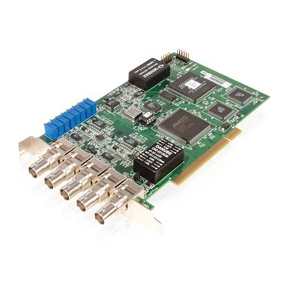
- Page 1 NuDAQ PCI-9812/10 20MHz Simultaneous 4-CH Analog Input Card Users’ Guide...
- Page 2 @Copyright 1997~2000 ADLink Technology Inc. All Rights Reserved. Manual Rev. 2.24: April 10, 2000 The information in this document is subject to change without prior notice in order to improve reliability, design and function and does not represent a commitment on the part of the manufacturer.
- Page 3 Getting service from ADLink ♦ Customer Satisfaction is always the most important thing for ADLink Tech Inc. If you need any help or service, please contact us and get it. ADLink Technology Inc. Web Site http://www.adlink.com.tw Sales & Service service@adlink.com.tw Technical NuDAQ nudaq@adlink.com.tw...
- Page 5 CONTENTS How to Use This Guide .......... iv Chapter 1 Introduction........... 1 Features................1 Applications..............2 Specifications ..............2 Software Support............4 1.4.1 Programming Library..............4 ® 1.4.2 PCIS-LVIEW: LabVIEW Driver..........4 1.4.3 PCIS-VEE: HP-VEE Driver............4 1.4.4 DAQBench : ActiveX Controls ..........5 1.4.5 DASYLab PRO................5...
- Page 6 FIFO Control Register........... 22 4.10 Acquisition Enable Register ......... 22 4.11 Clock Source Register..........23 4.12 High Level Programming..........24 4.13 Low Level Programming..........24 Chapter 5 Operation Theorem ......25 A/D Conversion Procedure ........... 25 A/D Signal Source Control ..........26 A/D Trigger Source Control ..........
- Page 7 6.13 W_9812_Get_Sample............ 50 Chapter 7 Calibration ...........51 What you need.............. 51 VR Assignment ............. 52 A/D Calibration.............. 52 7.3.1 AD Calibration for Channel 0 ..........52 7.3.2 AD Calibration for Channel 1,2,3........... 52 Chapter 8 Software Utility........55 Running 9812util.exe ............ 56 System Configuration ...........
- Page 8 How to Use This Guide This manual is designed to help you use the PCI-9812/10. The manual describes how to modify various settings on the PCI- 9812/10 card to meet your requirements. It is divided into eight chapters: • Chapter 1, "Introduction", gives an overview of the product features, applications, and specifications.
-
Page 9: Chapter 1 Introduction
Introduction PCI-9812/10 is an advanced-perform ance data acquisition card based on 32-bit PCI Bus architecture. The maximum sampling rate of PCI- 9812/10 is up to 20M samples per second, With an emphasis on continuous, non-stop, high-speed, streaming of A/D samples to host memory. -
Page 10: Applications
Applications • IF and BASEBAND Digitization • Ultrasound Imaging • Gamma Cameras • Test Instrument • CCD Imaging • Video Digitizing Specifications ♦ Analog Input (A/D) • Converters: B.B. ADS800 series • Input Channels: 4 single-ended • Resolution: 12-bit (9812), 10-bit (9810) •... - Page 11 • A/D Clock Sources: Internal clock, Continuous external digital clock and Continuous external sine wave. • Input Impedance of External Clock Source: 50Ω • Trigger Sources: Software, Analog threshold comparator using internal D/A to set trigger level, and External digital trigger •...
-
Page 12: Software Support
Software Support ADLink provides versatile software drivers and packages for users’ different approach to built-up a system. We not only provide programming library such as DLL for many Windows systems, but also ® provide drivers for many software package such as LabVIEW , HP , DASYLab , InTouch... - Page 13 interface with HP VEE software package. PCIS-VEE supports Windows 95/98/NT. The HP-VEE drivers are free shipped with the board. You can install and use them without license. For detail information about PCIS-VEE, please refer to the user’s guide in the (\\Manual_PDF\Software\PCIS-VEE) 1.4.4 DAQBench...
-
Page 14: Chapter 2 Installation
Installation This chapter describes how to install the PCI-9812/10. Firstly, please read the contents in the package and unpacking information and following these instructions carefully. The PCI-9812/10 will perform an automatic configuration of the IRQ and I/O port address. There is no need to set any configuration, as you would use in an ISA form factor DAS card. -
Page 15: What You Have
What You Have In addition to this User's Guide, the package includes the following items: w PCI-9812/10 Enhanced Multi-function Data Acquisition Card w 5 BNC terminators w ADLink All-in-one CD w Software Installation Guide If any of these items is missing or damaged, contact the dealer from whom you purchased the product for replacement. -
Page 16: Pci-9812/10'S Layout
PCI-9812/10's Layout C05V C0LO C25V C05V C2LO C0LO Figure 2.1 PCB Layout of the PCI-9812/10 8 • Installation... -
Page 17: Hardware Installation
Hardware Installation Outline PCI configuration The PCI cards (or CompactPCI cards) are equipped with plug and play PCI controller, it can request base addresses and interrupt according to PCI standard. The system BIOS will install the system resource based on the PCI cards’ configuration registers and system parameters (which are set by system BIOS). -
Page 18: Chapter 3 Signal Connection
Signal Connection This chapter describes the connector of the PCI-9812/10, the signal connection between the PCI-9812/10 and external devices, and the switch setting for different applications. Connectors The PCI-9812/10 connects to external devices through five BNC connectors and one 10-pin dual-in-line header. Fig. 3.1 shows the location of these connectors. - Page 19 • J1 : The J1 BNC connector is used for the input signal of channel 0 A/D converter. • J2 : The J2 BNC connector is used for the input signal of channel 1 A/D converter. • J3 : The J3 BNC connector is used for the input signal of channel 2 A/D converter.
-
Page 20: Analog Input Impedance Setting
Analog Input Impedance Setting This section describes the characteristics of the different inputs of the PCI-9812/10. 3.2.1 Analog Input PCI-9812/10 has four analog input channels which are connected through connectors J1 ~ J4. The input impedance and input amplitude range can be changed through soldering the gap switches on board (refer to PCI-9812/10’s layout). -
Page 21: External Clock 0
The corresponding switches and resistors of other channels are shown below: Channel Switches Resistor Channel 0 C0LO C05V Channel 1 C1LO C15V Channel 2 C2LO C25V Channel 3 C3LO C35V 3.2.2 External Clock 0 The external clock 0 (J5) is a sine wave signal which is converted to a TTL signal inside the PCI-9812/10. -
Page 22: Chapter 4 Registers Format
Registers Format The detailed descriptions of the register form at and structure of the PCI-9812/10 are specified in this chapter. This information is useful for the programmer who wants to handle the card using low-level programming. I/O Port Address The PCI-9812/10 functions as 32-bit PCI target device to any master on the PCI bus. -
Page 23: Adc Channel Enable Register
ADC Channel Enable Register The PCI-9812/10 has 4 analog input channels, named CH0, CH1, CH2, and CH3. CH0 ~ CH3 can be enabled or disabled by bit 0 ~ 3 of the ADC channel enable register. Address: BASE + 0 Attribute: write only Data Format: BASE+0... -
Page 24: Adc Clock Divisor Register
ADC Clock Divisor Register The ADC sampling clock is generated by feeding the ADC source clock to a clock frequency divider, the output of the frequency divider becomes the sampling clock. The frequency of the ADC sampling clock is: Frequency of source clock / ADC clock divisor Address: BASE + 04h Attribute: write only Data Format:... -
Page 25: Trigger Mode Register
Trigger Mode Register The PCI-9812/10 has five trigger modes: software trigger, post trigger, pre-trigger, middle trigger and delay trigger. The trigger mode register is used to specify which trigger mode is currently used. Address: BASE + 08h Attribute: write only Data Format: Base + 8 TRGMOD2... -
Page 26: Trigger Level Register
Trigger Level Register The trigger condition of the PCI-9812/10 includes trigger level and trigger slope. This register sets the trigger level, and the trigger source register described in the next paragraph sets the trigger slope. Address: BASE + 0ch Attribute: write only Data Format: BASE+Ch TRGLVL7 TRGLVL6 TRGLVL5 TRGLVL4 TRGLVL3 TRGLVL2 TRGLVL1 TRGLVL0 BASE+Dh... -
Page 27: Trigger Source Register
Trigger Source Register PCI-9812/10 supports five trigger sources. They are CH0, CH1, CH2, CH3 and external digital trigger. Address: BASE + 10h Attribute: write only Data Format: Base + 10 TRGSLP TRGSRC2 TRGSRC1 TRGSRC0 Base + 11 Base + 12 Base + 13 TRGSLP: trigger slope. -
Page 28: Post Trigger Counter Register
Post Trigger Counter Register The post trigger counter is a 16-bit down counter. The counter is pre-loaded with the value in post trigger counter register and it will count down on the rising edge of ADC sampling clock after the trigger condition is met. -
Page 29: Fifo Status Register
FIFO Status Register This register is used to monitor some status of the PCI-9812/10. Address: BASE + 18h Attribute: read Data Format: BASE+18h PTCO FIFOOR FIFOHF FIFOIR BASE+19h BASE+1Ah BASE+1Bh bit 0 -- FIFOIR, FIFO input ready flag. 0: The FIFO is not ready for input, which means the FIFO is full 1: The FIFO is ready for input (not full). -
Page 30: Fifo Control Register
FIFO Control Register This register is used to control the on-board FIFO memory. Address: BASE + 18h Attribute: write Data Format: BASE+18h CLRTRG CLRFIFO BASE+19h BASE+1Ah BASE+1Bh bit 0 -- CLRFIFO, clear the on-board FIFO When a "1" is written to this bit, the entire on-board FIFO is cleared. -
Page 31: Clock Source Register
4.11 Clock Source Register The register is used to select the system clock source. Address: BASE + 20h Attribute: write only Data Format: BASE+18h CLKSRC1 CLKSRC0 Freq_Sel BASE+19h BASE+1Ah BASE+1Bh bit 31..3 -- don't care bit 2..1 -- CLKSRC1..0, ADC clock source bit 0: --- Freq_Sel, Frequency selection. -
Page 32: High Level Programming
4.12 High Level Programming To operate the PCI-9812/10, you can by-pass the detailed register structures and control your PCI-9812/10 card directly via the high-level Application-Programming-Interface (API). The software Libraries, including DOS Library for Borland C++ and DLL driver for Win-95, are included in the ADLink’s “All-in-one CD”. -
Page 33: Chapter 5 Operation Theorem
Operation Theorem The operation theorem of the functions on PCI-9812/10 card is described in this chapter. The functions include A/D conversion and digital input. The operation theorem will help you to understand, opesate and program the PCI-9812/10. A/D Conversion Procedure Before programming the PCI-9812/10 to perform the A/D conversions, you have to understand the following concepts: A/D conversion procedure... -
Page 34: A/D Signal Source Control
After deciding the A/D siginal source, users must decide how to trigger the A/D conversion and define/control the trigger source. The A/D converter will start to convert the siginal to a digital value when a trigger condition is met. The PCI-9812/10 provides five trigger modes, please refer to section 5.3 The A/D clock is controlled by internal clock or external clock source. -
Page 35: A/D Trigger Source Control
A/D Trigger Source Control Performing the trigger acquisition in PCI-9812/10, the following items have to be specified before DMA operation starts: clock source: refer to section 5.4 clock rate: refer to section 5.4 trigger source: refer to section 5.3.1. trigger level: The trigger event occurs when the trigger signal crosses the specified trigger voltage. -
Page 36: Simultaneous Trigger For Multiple Cards
Positive-slope trigger event occurs Negative-slope trigger event occurs Level +0.5V External Digital Trigger An external digital trigger occurs when a rising edge or a falling edge is detected on the digital signal connected to pin3 of JP1 for external digital trigger. Positive-edge Negative-edge trigger trigger event... -
Page 37: Trigger Modes
5.3.3 Trigger Modes Software-Trigger Acquisition This trigger mode does not need any external trigger source. The trigger event occurs when you call _9812_AD_DMA_Start( ) function to start the operation. Post-Trigger Acquisition Use post-trigger acquisition in applications when you want to collect data after a specified trigger event. - Page 38 Middle-Trigger Acquisition Use middle-trigger acquisitions in application where you want to collect data before and after a specified trigger event. Acquiring data before a trigger event occurs for Middle trigger might not get the specified count of data, just like the pre-trigger mode. DMA start External trigger Event DMA Stop...
-
Page 39: A/D Clock Source Control
A/D Clock Source Control The AD clock source determines how the board regulates the timing of conversions when you are acquiring multiple samples from a single channel or from a group of multiple channels. The A/D clock sources on the PCI-9812 must use pacer clock but not single shot, because the A/D converters are in a pipelined structure, which needs 8 conversion clock to complete the conversion of digital data. -
Page 40: Multiple Cards Operation
Sampling Rate = Frequency of Source Clock / ADC Clock Divisor Note: 1.The clock divider must be an even number, that is, the ADC Clock Divisor = 2, 4, 6, 8, 10… 1024 (maximum), The minimum divider value is 2.Please refer to section 6.2.6 and section 6.2.7 to set the clock source and frequency divider. -
Page 41: A/D Data Transfer
A/D Data Transfer 5.5.1 AD Data Transfer For acquiring the AD data, there are several function blocks on the PCI-9812 board. Even when the maximum sampling rate is specified up to 20MHz, however, there are some limitations due to the high total data throughput. Users should refer to the following block diagram to understand how the analog signal is converted to digital form and transferred to PC host memory. -
Page 42: Total Data Throughput
5.5.3 Total Data Throughput When 4 channels start at the same time, the total data throughput from the AD converter to the on-board FIFO memory will be Sampling Rate x number of channels x 2 bytes/channel. Therefore, the maximum total data throughput is 160M bytes /sec. 160MB/s = 20MHz ×... -
Page 43: Host Memory Operation
Bus-mastering DMA provides the fastest data transfer rate on PCI- bus. Once the analog input operation starts, control returns to your program. The hardware temporarily stores the acquired data in the onboard A/D FIFO and then transfers the data to a user-defined DMA buffer memory in the computer. -
Page 44: Summary
5.5.7 Summary So far we have discussed the A D data transferring, the maximum sampling rate and the maximum continuous data length at the sample time. Here we summarize to get the following steps: 1. caculate the total data throughput; 2. - Page 45 A/D Data (Hex) Decimal Value V (Volts, -1V~1V) V (Volts, -5V~5V) 7FC 0 +32704 +1.0000 +5.0000 400 0 +16384 +0.5002 +2.5010 0040 +0.0005 +0.0025 000 0 0.0000 0.0000 FFC 0 -0.0005 -0.0025 C00 0 -16384 -0.5002 -2.5010 804 0 -32704 -1.0000 -5.0000 800 0...
-
Page 46: Chapter 6 C/C++ Library
C/C++ Library This chapter describes the software library for operating this card. Only the functions in DOS library and Windows 95 DLL are described. Please refer to the PCIS-DASK function reference manual, which included in ADLINK CD, for the descriptions of the Windows 98/NT/2000 DLL functions. -
Page 47: Programming Guide
Programming Guide 5.2.1 Naming Convention The functions of the NuDAQ PCI cards or NuIPC CompactPCI cards’ software driver are using full-names to represent the functions' real meaning. The naming convention rules are: In DOS Environment : _{hardware_model}_{action_nam e}. e.g. _9812_Initial(). functions PCI-9812 driver... -
Page 48: Initial
_9812_Initial @ Description This function is used to initialize PCI-9812/10. Every PCI-9812/10 has to be initialized by this function before calling other functions. @ Syntax C/C++ (DOS) int _9812_Initial (int card_number, U16 *op_base_address,U16 *pt_base_address, U16 *irq_no, U16 *pci_master) C/C++ (Windows 95) int W_9812_Initial (int card_number, U16 *op_base_address,U16 *pt_base_address, U16 *irq_no, U16 *pci_master) -
Page 49: Close
_9812_Close @ Description This function is used to close a previously initialized 9812 card. @ Syntax C/C++ (DOS) int _9812_Close (int card_number) C/C++ (Windows 95) int W_9812_Close (int card_number) Visual Basic (Windows 95) W_9812_Close (ByVal card_number As Long) As Long @ Argument card_number: the card number of PCI-9812 to be closed, the... - Page 50 card_number:the card number of PCI-9812 ch_cnt: number of A/D channel enabled. The valid values are: 0: no channel is enabled 1: only channel 0 is enabled 2: channel 0, 1 are enabled, and the sequence of channel scan is 0, 1, 0, 1, …….. 4: all channels are enabled, and the sequence of channel scan is 0, 1, 2, 3, 0, 1, 2, 3, …..
-
Page 51: Ad_Dma_Status
_9812_AD_DMA_Status @ Description Since the _9812_AD_DMA_Start is executed on background, you can issue the function _ 9812_AD_DMA_Status to check its operation status. @ Syntax C/C++ (DOS) int _9812_AD_DMA_Status(int card_number, int *status, U32 *start_idx) C/C++ (Windows 95) int W_9812_AD_DMA_Status(int card_number, int *status, U32 *start_idx) Visual Basic (Windows 95) W_9812_AD_DMA_Status (ByVal card_number As Long,... -
Page 52: Ad_Dma_Stop
_9812_AD_DMA_Stop @ Description This function is used to stop the DMA data transfer. After executing this function, the _9812_AD_DMA_Start function stops. The function returns the number of data that has been transferred, no matter if the A/D DMA data transfer is stopped by this function or by the DMA terminal count ISR. -
Page 53: Set_Clk_Rate
@ Argument card_number:the card number of PCI-9812/10 to be selected clk_src : the ADC clock source, the valid values are as follows: 0: INT_CLK: internal clock 1: SIN_CLK: external sin wave clock 2: SQR_CLK: external square clock ftpci : Frequency selection. AD2_GT_PCI: the frequency of A/D clock source is higher than PCI clock frequency. -
Page 54: Set_Trig
6.10 _9812_Set_Trig @ Description This function is used to set up a trigger. The function specifies the trigger mode, trigger level (voltage), trigger source, trigger slope and post trigger count. Please refer to section 4.4~4.7 for the detailed description of trigger setting. @ Syntax C/C++ (DOS) int _9812_Set_Trig (int card_number, int... - Page 55 trig_lvl: trigger level. The relationship between the 8 -bit trigger level and the trigger voltage is shown in section 4.5. C/C++ Library • 47...
-
Page 56: W_9812_Alloc_Dma_Mem
post_trig_cnt:The post trigger count. This v alue is preloaded to the post trigger counter when the post trigger counter register is written. It will count down on the rising edge of ADC sampling clock after the trigger condition is met. When the count reaches 0, the counter stops. - Page 57 C/C++ Library • 49...
-
Page 58: W_9812_Free_Dma_Mem
6.12 W_9812_Free_DMA_Mem @ Description Release a system DMA memory under Windows 95 environment. This function is only available in Windows 95 version. @ Syntax C/C++ (Windows 95) int W_9812_Free_DMA_Mem (HANDLE memID) Visual Basic (Windows 95) W_9812_Free_DMA_Mem (ByVal memID As Long) As Long @ Argument memID: The memory ID of the system DMA memory to... -
Page 59: Chapter 7 Calibration
Calibration In data acquisition, calivrating your measurement devices to maintain the accuracy is very important. Users can calibrate the analog input and analog output channels under the users' operating environment to optimize the accuracy. This chapter will guide you to calibrate your PCI-9812/10 to an accurate condition. -
Page 60: Vr Assignment
VR Assignment There are eight variable resistors (VR) on the PCI-9812/10 board to allow you to make accurate adjustments on A/D channels. The function of each VR is specified in Table 7.1. A/D channel 0 offset adjustment A/D channel 1 offset adjustment A/D channel 2 offset adjustment A/D channel 3 offset adjustment A/D channel 0 full scale adjustment... - Page 61 Calibration • 53...
- Page 62 A calibration utility is provided in the software CD included in the product package. The detailed calibration procedures and description can be found in the utility. Users only need to run the software calibration utility and follow the procedures. You will get the accurate measurement data.
-
Page 63: Chapter 8 Software Utility
Software Utility The software CD provides a utility program, 9812util.exe. This program has three functions, System Configuration, Calibration, and Functional Testing. This utility is designed as menu-driven based windowing style, that is, it provides not only the text messages for operating guidance, but also graphics to instruct you how to set hardware configuration correctly. -
Page 64: Running 9812Util.exe
****** PCI-9812/10 Utility Rev. 1.0 ****** Copyright © 1995-1997, ADLink Technology Inc. All rights reserved. <F1> : Configuration. -
Page 65: System Configuration
System Configuration This function will guides you to configure the PCI-9812/10 card, and set the right hardware configuration. The configuration window shows the setting items that you have to set before using the PCI- 9812/10 card. The following diagram will be displayed on the screen as you choose the Configuration function from main menu. -
Page 66: Calibration
Calibration This function will guide you on how to calibrate the PCI-9812/10. The calibration program serves as a useful test for the PCI- 9812/10's A/D,D/A and DIO functions and can aid in troubleshooting if problems arise. Note : For an environment with frequent large changes in temperature vibration, recalibration interval,... - Page 67 For example, if you select 3, the following figure will be displayed on the screen: Software Utility • 59...
-
Page 68: Functional Testing
Functional Testing This function is used to test the functions of PCI-9812/10 A/D. When you choose testing function from the main menu list, a function testing test window is displayed on the screen. following is the figure of function testing window. The message shown at the bottom indicates how to change the setting of trigger mode, trigger signal polarity, trigger level, channel number and post trigger count (for middle trigger and delay trigger). - Page 69 Software Utility • 61...
-
Page 70: Product Warranty/Service
Product Warranty/Service Seller warrants that equipment furnished will be free from defects in material and workmanship for a period of one year from the confirmed date of purchase of the original buyer and that upon written notice of any such defect, Seller will, at its option, repair or replace the defective item under the terms of this warranty, subject to the provisions and specific exclusions listed herein.
Need help?
Do you have a question about the NuDAQ PCI-9812/10 and is the answer not in the manual?
Questions and answers