
Related Manuals for ADLINK Technology PCI-9524


Summary of Contents for ADLINK Technology PCI-9524
- Page 1 PCI-9524 24-Bit Precision Load Cell Input Card User’s Manual Manual Revision: 2.00 Revision Date: April 09, 2008 Part No: 50-11236-1000 Advance Technologies; Automate the World.
-
Page 2: Revision History
PCI-9524 ADLINK Technology, Inc. User’s Manual Copyright 2008 Revision History Revision Release Date Description of Change(s) Document Created 2.00 2008/04/09 Initial Release... -
Page 3: Preface
Environmental Responsibility ADLINK is committed to fulfill its social responsibility to global environmental preservation through compliance with the Euro- pean Union's Restriction of Hazardous Substances (RoHS) direc- tive and Waste Electrical and Electronic Equipment (WEEE) directive. - Page 4 PCI-9524 ADLINK Technology Inc. User’s Manual Copyright 2008 ® ® ® ® 98, Windows NT, Windows 2000, Windows XP, and Windows ® ® Vista are registered trademarks of Microsoft Corporation. PCI™, is a registered trademark of the Peripheral Component Interconnect Special Interest Group (PCI-SIG).
-
Page 5: Using This Manual
Copyright 2008 User’s Manual Using this Manual Audience and Scope The PCI-9524 User’s Manual is intended for hardware technicians and systems operators with knowledge of installing, configuring and operating industrial grade PCI cards. Manual Organization This manual is organized as follows:... -
Page 6: Conventions
PCI-9524 ADLINK Technology Inc. User’s Manual Copyright 2008 Conventions Take note of the following conventions used throughout this manual to make sure that users perform certain tasks and instructions properly. Additional information, aids, and tips that help users per- form tasks. -
Page 7: Acronyms & Terminology
ADLINK Technology Inc. PCI-9524 Copyright 2008 User’s Manual Acronyms & Terminology The following terms are used throughout this document. This list is prepared in alphabetical order for clarity. A/mA - (Ampere/amp/milliampere) a unit of electric current, or amount of electric charge per second... - Page 8 PCI-9524 ADLINK Technology Inc. User’s Manual Copyright 2008 EMI - Electromagnetic Interference ENOB - Effective Number of Bits FIFO - First In, First Out FPGA - Field-Programmable Gate Array GB - Gigabyte (1,073,741,824 bytes) Hz/KHz/MHz - hertz / Kilo hertz / Mega hertz, standard unit of...
- Page 9 ADLINK Technology Inc. PCI-9524 Copyright 2008 User’s Manual TBD - To Be Determined TTL - Transistor-Transistor Logic, digital circuits built from bipolar junction transistors and resistors. V/mV/µV - Volt / milli Volt / micro Volt, a derived unit of electrical...
-
Page 10: Reference Documentation
The following list of documents may be used as reference materi- als to support installation, configuration and/or the operation of the PCI-9524. This list is prepared in alphabetical order (by vendor/ organization name, then by document title) for clarity. Vendor(s) Title Rev. -
Page 11: Getting Service
Toll-Free: +1-866-4 ADLINK Fax No.: +1-949-727-2099 Mailing Address: 8900 Research Drive, Irvine, CA 92618, USA ADLINK TECHNOLOGY CO. LTD. (BEIJING) Sales & Service: market@adlinktech.com Telephone No.: +86-10-5885-8666 Fax No.: +86-10-5885-8625 Mailing Address: Rm. 801, Power Creative E, No. 1, B/D Shang Di East Rd. - Page 12 Telephone No.: +65-6844-2261 Fax No.: +65-6844-2263 Mailing Address: 84 Genting Lane #07-02A, Cityneon Design Center, Singapore 349584 ADLINK TECHNOLOGY SINGAPORE PTE. LTD. (INDIA Liaison Office) Sales & Service: india@adlinktech.com Telephone No.: +91-80-6560-5817 Fax No.: +91-80-2244-3548 Mailing Address: No. 1357, Ground Floor, "Anupama",...
-
Page 13: Table Of Contents
PCI-9524 Copyright 2008 User’s Manual Table of Contents PCI-9524..................i Revision History..............ii Preface ..................iii Copyright 2008 ADLINK TECHNOLOGY INC....iii Disclaimer ...............iii Environmental Responsibility ..........iii Trademarks ..............iii Using this Manual ............v Conventions ..............vi Acronyms & Terminology ..........vii Reference Documentation .......... - Page 14 3.3.4 Interfacing Isolated DO with External Loads....... 43 3.3.5 Interfacing Isolated DI with External Devices...... 45 4 Operation Theory .............. 47 PCI-9524 Function Diagram ..........47 Analog Input Channels............48 4.2.1 Signal Acquisition and Processing Flow ......48 4.2.2 How to Define a 1 in 200,000 Count Resolution ....49 4.2.3 Data Rate versus Sampling Rate........
- Page 15 ADLINK Technology Inc. PCI-9524 Copyright 2008 User’s Manual 4.6.1 Isolated Digital Inputs ............70 4.6.2 Isolated Digital Outputs............70 Trigger Sources ..............70 4.7.1 Software-Trigger ..............70 4.7.2 External Digital Trigger ............70 4.7.3 Pulse Comparator Trigger ..........71 4.7.4 Position Comparator Trigger..........72 5 Calibration.................
- Page 16 PCI-9524 ADLINK Technology Inc. User’s Manual Copyright 2008 This page intentionally left blank. Table of Contents...
-
Page 17: List Of Figures
Figure 1-9: Frequency Response Sampling at 15,000 SPS .... 12 Figure 1-10: Frequency Response Sampling below 15,000 SPS ..13 Figure 2-1: PCI-9524 PCB Layout and Mechanical Drawing ... 23 Figure 3-1: CN1 Connector & Pin Assignments....... 27 Figure 3-2: CN2 Connector & Pin Assignments....... 29 Figure 3-3: SSI Connector &... - Page 18 Figure 3-17: Connecting to a low-side push button......45 Figure 3-18: Connecting to an external sink driver ......46 Figure 4-1: PCI-9524 Function Diagram .......... 47 Figure 4-2: Signal acquisition and data processing flow for transducer input channels ........48 Figure 4-3: SINC Filter Power Line Noise Rejection at 60 Hz Multiples ............
- Page 19 ADLINK Technology Inc. PCI-9524 Copyright 2008 User’s Manual List of Tables Table 1-1: -3dB small signal bandwidth: (Typical, 25°C) ....4 Table 1-2: System Noise (including Quantization, Typical, 25°C) ..4 Table 1-3: Transducer Input Impedance........... 5 Table 1-4: Transducer CMRR (DC to 60 Hz, Typical 25°C) ..... 5 Table 1-5: Settling Error: (Typical, 25°C) ..........
- Page 20 PCI-9524 ADLINK Technology Inc. User’s Manual Copyright 2008 This page intentionally left blank. List of Tables...
-
Page 21: Introduction
DAQ card capable of up to 30 kS/s sampling rate, providing 4-CH load-cell transducer input channels, and 4-CH general purpose analog input. In addition, the PCI-9524 comes with a 2-CH 16-bit analog output, isolated motion I/O and digital I/O. The highly inte- grated function makes the PCI-9524 the ideal solution for com- bined data acquisition and motion control functionalities. -
Page 22: Features
PCI-9524 ADLINK Technology Inc. User’s Manual Copyright 2008 1.1 Features PCI-9524 24-bit multifunction DAQ card provides the following advanced features: Supports 32-bit 3.3V or 5V PCI bus Load-cell transducer input channels 4-CH differential analog input with remote-sense 4-CH transducer excitation, 10V or 2.5V selectable... -
Page 23: Specifications
ADLINK Technology Inc. PCI-9524 Copyright 2008 User’s Manual 1.3 Specifications Analog Input (AI) for Transducers Number of channels: (programmable) 4 differential inputs (DI) A/D converter: ADS1255 Maximum sampling rate: Without Auto-zero 30,000 samples/s (single channel) 1,638 samples/s (multiplexed/scanning) With Auto-zero... -
Page 24: Table 1-1: -3Db Small Signal Bandwidth: (Typical, 25°C)
PCI-9524 ADLINK Technology Inc. User’s Manual Copyright 2008 Remote-sense inputs: Power on: -40V to +55V (continuous) Power off: -40V to +55V (continuous) FIFO buffer size: 1024 samples (1024 x 32 bits) Data transfers: Programmed I/O Bus-mastering DMA with scatter/gather Table 1-1: -3dB small signal bandwidth: (Typical, 25°C) -
Page 25: Table 1-3: Transducer Input Impedance
ADLINK Technology Inc. PCI-9524 Copyright 2008 User’s Manual System Data Peak Peak Input Res. in RMS Res Noise in Rate in Res. in Res. in Range Bits in µV Bits µV (ENOB) 20.1 17.1 0.101 0.742 19.6 16.4 0.146 1.113 19.2... -
Page 26: Table 1-5: Settling Error: (Typical, 25°C)
PCI-9524 ADLINK Technology Inc. User’s Manual Copyright 2008 Table 1-5: Settling Error: (Typical, 25°C) Input Range Condition Settling Error ±200mV Scanning 200mV step max 0.01% Time-base source: Internal 40 MHz Trigger mode: post-trigger Offset error: Before calibration: ±0.5mV typical After calibration: ±0.001mV typical (auto-zero disabled), <... -
Page 27: Table 1-6: Programmable Input Range And Gain
ADLINK Technology Inc. PCI-9524 Copyright 2008 User’s Manual Table 1-6: Programmable input range and gain Bipolar Input Range Gain ±10V ±5V ±2.5V ±1.25V Operational common-mode input range: ±13V Overvoltage protection: Power on: ±30V (continuous) Power off: ±15V (continuous) FIFO buffer size: 1024 samples (1024 x 32 bits) -
Page 28: Table 1-8: -3Db Small Signal Bandwidth Vs. Sampling Rates, In ±10V Range
PCI-9524 ADLINK Technology Inc. User’s Manual Copyright 2008 Table 1-8: -3dB small signal bandwidth vs. sampling rates, in ±10V range Sampling Rate In Samples-per-second Bandwidth (-3 dB) (SPS) 1.1 Hz 2.2 Hz 4.4 Hz 6.6 Hz 11 Hz 13 Hz... -
Page 29: Figure 1-2: Effective-Number-Of-Bits Vs. Gain
ADLINK Technology Inc. PCI-9524 Copyright 2008 User’s Manual System Noise (LSBrms, including Quantization, Typical, 25ºC) Figure 1-2: Effective-number-of-bits vs. Gain ENOB vs PGA Gain [Input = AGND] 1000 2000 3750 7500 15000 30000 Sam pling Rate [Sam ples per Second]... -
Page 30: Figure 1-4: Spectral Response ±10V Range, 0.996094 Hz Sine Wave, -1 Db Fs
PCI-9524 ADLINK Technology Inc. User’s Manual Copyright 2008 Spectral Response (At 30,000-SPS, Typical, 25ºC) Spectral Response Figure 1-4: ±10V range, 0.996094 Hz sine wave, -1 dB FS Input Signal = 996.094 Hz @ -1 dBFS, Sampling rate = 30 KHz SINAD = 99.5171 dB... -
Page 31: Figure 1-6: Spectral Response ±2.5V Range, 0.996094 Hz Sine Wave, -1 Db Fs
ADLINK Technology Inc. PCI-9524 Copyright 2008 User’s Manual Spectral Response Figure 1-6: ±2.5V range, 0.996094 Hz sine wave, -1 dB FS Input Signal = 996.094 Hz @ -1 dBFS, Sampling rate = 30 KHz SINAD = 97.5555 dB SNR = 98.0951 dB THD = -106.8792... -
Page 32: Figure 1-8: Frequency Response Sampling At 30,000 Sps
PCI-9524 ADLINK Technology Inc. User’s Manual Copyright 2008 Frequency Response (vs. normalized sampling frequencies): Frequency Response Figure 1-8: Sampling at 30,000 SPS Frequency Response versus Norm. Sampling Frequency -100 -120 0.00 0.17 0.33 0.50 0.67 0.83 1.00 Normalized Sampling Frequency (Fs) -
Page 33: Figure 1-10: Frequency Response Sampling Below 15,000 Sps
ADLINK Technology Inc. PCI-9524 Copyright 2008 User’s Manual Frequency Response Figure 1-10: Sampling below 15,000 SPS Frequency Response versus Norm. Sampling Frequency -100 -120 0.00 0.17 0.33 0.50 0.67 0.83 1.00 Normalized Sampling Frequency (Fs) Table 1-9: General Purpose Input Impedance... -
Page 34: Table 1-11: Settling Error: (Typical, 25ºc)
PCI-9524 ADLINK Technology Inc. User’s Manual Copyright 2008 Table 1-11: Settling Error: (Typical, 25ºC) Input Range Condition Settling Error ±10V Scanning 20Vpp <0.0005% ±5V Scanning 10Vpp <0.0005% ±2.5V Scanning 5Vpp <0.0005% ±1.25V Scanning 2.5Vpp <0.0005% Time-base source: Internal 40 MHz... - Page 35 ADLINK Technology Inc. PCI-9524 Copyright 2008 User’s Manual Analog Output (AO) Number of channels: 2 analog voltage outputs D/A converter: DAC8812 Maximum update rate: 10K sample/s Resolution: 16-bit Data transfers: Programmed I/O Output range: ±10V (after software calibration) Settling time (0.1% of full scale): 2 µs Slew rate: 15V/µS...
- Page 36 PCI-9524 ADLINK Technology Inc. User’s Manual Copyright 2008 Isolated Pulse Command Outputs Number of channels: 3 Output type: AM26LS31 differential line-driver Compliant to ANSI TIA/EIA-422-B and ITU Recommenda- tion V.11 standards Logic Compatibility: 5V TTL with complementary output Output voltage: Logic low: VOL = 0.5V max.;...
- Page 37 ADLINK Technology Inc. PCI-9524 Copyright 2008 User’s Manual Isolated Digital Inputs Number of channels: 8 Input type: Bipolar, resistive differential Input impedance: 2.7K- Ω || 250-pF Input voltage: Logic low: VIL = 0.7V max. Logic high: VIH = 4.8V min.
- Page 38 PCI-9524 ADLINK Technology Inc. User’s Manual Copyright 2008 Isolated Power Supplies Number of channels: 2 Nominal output voltage ISO5VDD: 5V ±0.05V ISOPWR: 5V ±0.15V Output current (Pulse Command channels are unused) ISO5VDD: 160mA max. ISOPWR: 16mA max. Maximum output current (n...
-
Page 39: Software Support
Contact your ADLINK dealers if you want to purchase the software license. Programming Library For customers who want to write their own programs, ADLINK pro- vides the PCIS-DASK function library that is compatible with vari- ous operating systems. - Page 40 PCI-9524 ADLINK Technology Inc. User’s Manual Copyright 2008 This page intentionally left blank. Introduction...
-
Page 41: Getting Started
ADLINK Technology Inc. PCI-9524 Copyright 2008 User’s Manual Getting Started This chapter further describes the PCI-9524; a proper installation environment, its package contents and basic information users should be aware of. 2.1 Installation Environment Whenever unpacking and preparing to install any equipment described in this manual, please refer to the Important Safety Instructions chapter of this manual. -
Page 42: Package Contents
2.2 Package Contents Before continuing, check the package contents for any damage and check if the following items are included in the packaging: PCI-9524 Multi-function Data Acquisition Card ADLINK All-in-one Compact Disc Software Installation Guide PCI-9524 User’s Manual If any of these items are missing or damaged, contact the dealer from whom you purchased the product. -
Page 43: Adlink Technology Inc. Pci
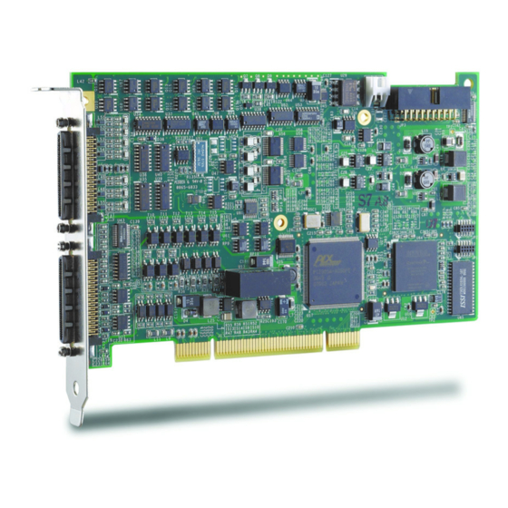
ADLINK Technology Inc. PCI-9524 Copyright 2008 User’s Manual 2.3 PCI-9524 Layout Figure 2-1: PCI-9524 PCB Layout and Mechanical Drawing Controller Getting Started... -
Page 44: Installing The Card
PCI-9524 ADLINK Technology Inc. User’s Manual Copyright 2008 2.4 Installing the Card To install the card: 1. Turn off the system/chassis and disconnect the power plug from the power source. 2. Remove the system/chassis cover. 3. Select the PCI slot that you intend to use, then remove the bracket opposite the slot, if any. -
Page 45: Pci Configuration
These system parameters are determined by the installed drivers and the hardware load rec- ognized by the system. Users can use the PCI_SCAN software utility on the ADLINK All-in-One CD to read/check the system configuration. 2. Configuration: The board configuration is done on a board-by-board basis for all PCI boards on your system. - Page 46 PCI-9524 ADLINK Technology Inc. User’s Manual Copyright 2008 This page intentionally left blank. Getting Started...
-
Page 47: Signal Connections
PCI-9524 Copyright 2008 User’s Manual Signal Connections This chapter describes the connectors of PCI-9524, and the signal connections between PCI-9524 and external devices. Please see Figure 3-1, Figure 3-2 and Figure 3-3 for details. CN1/CN2 - 68-pin VHDCI Connector SSI - SSI Connector 3.1 Connectors &... - Page 48 PCI-9524 ADLINK Technology Inc. User’s Manual Copyright 2008 Pin # Pin # AIH4 AIL4 AIH5 AIL5 AIH6 AIL6 AIH7 AIL7 AGND AGND AGND AGND AGND AGND AGND AGND AGND AGND AGND AGND AGND AGND AGND AGND AGND AGND AGND AGND...
-
Page 49: Figure 3-2: Cn2 Connector & Pin Assignments
ADLINK Technology Inc. PCI-9524 Copyright 2008 User’s Manual Figure 3-2: CN2 Connector & Pin Assignments Pin # Pin # AI0+ AI0- VEX0+ VEX0- VEX_SEN0+ VEX_SEN0- AI1+ AI1- VEX1+ VEX1- VEX_SEN1+ VEX_SEN1- AI2+ AI2- VEX2+ VEX2- VEX_SEN2+ VEX_SEN2- AI3+ AI3- VEX3+... - Page 50 PCI-9524 ADLINK Technology Inc. User’s Manual Copyright 2008 Pin # Pin # ISOPWR ISOGND IDI0+ IDI0- IDI1+ IDI1- IDI2+ IDI2- IDI3+ IDI3- ISOPWR ISOGND IDI4+ IDI4- IDI5+ IDI5- IDI6+ IDI6- IDI7+ IDI7- ISOPWR ISOGND IDO0 IDO1 IDO3 IDO2 ISOGND EXT_ISOPWR...
-
Page 51: Figure 3-3: Ssi Connector & Pin Assignments
ADLINK Technology Inc. PCI-9524 Copyright 2008 User’s Manual Figure 3-3: SSI Connector & Pin Assignments Signal Name SSI_AD_TRIG_IN 1, 3, 5, 7, 9, 13, 15 2, 4, 6,…, 20 DGND Signal Connections... -
Page 52: Table 3-1: I/O Signal Descriptions
VEXn+ VEXn- Output wiring between transducers will degrade gain accuracy. Up to four 120-ohm load-cells can be connected to one PCI-9524. Load-cells with larger impedance can also be used. Remote-sense analog inputs transducer excitation sensing. -
Page 53: Analog Input Signal Connections
A ground-referenced signal is connected in some way to the build- ings power system. That is, the signal source is already connected to a common ground point with respect to PCI-9524, assuming that the computer is plugged into the same power system. Non- isolated outputs of instruments and devices that plug into the buildings power system are ground-referenced signal sources. -
Page 54: Input Configurations
PCI-9524 ADLINK Technology Inc. User’s Manual Copyright 2008 Floating Signal Sources A floating signal source is not connected in any way to the build- ings ground system. A device with an isolated output is a floating signal source, such as optical isolator outputs, batteries, trans- former outputs, load-cells and thermocouples. -
Page 55: Figure 3-5: Connecting To A Six-Terminal Load-Cell Transducer Using A Six-Wire Connection
User’s Manual using when connecting to the transducer. A lengthy extension cable between PCI-9524 and the terminal board inevitably has some lead resistance that results in voltage drop; looping-back the excitation on the terminal board creates a six-wire connection and compensates for voltage drop. -
Page 56: Figure 3-6: Connecting To A Four-Terminal Load-Cell Transducer Using A Six-Wire Connection
PCI-9524 ADLINK Technology Inc. User’s Manual Copyright 2008 To add remote-sense capability to a four-terminal load-cell trans- ducer, simply run two separate sense-wires, and join them together with the excitation wires at the transducer's excitation ter- minals. Figure 3-6: Connecting to a four-terminal load-cell transducer... -
Page 57: Figure 3-7: Ground-Referenced Source And Differential Input
ADLINK Technology Inc. PCI-9524 Copyright 2008 User’s Manual Figure 3-7: Ground-referenced source and differential input Input Multipexer n = 4, ..., 7 Instrumentation Amplifier AIn+ Ground Referenced To A/D Signal Converter Source AIn- Common- mode noise & Ground AIGND potential Figure 3-8 shows how to connect a floating signal source to PCI- 9524 in differential input mode. -
Page 58: Isolated Digital Signal Connection
User’s Manual Copyright 2008 3.3 Isolated Digital Signal Connection PCI-9524 provides three opto-isolated encoder input channels, three opto-isolated pulse-command outputs, eight channel opto- isolated digital inputs as well as eight channel isolated digital out- puts. Also, a built-in isolated power supply can be used as a resis- tors pull-up source. - Page 59 1) The isolated ground (ISOGND) is shared between all iso- lated functions in PCI-9524. Make sure the ISOGND is con- nected to a known ground potential, only at one point in the...
-
Page 60: Connecting To/From External Encoders
PCI-9524 ADLINK Technology Inc. User’s Manual Copyright 2008 3.3.2 Connecting to/from External Encoders Figure 3-9: Connecting to an external encoder with NPN sink drivers +ISOPWR ENCn_A+ Phase A 249O ENCn_A- ENCn_B+ Phase B 249O ENCn_B- ISOGND Encoder PCI-9524 Figure 3-10: Connecting to an external encoder... -
Page 61: Figure 3-11: Connecting To An External Encoder With Push-Pull Source Drivers
ADLINK Technology Inc. PCI-9524 Copyright 2008 User’s Manual Figure 3-11: Connecting to an external encoder with push-pull source drivers +ISOPWR ENCn_A+ Phase A 249O ENCn_A- ENCn_B+ Phase B 249O ENCn_B- ISOGND Encoder PCI-9524 Figure 3-12: Connecting to an external encoder... -
Page 62: Connecting To External Servo Amplifiers
PCI-9524 ADLINK Technology Inc. User’s Manual Copyright 2008 3.3.3 Connecting to External Servo Amplifiers Figure 3-13: Connecting to an external servo-amplifier with opto-coupler inputs ISO5VDD CLK/CW PULSEn_A+ 470O PULSEn_A- COM0 DIR/CCW PULSEn_B+ 470O COM1 PULSEn_B- ISOGND ISOGND PCI-9524 Servo Amplifier... -
Page 63: Interfacing Isolated Do With External Loads
ADLINK Technology Inc. PCI-9524 Copyright 2008 User’s Manual 3.3.4 Interfacing Isolated DO with External Loads Connecting to external resistive loads Figure 3-15 presents connecting to external resistive loads. The left side illustrates driving an external LED using the internal ISOPWR source; the right side illustrates driving an external 5W, 24-VDC Bulb using an external power supply. -
Page 64: Figure 3-16: Connecting To An External Inductive Load From An Isolated Do Sink Driver
PCI-9524 ADLINK Technology Inc. User’s Manual Copyright 2008 Figure 3-16: Connecting to an external inductive load from an isolated DO sink driver Coil Coil Signal Connections... -
Page 65: Interfacing Isolated Di With External Devices
ADLINK Technology Inc. PCI-9524 Copyright 2008 User’s Manual 3.3.5 Interfacing Isolated DI with External Devices Connecting to a low-side push button Alternatively, the push button can be connected at the high-side, i.e. between the ISOVDD and IDn+ pins. Also, the IDIn+ and IDIn- can be interchanged, since the opto-coupler accepts bipolar input signals. -
Page 66: Figure 3-18: Connecting To An External Sink Driver
PCI-9524 ADLINK Technology Inc. User’s Manual Copyright 2008 Connecting to an external sink driver The sink driver can also be replaced by a mechanical switch, a proximity-sensor, etc. An external power-supply can be used instead of the internal isolated power source. -
Page 67: Operation Theory
Copyright 2008 User’s Manual Operation Theory The operation theory of the functions of PCI-9524 are described in this chapter. The functions include A/D conversion, D/A conver- sion, pulse-commands, encoder inputs, and isolated digital I/O. Operation theory helps users understand how to configure and program PCI-9524. -
Page 68: Analog Input Channels
The following sub-sections depict the internal operations of signal amplification, conversion, post-processing, and calibration. 4.2.1 Signal Acquisition and Processing Flow PCI-9524 was designed to detect weak signals through proper sig- nal conditioning, amplification and digital post filtering, as depicted. Figure 4-2: Signal acquisition and data processing flow... -
Page 69: How To Define A 1 In 200,000 Count Resolution
How to Define a 1 in 200,000 Count Resolution It is common in the weight-scaling or material-testing industries to specify the resolution capability of a measurement device such as PCI-9524, in Counts or Digits, rather than in bits. Operation Theory... - Page 70 1 / 200,000, or 5-ppm of the full-scale output range of the transducer. The specified 200,000 count resolution capacity of PCI-9524 is verified by a precision load-cell simulator utilizing 3mV/V sensitiv- ity, under 10-V excitation and using a six-wire remote-sense con- nection.
-
Page 71: Data Rate Versus Sampling Rate
The time delay therefore required is called 'Settling Time'. Besides the propagation delay within PCI-9524, the parasitic in the cabling, the impedance of the transducers, and the amplitude difference between channels, affect final settling time figures. - Page 72 ADLINK Technology Inc. User’s Manual Copyright 2008 PCI-9524 is programmed to have 400-µs default settling time, and this works best with low impedance transducers, such as 120 or 350-ohm load-cells. Insufficient settling time may causes inter- channel crosstalk; the new signal will not be able to fully settle to its final value, and some 'residual' signals in the previous mea- surement will be present in the current measurement.
-
Page 73: Power Line Noise Rejection
4.2.5 Power Line Noise Rejection The SINC filter built into the PCI-9524 works best for suppressing power line noise, if the ADC sampling rate is set to match power line frequency. The harmonics of the power line noise can also be suppressed as well, see Table 4-3 for illustration. -
Page 74: Excitation And Remote-Sensing
PCI-9524 ADLINK Technology Inc. User’s Manual Copyright 2008 Figure 4-3: SINC Filter Power Line Noise Rejection at 60 Hz Multiples Sinc Response Sinc Response -100 -120 0.00 30.00 60.00 90.00 120.00 150.00 180.00 Frequency (Hz) The power line frequency is either 50 or 60-HZ in most countries. -
Page 75: Thermal Emf, 1/F Noise And Auto-Zero
Please refer to section 3.2 for details. PCI-9524 applies simulated AC excitation to the load-cell trans- ducers and must respond quickly toward the excitation voltage change, otherwise amplitude attenuation will occur. In general,... -
Page 76: Table 4-2: Temperature Coefficient Of Different Metal Junctions
Copper–Nickel Copper–Copper Oxide > 500 Wiring made to connect the load-cell and PCI-9524, inevitably cre- ates multiple metal junctions. When there are temperature differ- ences between these junctions, the thermal EMF will not be able to cancel out each other, and generates an offset error that fluctu- ates with ambient temperature change. -
Page 77: Figure 4-4: The Effect Of Auto-Zero On Thermal Noise And 1/F Noise, Adc Running At 60 Sps
To successfully resolve low-level signals, always enable the auto- zero and remote-sense function, keeping transducers and installa- tion of PCI-9524 away from heat radiating sources, EMI radiating sources, and free of mechanical vibration. Also, shield transducers from airflow, and make sure all the connecting junctions are fas- tened tight and free of oxidation. -
Page 78: Warm-Up Requirement
ADLINK Technology Inc. User’s Manual Copyright 2008 4.2.8 Warm-up Requirement PCI-9524 requires sufficient warm-up time before operation to achieve its specified accuracy. Typically a 25-minute warm-up time is required. Specifications are tested after 2-hour warm-up. 4.2.9 Post-processing IIR Digital Filter... -
Page 79: Figure 4-5: Digital Filter Tap Length Effects On Signal Frequency Responses
ADLINK Technology Inc. PCI-9524 Copyright 2008 User’s Manual Figure 4-5: Digital Filter Tap Length Effects on Signal Frequency Responses -100 -100 0.00 0.25 0.50 0.75 1.00 0.00 0.25 0.50 0.75 1.00 -100 -100 0.00 0.25 0.50 0.75 1.00 0.00 0.25 0.50... - Page 80 Second, system noise grows proportionally to ADC sampling rates. PCI-9524 is shipped with a set of predefined threshold values as listed in Table 4-3, one for each given sampling rate, as listed in Table 4-1. The listed figures are a good starting point to top up threshold counts if your transducer or environment is too noisy.
-
Page 81: 10Raw Data Format
ADLINK Technology Inc. PCI-9524 Copyright 2008 User’s Manual Table 4-3: Default Threshold Values (ADC counts) vs. ADC Sampling Rates ADC Sampling Rate Threshold Counts 30,000 15,000 7,500 3,750 2,000 1,000 4.2.10 RAW Data Format To maximize data processing flexibility, it is possible for users to deal with raw data directly, rather than scaled data. -
Page 82: 11Ad Data Format
PCI-9524 ADLINK Technology Inc. User’s Manual Copyright 2008 Bypassing the API's internal software calibrating mechanism may, however, invalidate the specified absolute accuracy. The 'Channel No.' ranges from 0 to 3, indicating which of the input channels of that analog input group is converted during auto-scan mode. -
Page 83: Table 4-5: Bipolar Analog Input Ranges And Output Digital Codes For Transducer Input Channels
ADLINK Technology Inc. PCI-9524 Copyright 2008 User’s Manual Table 4-5: Bipolar analog input ranges and output digital codes for transducer input channels AD Code Count Description Analog Input Range (Hex) (Decimal) Full-scale Range ±200,000 µV Least significant 0.0238 µV bit (LSB) FSR-1LSB 199,999 µV... -
Page 84: 12Data Transfer Modes
4.2.12 Data Transfer Modes Fast-polling data transfer (non-buffering programmed I/O) The fast-polling mode in PCI-9524 benefits timing sensitive appli- cations such as servo-control-loops that require retrieving the lat- est data without FIFO buffering latency. PCI-9524 continuously updates the latest acquired data onto a data port for that specific channel. -
Page 85: Figure 4-6: Linked List Of Pci Address Dma Descriptors
ADLINK Technology Inc. PCI-9524 Copyright 2008 User’s Manual By using a high-level programming library for high speed DMA data acquisition, users simply need to assign the sampling period and the number of conversions into their specified counters. After the AD trigger condition is met, the data will be transferred to the system memory by the bus-mastering DMA. -
Page 86: 13Trigger Modes
The number of scans after the trig- ger is specified is PSC_counter, as illustrated in Figure 4-7. The total acquired data length = 4 * PSC_counter. Note that PCI-9524 supports auto-scan mode, so the value of NumChan_Counter is always set to four. -
Page 87: D/A Conversion
User’s Manual 4.3 D/A Conversion There are two single-ended channels of 16-bit analog outputs available on PCI-9524. They support software polling to update the output status. Therefore, the update rate is fully controlled by software timing. PCI-9524 supports a maximum ±10V voltage output. Table 4-7 illustrates the relationship between 2's Complement coded binary and output voltage. -
Page 88: Figure 4-8: X4 Encoder Mode
AD trigger signal whenever the count value matches the user specified one. The PCI-9524 has an internal power supply for powering the external encoders and their output stages. The default output volt- age is 5V. For applications requiring 12V output, please consult ADLINK technical support or Field Application Engineers (FAE). -
Page 89: Isolated Pulse-Command Generator
User’s Manual 4.5 Isolated Pulse-Command Generator There are three opto-isolated differential pulse output channels in PCI-9524, supporting typical servo amplifiers equipped with opto- isolated inputs and/or differential line-receivers. Each pulse-com- mand channel can be programmed to support single phase or dual phase operations, including DIR/CLK and CW/CCW direction con- trol. -
Page 90: Isolated Digital Inputs
API function calls to begin data acquisition. 4.7.2 External Digital Trigger An external digital trigger occurs when a rising edge or a falling edge is detected on the digital signal connected to PCI-9524's iso- lated digital input channel #0. Operation Theory... -
Page 91: Pulse Comparator Trigger
AI acquisition when the target test device is placed in an appropriate position. Users can program the trigger polarity through ADLINK's software drivers easily. Note that the level of the external digital trigger sig- nal shall be compliant with the transition thresholds of the isolated digital input, with a minimum pulse width of 1ms. -
Page 92: Position Comparator Trigger
PCI-9524 ADLINK Technology Inc. User’s Manual Copyright 2008 the specimen-under-test to a certain level before the AI acquisition starts. For applications that do not need pulse-command channel #0, this trigger source can be used to turn post-trigger mode to delay-trig- ger mode;... -
Page 93: Calibration
This chapter introduces the calibration process to minimize AD measurement errors and DA output errors. 5.1 Loading Calibration Constants The PCI-9524 is factory calibrated before shipment by writing the associated calibration constants of TrimDACs firmware to the on- board EEPROM. TrimDACs firmware is the algorithm in the FPGA. -
Page 94: Auto-Calibration
ADLINK Technology Inc. User’s Manual Copyright 2008 5.2 Auto-calibration By using the auto-calibration feature of PCI-9524, the calibration software can measure and minimize measurement errors without external signal connections, reference voltages, or measurement devices. PCI-9524 has an on-board calibration reference to ensure the accuracy of auto-calibration. -
Page 95: Important Safety Instructions
ADLINK Technology Inc. PCI-9524 Copyright 2008 User’s Manual Important Safety Instructions For user safety, please read and follow all instructions, WARNINGS, CAUTIONS, and NOTES marked in this manual and on the associated equipment before handling/operating the equipment. Read these safety instructions carefully. - Page 96 PCI-9524 ADLINK Technology Inc. User’s Manual Copyright 2008 Never attempt to fix the equipment. Equipment should only be serviced by qualified personnel. A Lithium-type battery may be provided for uninterrupted, backup or emergency power. RISK OF EXPLOSION IF BATTERY IS REPLACED BY AN INCORECT TYPE.
-
Page 97: Warranty Policy
For products containing storage devices (hard drives, flash cards, etc.), please back up your data before sending them for repair. ADLINK is not responsible for any loss of data. Please ensure the use of properly licensed software with our systems. ADLINK does not condone the use of pirated software and will not service systems using such software. - Page 98 PCI-9524 ADLINK Technology Inc. User’s Manual Copyright 2008 3. Repair service is not covered by ADLINK's two-year guarantee in the following situations: Damage caused by not following instructions in the User's Manual. Damage caused by carelessness on the user's part during product transportation.
Need help?
Do you have a question about the PCI-9524 and is the answer not in the manual?
Questions and answers