Table of Contents
Advertisement
Quick Links
Advertisement
Table of Contents

Related Manuals for ADLINK Technology NuDAQ PCI-9111DG


Summary of Contents for ADLINK Technology NuDAQ PCI-9111DG
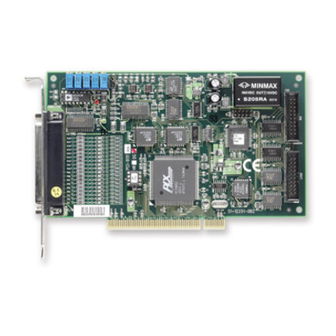
- Page 1 NuDAQ PCI-9111DG/HR Multi-Functions Data Acquisition Card User’s Guide...
- Page 2 Trademarks NuDAQ is registered trademarks of ADLINK Technology Inc. Other products names mentioned herein are used for identification purposes only and may be trademarks and/or registered trademarks of their respective...
- Page 3 Getting service from ADLINK Customer Satisfaction is always the most important thing for ADLINK Tech Inc. If you need any help or service, please contact us and get it. ADLINK Technology Inc. http://www.adlink.com.tw Web Site http://www.adlinktechnology.com Sales & Service service@adlink.com.tw NuDAQ nudaq@adlink.com.tw...
-
Page 5: Table Of Contents
Table of Contents Chatper 1 Introduction .......... 1 Features................1 Applications...............2 Specifications..............2 Software Supporting ............4 1.4.1 Programming Library............. 4 ® 1.4.2 PCIS-LVIEW: LabVIEW Driver..........5 1.4.3 PCIS-VEE: HP-VEE Driver............5 1.4.4 DAQBench : ActiveX Controls ........... 5 1.4.5 DASYLab PRO ..............6 1.4.6 PCIS-DDE: DDE Server and InTouch ...... - Page 6 Software Trigger Register..........19 3.10 Interrupt Control Register..........19 3.11 Hardware Interrupt Clear Register........20 3.12 A/D Mode & Interrupt Control Read Back Register..20 3.13 Extended I/O Ports ............21 3.14 Digital I/O register ............22 3.15 D/A Output Register ............22 3.16 Timer/Counter Register...........23 Chatper 4 Operation Theorem ......24 A/D Conversion ...............24 4.1.1 A/D Conversion Procedure ..........25...
- Page 7 5.10 _9111_EDO_Read_Back..........44 5.11 _9111_Set_EDO_Function ..........44 5.12 _9111_DA.................45 5.13 _9111_AD_Read_Data.............45 5.14 _9111_AD_Read_Data_Repeat ........46 5.15 _9111_AD_Set_Channel..........46 5.16 _9111_AD_Get_Channel ..........47 5.17 _9111_AD_Set_Range.............47 5.18 _9111_AD_Get_Range.............48 5.19 _9111_AD_Get_Status.............49 5.20 _9111_AD_Set_Mode ............50 5.21 _9111_AD_Get_Mode............50 5.22 _9111_INT_Set_Reg ............51 5.23 _9111_INT_Get_Reg ............52 5.24 _9111_Reset_FIFO............52 5.25 _9111_AD_Soft_Trigger ..........53 5.26 _9111_Set_8254...............53 5.27 _9111_Get_8254 ..............54 5.28 _9111_AD_Timer .............54 5.29 _9111_Counter_Start............55...
- Page 8 6.4.2 Bipolar Analog Output............69 Chatper 7 Software Utility ........70 9111util ................70 7.1.1 Running 9111util.exe............70 7.1.2 System Configuration ............71 7.1.3 Calibration................72 7.1.4 Functional Testing..............73 I_EEPROM ...............74 Product Warranty/Service ........75 Table of Contents...
- Page 9 How to Use This Guide This manual is designed to help you to use the PCI-9111. The manual describes the versatile functions and the operation theorem of the PCI-9111 card. It is divided into six chapters: Chapter 1, "Introduction", gives an overview of the product features, applications, and specifications.
-
Page 11: Chatper 1 Introduction
Introduction The PCI-9111 is an advanced data acquisition card based on the 32-bit PCI Bus architecture. High performance designs and the state-of-the-art technology make this card ideal for data logging and signal analysis applications in medical, process control, and etc. Features The PCI-9111 PCI Bus Advanced Data Acquisition Card provides the following advanced features:... -
Page 12: Applications
Pre-trigger Control Integral DC-to-DC converter for stable analog power source 37-pin D-type connector Compact size: half-size PCB Applications Industrial and laboratory ON/OFF control Energy management Communication 16 TTL/DTL compatible digital input channels Security controller Product test Period and pulse width measurement Event and frequency counting Waveform and pulse generation BCD interface driver... - Page 13 u Analog output (D/A) Number of Channel: 1 Resolution: 12-bit Output Range: jumper selectable Unipolar: 0~10V Bipolar: -10V~+10V Converter: DAC7541 or equivalent, monolithic multiplying Settling Time: 30 Linearity: 1/2 bit LSB Output driving capability: 5mA max. u Digital I/O (DIO) Numbers of Channel: 16 TTL compatible inputs and outputs Input Voltage: Low: Min.
-
Page 14: Software Supporting
ISaGRAF , and so on. All the software options are included in the ADLink CD. The non-free software drivers are protected with serial licensed code. Without the software serial number, you can still install them and run the demo version for two hours for demonstration purpose. -
Page 15: Pcis-Lview: Labview Driver
Windows 98, Windows NT and Windows 2000. The developing environment can be VB, VC++, Delphi, BC5, or any Windows programming language that allows calls to a DLL. The user’s guide and function reference manual of PCIS-DASK are in the CD. Please refer the PDF manual files under \\Manual_PDF\Software\PCIS-DASK PCIS-DASK/X: Include device drivers and shared library for Linux. -
Page 16: Dasylab Tm Pro
DDE stands for Dynamic Data Exchange specifications. The PCIS-DDE includes the PCI cards’ DDE server. The PCIS-DDE server is included in the ADLINK CD. It needs license. The DDE server can be used conjunction with any DDE client under Windows NT. -
Page 17: Chatper 2 Installation
What You Have In addition to this User's Manual, the package includes the following items: PCI-9111 Enhanced Multi-function Data Acquisition Card ADLINK CD Software Installation Guide If any of these items is missing or damaged, contact the dealer from whom you purchased the product. -
Page 18: Pci-9111'S Layout
Inspect the card module carton for obvious damage. Shipping and handling may cause damage to your module. Be sure there are no shipping and handing damages on the module before processing. After opening the card module carton, extract the system module and place it only on a grounded anti-static surface component side up. -
Page 19: Jumper Descriptions
Jumper Descriptions The only one jumper (JP1) on the PCI-9111 card is used to set the range of the analog output channel. The analog output range could be unipolar (0~10V) or bi-polar (-10V~+10V). The default setting is bi-polar. A n a l o g o u t p u t r a n g e i s -1 0 V ~ + 1 0 V J P 1 A n a l o g o u t p u t r a n g e i s... -
Page 20: Device Installation For Windows Systems
Installation Procedures 1. Turn off your computer. 2. Turn off all accessories (printer, modem, monitor, etc.) connected to your computer. 3. Remove the cover from your computer. 4. Setup jumpers on the PCI or CompactPCI card. 5. Select a 32-bit PCI slot. PCI slots are shorter than ISA or EISA slots, and are usually white or ivory. - Page 21 u CN 1: Digital Signal Input (DI 0 ~ 15) 20 19 +12V 18 17 DI 15 16 15 DI 14 DI 13 14 13 DI 12 DI 11 12 11 DI 10 DI 9 10 9 DI 8 DI 7 DI 6 DI 5 DI 4...
-
Page 22: Daughter Board Connection
u CN 3: Analog Input/Output, Extended I/O, Trigger Signals EDO3 EDO2 EDO1 EDO0 ExtTrg EDI3 D.GND EDI2 D.GND EDI1 +12V EDI0 PreTrg DA Out A.GND A.GND A.GND A.GND AI15 AI14 AI13 AI12 AI11 AI10 Figure 2.5 Pin Assignment of CN3 Legend: AI n : Analog Input Channel n (single-ended) -
Page 23: Connect With Acld-9137
2.8.2 Connect with ACLD-9137 The ACLD-9137 is a direct connector for all the cards which equipped with 37-pin D-sub connector. This board provides a simple way for connection. It is very suitable for the simple applications that do not need complex signal condition before the A/D conversion is performed. -
Page 24: Chatper 3 Registers Format
Registers Format The detailed descriptions of the regis ters format are specified in this chapter. This information is quite useful for the programmers who wish to handle the card by low-level programming. However, we suggest users have to understand more about the PCI interface then start any low-level programming. In addition, the contents of this chapter can help users understand how to use software driver to manipulate this card. -
Page 25: I/O Address Map
The PCI-9111 A/D data is stored in the FIFO after conversion. The data can be transferred to host memory by software only. The register format for 12 bits PCI-9111DG and 16 bits PCI-9111HR is bit-wise alignment but not fully compatible. For 12 bits PCI-9111 data, the 4 LSBs are used to memorize the channel number in which the AD data is stored. -
Page 26: A/D Channel Control Register
AD11 AD10 AD15 ~ AD0: Analog to digital data. AD11 is the Most Significant Bit (MSB) of PCI-9111DG while AD15 is the MSB of PCI-9111HR. AD0 is the Least Significant Bit (LSB). CH3 ~ CH0: A/D channel number from which the data is derived. -
Page 27: A/D Channel Read Back Register
A/D Channel Read Back Register The AD channel setting can be read back from this register. Address: BASE + 6h Attribute: read only Data Format: BASE+6h BASE+7h Where: CNn: channel number ASn: Auto scan channel number. There are 8 bits in this register. Under non-auto scan mode, the 4 LSBs (CN0~CN3) show the channel number setting and the 4 MSBs (AS3~AS0) is all ‘0’. -
Page 28: A/D Range And Status Read Back Register
A/D Range and Status Read back Register The A/D range setting and A/D FIFO status can be read back from this register. Address: BASE + 8h Attribute: read only Data Format: BASE+8h AD_BUSY FF_FF FF_HF FF_EF BASE+9h Where GC0~GC2: A/D Range control setting FF_EF: ‘0’... -
Page 29: Software Trigger Register
ASCAN: Auto Scan Control 0: Auto Scan OFF 1: Auto Scan ON Only the modes listed below can be applied on the PCI-9111 card: Bit 3 Bit 2 Bit 1 Bit 0 Mode Description PTRG EITS TPST ASCAN Software Trigger & Polling Timer Pacer Trigger External Trigger Note:... -
Page 30: Hardware Interrupt Clear Register
0: IRQ every Timer tick 1: IRQ when ExtTrg signal changes from ‘H’ to ‘L’ FFEN: FIFO enable pin 0: FIFO Enable (Power On Default value) 1: FIFO Disable (To reset FIFO, set FFEN sequence as 0 -> 1 -> 0) 3.11 Hardware Interrupt Clear Register Because of the PCI interrupt signal is level trigger, the interrupt clear register must be written to clear the flag after processing the interrupt... -
Page 31: Extended I/O Ports
3.13 Extended I/O Ports The PCI-9111 provides four extended input signals and four extended output signals. The signals are on the 37 pin connector. The extended output signals can be read back from the high nibble (4 MSBs) of the extended input port. -
Page 32: Digital I/O Register
3.14 Digital I/O register There are 16 digital input channels and 16 digital output channels are provided by the PCI-9111. The address Base + 1C is used to access digital inputs and control digital outputs. Address: BASE + 2h Attribute: read only Data Format: Base + 2h Base + 3h... -
Page 33: Timer/Counter Register
3.16 Timer/Counter Register Each 82C54 chip occupies 4 I/O address locations in the PCI-9111 as shown blow. Users can refer to 82C54 data sheet for the descriptions about all the features of 82C54. You can download the data sheet on the following web site: “http://support.intel.com/support/controllers/peripheral/231164.htm”... -
Page 34: Chatper 4 Operation Theorem
Operation Theorem The operation theorem of the functions on PCI-9111 card is described in this chapter. The functions include the A/D conversion, D/A conversion, Digital I/O and counter / timer. The operation theorem can help you to understand how to manipulate or to program the PCI-9111. -
Page 35: A/D Conversion Procedure
4.1.1 A/D Conversion Procedure For using the A/D converter, users must know about the property of the signal to be measured at first. The users can decide which channels to be used and connect the signals to the PCI-9111. Refer to section 2.7 ‘Connectors Pin Assignment’. - Page 36 Analog Input Signal Connection The PCI-9111 provides 16 single-ended analog input channels. The analog signal can be converted to digital value by the A/D converter. To avoid ground loops and get more accurate measurement of A/D value, it is q uite important to understand the signal source type.
-
Page 37: A/D Trigger Source Control
Signal Range The proper signal range is important for data acquisition. The input signal may be saturated if the A/D gain is too large. Sometimes, the resolution may be not enough if the signal is small. The maximum A/D signal range of PCI-9111 is +/- 10 volts when the A/D gain value is 1. -
Page 38: A/D Data Transfer Modes
interrupt to transfer data. It is also possible to use software FIFO polling to transfer data. The A/D trigger, A/D data transfer and Interrupt can be set independently, most of the complex applications can thus be covered. It's recommend to use this mode if your applications need a fixed and precise A/D sampling rate. - Page 39 FIFO every 10 ms without taking care how to trigger A/D or transfer A/D data. ADLINK recommend user to check your system to find out the user software‘s priority in the special application. If the application software is at the highest priority, to poll the FIFO every 10 ms is suitable.
-
Page 40: Pre-Trigger Control
FIFO Half-Full Interrupt Transfer Sometimes, the applications do not need real-time processing, but the foreground program is too busy to poll the FIFO data, then the FIFO half-full interrupt transfer mode is useful. In addition, as the external A/D trigger source is used, the sampling rate may not be easy to predict, then the method could be applied because the CPU only be interrupted when the FIFO is half-full, thus reserved the CPU load. -
Page 41: A/D Data Format
6. If A/D is stopped, set the Pre-Trigger Mode off and process the data which stored in the host memory. 7. Go to Step 1 to set the Pre-Trigger mode and wait the next pre-trigger event. The Pre-Trigger timing is shown as following: External Pre-Trigger A/D Data Set Pre-Trigger... - Page 42 The A/D converted data of 12 bits PCI-9111DG is on the 12 MSBs of the A/D data. The 4 LSB of the 16 bits A/D data are the channel number and must be truncated by software. The relationship between voltage and the A/D...
-
Page 43: Interrupt Control
Interrupt Control 4.2.1 System Architecture The PCI-9111‘s interrupt system is a powerful and flexible system which is suitable for A/D data acquisition and many applications. The system is a Dual Interrupt System. The dual interrupt means the hardware can generate two interrupt request signals in the same time and the software can service these two request signals by ISR. -
Page 44: Interrupt Source Control
PCI card and it will occupy the PC resource. It is not suggested to re-design the initial condition of the PCI card by users‘ own application software. If users want to disable the IRQ level, please use the ADLINK’s software utility to change the power on interrupt setting. -
Page 45: D/A Conversion
D/A Conversion The PCI-9111 has one analog output channel. The signal range can be uni-polar or bi-polar which are set by JP1. -10V Pin-30 (DA Out) Ref In D/A Converter To D/A Output Analog GND The operation of D/A conversion is simpler than A/D operation. You only need to write digital values into the D/A data registers and the corresponding voltage will be output from the DA Out (pin-30 of CN3). -
Page 46: Digital Input And Output
Digital Input and Output To program digital I/O operation is fairly straightforward. The digital input operation is just to read data from the corresponding registers, and the digital output operation is to write data to the corresponding registers. The digital I/O registers‘... -
Page 47: Pacer Trigger Source
4.6.2 Pacer Trigger Source The timer #1 and timer #2 are cascaded together to generate the timer pacer trigger of A/D conversion. The frequency of the pacer trigger is software controllable. The maximum pacer signal rate is 2MHz/4=500K which excess the maximum A/D conversion rate of the PCI-9111. -
Page 48: Chatper 5 C/C++ Library
This chapter describes the software library for operating this card. Only the functions in DOS library and Windows 95 DLL are described. Please refer to the PCIS-DASK function reference manual, which included in ADLINK CD, for the descriptions of the Windows 98/NT/2000 DLL functions. -
Page 49: Programming Guide
In DOS Environment: _{hardware_model}_{action_name}. e.g. _9111_Initial() . All functions in PCI-9111 driver are with 9111 as {hardware_model}. But they can be used by PCI-9111DG, PCI-9111HR. In order to recognize the difference between DOS library and Windows 95 library, a capital "... -
Page 50: 9111_Initial
_9111_Initial @ Description This function is used to initialize PCI_9111. Every PCI_9111 card has to be initialized by this function before calling other functions. @ Syntax C/C++ (DOS) U16 _9111_Initial (U16 *existCards, PCI_INFO *info) C/C++ (Windows 95) U16 W_9111_Initial (U16 *existCards, PCI_INFO *info) Visual Basic (Windows 95) W_9111_Initial (existCards As Integer, info As PCI_INFO) As Integer... -
Page 51: 9111_Do_Channel
_9111_DO_Channel @ Description This function is used to write data to digital output ports. There are 16 digital output channels on PCI_9111. You can control each digital output channel by this function directly. When performing this function, the digital output port is written and the output status will be changed to the value you had specified to do_data. -
Page 52: 9111_Di_Channel
@ Argument cardNo: The card number of PCI-9111 card initialized DIData: The value accessed from digital input port @ Return Code ERR_NoError _9111_DI_Channel @ Description This function is used to read data from digital input port. There are 16 digital input channels on PCI_9111. You can read each digital input channel by this function directly. -
Page 53: 9111_Edo
C/C++ (Windows 95) W_9111_EDI (U16 cardNo, U16 *DIData) Visual Basic (Windows 95) W_9111_EDI (ByVal cardNo As Integer, DIData As Integer) As Integer @ Argument cardNo: The card number of PCI-9111 card initialized DIData: The value accessed from extended digital input port @ Return Code ERR_NoError _9111_EDO... -
Page 54: 9111_Edo_Read_Back
5.10 _9111_EDO_Read_Back @ Description This function is used to read back the output data that is written to output port last time. @ Syntax C/C++ (DOS) _9111_EDO_Read_Back (U16 cardNo, U16 *DOData ) C/C++ (Windows 95) W_9111_EDO_Read_Back (U16 cardNo, U16 *DOData ) Visual Basic (Windows 95) W_9111_EDO_Read_Back (ByVal cardNo As Integer, DOData As Integer) As Integer... -
Page 55: 9111_Da
5.12 _9111_DA @ Description This function is used to write data to D/A converters. There are one Digital-to-Analog conversion channel on the PCI-9111. The resolution of each channel is 12 bit; i.e. the range is from 0 to 4095. @ Syntax C/C++ (DOS) _9111_DA (U16 cardNo, I16 DAData) C/C++ (Windows 95) -
Page 56: 9111_Ad_Read_Data_Repeat
5.14 _9111_AD_Read_Data_Repeat @ Description This function is used to read the AD conversion data n times continuously. @ Syntax C/C++ (DOS) U16 _9111_AD_Read_Data_Repeat (U16 cardNo, I16 far *ADData, U16 C/C++ (Windows 95) U16 W_9111_AD_Read_Data_Repeat (U16 cardNo, I16 *ADData, U16 Visual Basic (Windows 95) W_9111_AD_Read_Data_Repeat (ByVal cardNo As Integer, ADData As Integer, ByVal n As Integer) As Integer @ Argument... -
Page 57: 9111_Ad_Get_Channel
@ Argument cardNo: The card number of PCI-9111 card initialized. ADChannelNo: selected channel number or the ending channel number to perform A/D conversion. @ Return Code ERR_NoError 5.16 _9111_AD_Get_Channel @ Description This function reads from the multiplexer scan channel register to get the AD channel number and the value is stored in ADChannelNo. -
Page 58: 9111_Ad_Get_Range
Input Range (V) Gain Gain Code 10 V AD_B_10_V AD_B_5_V 2.5 V AD_B_2_5_V 1.25 V AD_B_1_25_V 0.625V X 16 AD_B_0_625_V @ Syntax C/C++ (DOS) U16 _9111_AD_Set_Range (U16 cardNo, U16 ADRange) C/C++ (Windows 95) U16 W_9111_AD_Set_Range (U16 cardNo, U16 ADRange) Visual Basic (Windows 95) W_9111_AD_Set_Range (ByVal cardNo As Integer, ByVal ADRange As Integer) As Integer @ Argument... -
Page 59: 9111_Ad_Get_Status
@ Syntax C/C++ (DOS) U16 _9111_AD_Get_Range (U16 cardNo, U16 *ADRange) C/C++ (Windows 95) U16 W_9111_AD_Get_Range (U16 cardNo, U16 *ADRange) Visual Basic (Windows 95) W_9111_AD_Get_Range (ByVal cardNo As Integer, ADRange As Integer) As Integer @ Argument cardNo: The card number of PCI-9111 card initialized ADRange: The programmable gain of A/D conversion, the possible values are:... -
Page 60: 9111_Ad_Set_Mode
5.20 _9111_AD_Set_Mode @ Description This function is used to set AD trigger and channel scan mode. Please refer to section 5.1.3 for the detailed description of AD trigger modes and section 5.1.5 for the description of Pre-Trigger mode control. @ Syntax C/C++ (DOS) U16 _9111_AD_Set_Mode (U16 cardNo, U16 ADMode) C/C++ (Windows 95) -
Page 61: 9111_Int_Set_Reg
Visual Basic (Windows 95) W_9111_AD_Get_Mode (ByVal cardNo As Integer, ADMode As Integer) As Integer @ Argument cardNo: The card number of PCI-9111 card initialized ADMode: The value of AD mode. The returned value could be one or a combination of the following modes: A_9111_AD_PreTrg_ON A_9111_AD_PreTrg_OFF A_9111_AD_External_SRC... -
Page 62: 9111_Int_Get_Reg
5.23 _9111_INT_Get_Reg @ Description This function i s used to get the AD mode setting and interrupt control setting by reading data from A/D mode and interrupt control read back register. The returned settings are stored in INTC. Please refer to section 4.7 and section 4.9 for the detailed definition of each bit of the returned data. -
Page 63: 9111_Ad_Soft_Trigger
5.25 _9111_AD_Soft_Trigger @ Description This function is used to trigger the A/D conversion by software. When the function is called, a trigger pulse will be generated and the converted data will be stored from address Base +0. @ Syntax C/C++ (DOS) U16 _9111_AD_Soft_Trigger (U16 cardNo) C/C++ (Windows 95) U16 W_9111_AD_Soft_Trigger (U16 cardNo) -
Page 64: 9111_Get_8254
5.27 _9111_Get_8254 @ Description This function is used to read PCI-9111 8254 Programmable Timer. The read value are stored in count. @ Syntax C/C++ (DOS) U16 _9111_Get_8254 (U16 cardNo, U16 ChannelNo, U8 *count) C/C++ (Windows 95) U16 W_9111_Get_8254 (U16 cardNo, U16 ChannelNo, U8 *count) Visual Basic (Windows 95) W_9111_Get_8254 (ByVal cardNo As Integer, ByVal ChannelNo As Integer, count As Byte) As Integer... -
Page 65: 9111_Counter_Start
@ Argument cardNo: The card number of PCI-9111 card initialized. frequency divider of timer #1 frequency divider of timer #2 @ Return Code ERR_NoError 5.29 _9111_Counter_Start @ Description The counter #0 of the PCI-9111 Timer/Counter chip can be freely programmed by the users. This function is used to program the counter #0. -
Page 66: 9111_Counter_Stop
U16 W_9111_Counter_Read (U16 cardNo, U16 *c0) Visual Basic (Windows 95) W_9111_Counter_Read (ByVal cardNo As Integer, c0 As Integer) As Integer @ Argument cardNo: The card number of PCI-9111 card initialized. c0: count value of counter#0 @ Return Code ERR_NoError 5.31 _9111_Counter_Stop @ Description This function is used to stop the timer operation. -
Page 67: 9111_Clr_Irq
@ Syntax C/C++ (DOS) void _9111_INT_Source_Control (U16 cardNo, U16 int1Ctrl, U16 int2Ctrl) C/C++ (Windows 95) void W_9111_INT_Source_Control (U16 cardNo, U16 int1Ctrl, U16 int2Ctrl) Visual Basic (Windows 95) W_9111_INT_Source_Control (ByVal cardNo As Integer, ByVal int1Ctrl As Integer, ByVal int2Ctrl As Integer) @ Argument cardNo: the card number of PCI-9111 card initialized. -
Page 68: 9111_Get_Irq_Channel
None 5.34 _9111_Get_IRQ_Channel @ Description This function is used to get the IRQ level of the PCI-9111 card used currently. @ Syntax C/C++ (DOS) void _9111_Get_IRQ_Channel (U16 cardNo, U16 *irq_no) C/C++ (Windows 95) void W_9111_Get_IRQ_Channel (U16 cardNo, U16 *irq_no) Visual Basic (Windows 95) W_9111_Get_IRQ_Channel (ByVal cardNo As Integer, irq_no As Integer) @ Argument... -
Page 69: 9111_Ad_Ffhf_Polling
5.36 _9111_AD_FFHF_Polling @ Description This function is used to perform powerful AD data transfer by applying half-full polling mode. This method checks the FIFO half full signal every time call this function. If the FIFO is not half-full, the software do not read data. -
Page 70: 9111_Ad_Hr_Aquire
@ Argument cardNo: the card number of PCI-9111 card initialized. ad_data: the 12bits A/D converted value. The data format can be referred to section 5.1.6 for details. @ Return Code ERR_NoError ERR_AD_AquireTimeOut 5.38 _9111_AD_HR_Aquire @ Description This function is used to trigger the A/D conversion data for PCI-9111HR by software trigger. - Page 71 After executing this function, it is necessary to check the status of the operation by using the function _9111_AD_INT_Status(). While all the specified count of data are acquired, the interrupt status will be changed to “AD_INT_STOP”.The function can perform on single A/D channel (autoscan is disable) or multiple A/D channels (autoscan is enable) with fixed analog input range.
-
Page 72: 9111_Ad_Ffhf_Int_Start
ad_buffer: the start address of the memory buffer t store the AD data, the buffer size must large than the number of AD conversion. the frequency devider of Timer#1. the frequency devider of Timer#2. @ Return Code ERR_InvalidADChannel ERR_AD_InvalidGain ERR_InvalidTimerValue ERR_NoError 5.40 _9111_AD_FFHF_INT_Start @ Description... -
Page 73: 9111_Ad_Int_Status
@ Argument cardNo: the card number of PCI-9111 card initialized. auto_scan: 0: autoscan is disabled. 1: autoscan is enabled. ad_ch_no: A/D channel number. If the auto_scan is set as enable, the selection sequence of A/D channel is: 0, 1, 2, 3, ... , [ad_ch_no], 0, 1, 2, 3, ... -
Page 74: 9111_Ad_Ffhf_Int_Status
@ Argument cardNo: the card number of PCI-9111 card initialized. status: the status of the INT data transfer, the valid status code are the following: AD_INT_RUN AD_INT_STOP count: the A/D conversion count number performed currently @ Return Code ERR_NoError 5.42 _9111_AD_FFHF_INT_Status @ Description This function is used to check the status of interrupt operation using AD FIFO Half Full Interrupt Transfer Mode. -
Page 75: 9111_Ad_Ffhf_Int_Restart
5.43 _9111_AD_FFHF_INT_Restart @ Description After calling _9111_AD_FFHF_INT_Start, the AD conversion and transfer won’t stop until the N blocks of conversion have been completed. After the N blocks of AD data are acquired, calling this function can restart the FIFO half full interrupt transfer without re-initial all the relative registers. However, if _9111_AD_INT_Stop has been called, the program should use _9111_AD_FFHF_INT_Start to restart interrupt transfer function. -
Page 76: 9111_Ad_Int_Stop
5.44 _9111_AD_INT_Stop @ Description This function is used to stop both the interrupt data transfer functions. After executing this function, the internal AD trigger is disabled and the AD timer is stopped. This function returns the number/block of data has been transferred, no matter whether the AD interrupt data transfer is stopped by this function. -
Page 77: Chatper 6 Calibration
Calibration In data acquisition process, how to calibrate the measurement devices to maintain its accuracy is very important. Users can calibrate the analog input and analog output channels under the users' operating environment for optimizing the accuracy. This chapter will guide you to calibrate your PCI-9111 to an accuracy condition. -
Page 78: Vr Assignment
VR Assignment There are five variable resistors (VR) on the PCI-9111 board to allow you making accurate adjustment on A/D and D/A channels. The function of each VR is specified as Table 6.1. D/A full scale adjustment D/A offset adjustment A/D offset adjustment A/D full scale adjustment A/D programmable amplifier offset adjustment... -
Page 79: D/A Adjustment
D/A Adjustment 6.4.1 Unipolar Analog Output 1. Set JP1 to select unipolar. Connect VDM (+) to CN3 pin-30 (DAOut) and VDM (-) to A.GND. 2. Write the digital value 0 to DAC. T rim VR2 to obtain 0V reading in the DVM 3. -
Page 80: Chatper 7 Software Utility
7.1.1 Running 9111util.exe After finishing the DOS installation, you can execute the utility by typing as follows: C> cd \ADLINK\DOS\9111\Util C> 9111UTIL The following diagram will be displayed on you screen. The message at the bottom of each window guides you how to select item, go to next step and change the default settings. -
Page 81: System Configuration
****** PCI-9111 Utility Rev. 1.0 ****** Copyright © 1995-1996, ADLINK Technology Inc. All rights reserved. <F1>: Configuration. <F2>: Calibration. <F3>: Function testing. <Esc>: Quit. >>> Select function key F1 ~ F3, or press <Esc> to quit. <<< 7.1.2 System Configuration This function guides you to configure the PCI-9111 card, and set the right hardware configuration. -
Page 82: Calibration
7.1.3 Calibration This function guides you to calibrate the PCI-9111. The calibration program serves as a useful test of the PCI-9111's A/D and D/A functions and can aid in troubleshooting if problems arise. Note: For an environment with frequently large changes of temperature vibration, months re-calibration... -
Page 83: Functional Testing
If you select 3, the following figure displays on the screen: If completed Step5 then press <Enter> to next step, <ESC> to abort. 7.1.4 Functional Testing This function is used to test the functions of PCI-9111, it includes Digital I/O testing, D/A testing, A/D polling testing, A/D Interrupt Testing, and A/D FIFO Half-Full Interrupt testing. -
Page 84: I_Eeprom
PCI-9111 board. After finishing the DOS installation, you can execute the utility by typing as follows: C> cd \ADLINK\DOS\9111\UTIL C> I_eeprom At first, this program prompts you to input the card type—9111. After specifying the card type, this program shows the instructions to guide you to enable or disable the interrupt of your PCI-9111 board. -
Page 85: Product Warranty/Service
Product Warranty/Service Seller warrants that equipment furnished will be free form defects in material and workmanship for a period of one year from the confirmed date of purchase of the original buyer and that upon written notice of any such defect, Seller will, at its option, repair or replace the defective item under the terms of this warranty, subject to the provisions and specific exclusions listed herein.
Need help?
Do you have a question about the NuDAQ PCI-9111DG and is the answer not in the manual?
Questions and answers