
Related Manuals for Motorola MVME167-32


Summary of Contents for Motorola MVME167-32
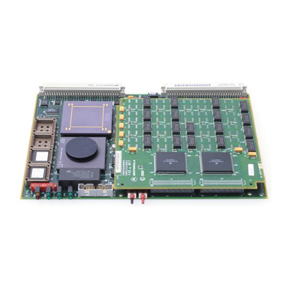
- Page 1 (217) 352-9330 | Click HERE Find the Emerson / Motorola MVME167-32 at our website:...
- Page 2 MVME167 Single Board Computer User’s Manual...
-
Page 4: Table Of Contents
Contents CHAPTER 1 GENERAL INFORMATION Introduction........................1-1 Model Designations ....................1-1 Features ........................1-2 Specifications ......................1-3 Cooling Requirements ..................1-3 FCC Compliance....................1-4 General Description ....................1-5 Equipment Required ....................1-6 Related Documentation....................1-7 Support Information....................1-8 Manual Terminology....................1-9 CHAPTER 2 HARDWARE PREPARATION AND INSTALLATION Introduction........................2-1 Unpacking Instructions ....................2-1 Hardware Preparation ....................2-1 General Purpose Readable Jumpers on Header J1..........2-2 System Controller Header J2 ................2-2... - Page 5 Normal Address Range ................3-3 Detailed I/O Memory Maps ................3-6 BBRAM,TOD Clock Memory Map .............3-26 Interrupt Acknowledge Map .................3-28 VMEbus Memory Map ..................3-29 VMEbus Accesses to the Local Bus .............3-29 VMEbus Short I/O Memory Map ..............3-29 Software Initialization ....................3-30 Multi-MPU Programming Considerations ............3-30 Local Reset Operation ..................3-30 CHAPTER 4 FUNCTIONAL DESCRIPTION...
- Page 6 APPENDIX A EIA-232-D INTERCONNECTIONS Introduction........................A-1 Levels of Implementation .................... A-3 Signal Adaptations....................A-3 Sample Configurations ..................A-4 Proper Grounding ....................A-6...
- Page 8 List of Figures Figure 2-1. MVME167 Switches, Headers, Connectors, Fuses, and LEDs ....2-3 Figure 4-1. MVME167 Main Module Block Diagram ..........4-11 Figure 4-2. Parity DRAM Mezzanine Module Block Diagram.......4-12 Figure 4-3. ECC DRAM Mezzanine Module Block Diagram ........4-13 Figure A-1. Middle-of-the-Road EIA-232-D Configuration ........A-4 Figure A-2.
- Page 10 List of Tables Table 1-1. MVME167 Model Designations...............1-1 Table 1-2. MVME167 Specifications ................1-4 Table 3-1. Local Bus Memory Map ................3-4 Table 3-2. Local I/O Devices Memory Map ..............3-5 Table 3-3. VMEchip2 Memory Map (Sheet 1 of 3)...........3-8 Table 3-4. PCCchip2 Memory Map .................3-14 Table 3-5.
-
Page 12: General Information
MVME167-004B (was MVME167-04 or -004A) 25 MHz 32MB Onboard Parity DRAM MVME167-031B (was MVME167-31 or -031A) 33 MHz 4MB Onboard ECC DRAM MVME167-032B (was MVME167-32 or -032A) 33 MHz 8MB Onboard ECC DRAM MVME167-033B (was MVME167-33 or -033A) 33 MHz 16MB Onboard ECC DRAM... -
Page 13: Features
General Information Features Features of the MVME167 are listed below. MC68040 Microprocessor at 25 MHz (-00X models), or 33 MHz (-03X models) 4/8/16/32/64MB of 32-bit DRAM with parity protection or 4/8/16/32/64/128/256MB of DRAM with ECC protection Four 44-pin PLCC ROM sockets (organized as two banks of 32 bits) 128KB SRAM (with optional battery backup) Status LEDs for FAIL, STAT, RUN, SCON, LAN, +12V (LAN power), SCSI, and VME. -
Page 14: Specifications
The following sections detail cooling requirements and FCC compliance. Cooling Requirements The Motorola MVME167 VMEmodule is specified, designed, and tested to operate reliably with an incoming air temperature range from 0° to 55° C (32° to 131° F) with forced air cooling at a velocity typically achievable by using a 100 CFM axial fan. -
Page 15: Fcc Compliance
General Information Table 1-2. MVME167 Specifications Characteristics Specifications Power requirements +5 Vdc (± 5%), 3.5 A (typical), 4.5 A (max.) (with all four EPROM (at 25 MHz, with 32MB parity DRAM); sockets populated and 5.0 A (typical), 6.5 A (max.) excluding external (at 33 MHz, with 128MB ECC DRAM) LAN transceiver) -
Page 16: General Description
General Description For minimum RF emissions, it is essential that the conditions above be implemented; failure to do so could compromise the FCC compliance of the equipment containing the module. General Description The MVME167 is a double-high VMEmodule based on the MC68040 microprocessor. The MVME167 has 4/8/16/32/64 MB of parity-protected DRAM or 4/8/16/32/64/128/256 MB of ECC-protected DRAM, 8KB of static RAM and time of day clock (with battery backup), Ethernet transceiver interface, four serial ports with... -
Page 17: Equipment Required
System Mode, which includes choices from a service menu. Refer to the MVME167Bug Debugging Package User’s Manual and the Debugging Package for Motorola 68K CISC CPUs User’s Manual for details. The MVME712X series of transition modules provide the interface between the MVME167 module and peripheral devices. -
Page 18: Related Documentation
The following publications are applicable to the MVME167 and may provide additional helpful information. If not shipped with this product, they may be purchased by contacting your local Motorola sales office. Non-Motorola documents may be purchased from the sources listed. -
Page 19: Support Information
Support Information The SIMVME167 manual contains the connector interconnect signal information, parts lists, and the schematics for the MVME167. This manual may be obtained free of charge by contacting your local Motorola sales office. MVME167 Single Board Computer User’s Manual... -
Page 20: Manual Terminology
Manual Terminology Manual Terminology Throughout this manual, a convention is used which precedes data and address parameters by a character identifying the numeric format as follows: dollar specifies a hexadecimal character percent specifies a binary number & ampersand specifies a decimal number Unless otherwise specified, all address references are in hexadecimal. - Page 21 General Information 1-10 MVME167 Single Board Computer User’s Manual...
-
Page 22: Hardware Preparation And Installation
HARDWARE PREPARATION AND INSTALLATION Introduction This chapter provides unpacking instructions, hardware preparation, and installation instructions for the MVME167. The MVME712X transition module hardware preparation is provided in separate manuals. Refer to Related Documentation in Chapter 1. Unpacking Instructions If the shipping carton is damaged upon receipt, request carrier’s agent be present during unpacking and inspection of equipment. -
Page 23: General Purpose Readable Jumpers On Header J1
Hardware Preparation and Installation System controller select (J2) Serial port 4 clock configuration select (J6 and J7) SRAM backup power source select (J8) (optional) General Purpose Readable Jumpers on Header J1 Each MVME167 may be configured with readable jumpers. These jumpers can be read as a register (at $FFF40088) in the VMEchip2 LCSR. -
Page 24: Figure 2-1. Mvme167 Switches, Headers, Connectors, Fuses, And Leds
Hardware Preparation MVME FAIL HALT RUN SCON +12V SCSI VME ABORT RESET Figure 2-1. MVME167 Switches, Headers, Connectors, Fuses, and LEDs MVME167/D3... -
Page 25: Serial Port 4 Clock Configuration Select Headers J6 And J7
Hardware Preparation and Installation Serial Port 4 Clock Configuration Select Headers J6 and J7 Serial port 4 can be configured to use clock signals provided by the RTXC4 and TRXC4 signal lines. Headers J6 and J7 on the MVME167 configure serial port 4 to drive or receive RTXC4 and TRXC4, respectively. -
Page 26: Sram Backup Power Source Select Header J8
Hardware Preparation SRAM Backup Power Source Select Header J8 Header J8 is an optional header that is used to select the power source used to back up the SRAM on the MVME167, if the optional battery and circuitry is present. Backup Power Disabled VMEbus +5V STBY Optional Battery... -
Page 27: Installation Instructions
Hardware Preparation and Installation Installation Instructions The following sections discuss installation of the MVME167 into a VME chassis, and system considerations. Ensure that EPROM devices are installed as needed. Factory configuration is with two EPROMs installed for the MVME167Bug debug monitor, in sockets XU1 and XU2. -
Page 28: System Considerations
MVME166/MVME167/MVME187 Single Board Computers Programmer’s Reference Guide.) Some cable(s) are not provided with the MVME712X module(s), and therefore are made or provided by the user. (Motorola recommends using shielded cables for all connections to peripherals to minimize radiation.) Connect the peripherals to the cable(s). Detailed information on the EIA-232-D signals supported is found in Appendix A. - Page 29 Hardware Preparation and Installation Multiple MVME167 modules may be configured into a single VME card cage. In general, hardware multiprocessor features are supported. Other MPUs on the VMEbus can interrupt, disable, communicate with and determine the operational status of the processor(s). One register of the GCSR set includes four bits which function as location monitors to allow one MVME167 processor to broadcast a signal to other MVME167 processors, if any.
-
Page 30: Operating Instructions
OPERATING INSTRUCTIONS Introduction This chapter provides necessary information to use the MVME167 module in a system configuration. This includes controls and indicators, memory maps, and software initialization of the module. Controls and Indicators The MVME167 module has ABORT and RESET switches; and FAIL, STAT, RUN, SCON, LAN,+12V (LAN power), SCSI, and VME indicators;... - Page 31 Operating Instructions The red FAIL LED (part of DS1) lights when the BRDFAIL signal line is active. The MC68040 status lines are decoded, on the MVME167, to drive the yellow STAT (status) LED (part of DS1). In this case, a halt condition from the processor lights the LED.
-
Page 32: Memory Maps
Memory Maps Memory Maps There are two points of view for memory maps: 1) the mapping of all resources as viewed by local bus masters (local bus memory map), and 2) the mapping of onboard resources as viewed by VMEbus Masters (VMEbus memory map). Local Bus Memory Map The local bus memory map is split into different address spaces by the transfer type (TT) signals. -
Page 33: Table 3-1. Local Bus Memory Map
Operating Instructions Table 3-1. Local Bus Memory Map Software Address Range Devices Accessed Port Size Size Cache Notes Inhibit $00000000 - DRAMSIZE User Programmable DRAMSIZE 1, 2 (Onboard DRAM) DRAMSIZE - $FF7FFFFF User Programmable D32/D16 3, 4 (VMEbus) $FF800000 - $FFBFFFFF $FFC00000 - $FFDFFFFF reserved $FFE00000 - $FFE1FFFF... -
Page 34: Table 3-2. Local I/O Devices Memory Map
Memory Maps The following table focuses on the Local I/O Devices portion of the local bus Main Memory Map.9. Table 3-2. Local I/O Devices Memory Map Address Range Devices Accessed Port Size Size Notes $FFF00000 - $FFF3FFFF reserved 256KB $FFF40000 - $FFF400FF VMEchip2 (LCSR) 256B $FFF40100 - $FFF401FF... -
Page 35: Detailed I/O Memory Maps
3-7 MCECC memory controller chip 3-13 TOD clock 3-8 CD2401 serial chip Note: Manufacturers’ errata sheets for the various chips are available by contacting your local Motorola sales representative. A non-disclosure agreement may be required. MVME167 Single Board Computer User’s Manual... - Page 36 Memory Maps This page intentionally left blank. MVME167/D3...
-
Page 37: Table 3-3. Vmechip2 Memory Map (Sheet 1 Of 3)
Operating Instructions Table 3-3. VMEchip2 Memory Map (Sheet 1 of 3) VMEchip2 LCSR Base Address = $FFF40000 OFFSET: SLAVE ENDING ADDRESS 1 SLAVE ENDING ADDRESS 2 SLAVE ADDRESS TRANSLATION ADDRESS 1 SLAVE ADDRESS TRANSLATION ADDRESS 2 ADDER PRGM DATA MASTER ENDING ADDRESS 1 MASTER ENDING ADDRESS 2 MASTER ENDING ADDRESS 3 MASTER ENDING ADDRESS 4... - Page 38 Memory Maps SLAVE STARTING ADDRESS 1 SLAVE STARTING ADDRESS 2 SLAVE ADDRESS TRANSLATION SELECT 1 SLAVE ADDRESS TRANSLATION SELECT 2 ADDER PRGM DATA MASTER STARTING ADDRESS 1 MASTER STARTING ADDRESS 2 MASTER STARTING ADDRESS 3 MASTER STARTING ADDRESS 4 MASTER ADDRESS TRANSLATION SELECT 4 MAST MAST MAST...
- Page 39 Operating Instructions Table 3-3. VMEchip2 Memory Map (Sheet 2 of 3) VMEchip2 LCSR Base Address = $FFF40000 OFFSET: BGTO GLOBAL TIME OFF TIME ON TIMER TICK TIMER 1 TICK TIMER 1 TICK TIMER 2 TICK TIMER 2 SCON PURS FAIL FAIL STAT PURS...
- Page 40 Memory Maps LOCAL PRESCALER ACCESS TIME OUT CLOCK ADJUST TIMER TIMER SELECT COMPARE REGISTER COUNTER COPARE REGISTER COUNTER OVERFLOW OVERFLOW COUNTER 2 COUNTER 1 SCALER SPARE IRQ7 IRQ6 IRQ5 IRQ4 IRQ3 IRQ2 IRQ1 P ERROR IRQ1E TIC TIMER 2 TIC TIMER 1 IRQ LEVEL IRQ LEVEL IRQ LEVEL...
- Page 41 Operating Instructions This page intentionally left blank. 3-12 MVME167 Single Board Computer User’s Manual...
- Page 42 Memory Maps Table 3-3. VMEchip2 Memory Map (Sheet 3 of 3) VMEchip2 GCSR Base Address = $FFF40100 Offsets VME- Local CHIP REVISION CHIP ID SIG3 SIG2 SIG1 SIG0 SCON SYSFL GENERAL PURPOSE CONTROL AND STATUS REGISTER 0 GENERAL PURPOSE CONTROL AND STATUS REGISTER 1 GENERAL PURPOSE CONTROL AND STATUS REGISTER 2 GENERAL PURPOSE CONTROL AND STATUS REGISTER 3 GENERAL PURPOSE CONTROL AND STATUS REGISTER 4...
-
Page 43: Table 3-4. Pccchip2 Memory Map
Operating Instructions Table 3-4. PCCchip2 Memory Map PCCchip2 Base Address = $FFF42000 OFFSET: CHIP ID CHIP REVISION TIC TIMER 1 TIC TIMER 1 TIC TIMER 2 TIC TIMER 2 PRESCALER COUNT REGISTER PRESCALER CLOCK ADJUST GPOE PLTY E/L* ICLR IRQ LEVEL SCC MODEM RTRY SCLR... - Page 44 Memory Maps MSTR FAST VECTOR BASE REGISTER BRAM COMPARE REGISTER COUNTER REGISTER COMPARE REGISTER COUNTER REGISTER OVERFLOW OVERFLOW COUNTER 2 COUNTER 1 TIC2 TIC2 TIC2 TIC TIMER 2 TIC1 TIC1 TIC1 TIC TIMER 1 ICLR IRQ LEVEL ICLR IRQ LEVEL SCC TRANSMIT SCC RECEIVE IRQ LEVEL...
-
Page 45: Table 3-5. Printer Memory Map
Operating Instructions Table 3-5. Printer Memory Map Printer ACK Interrupt Control Register $FFF42030 NAME PLTY E/L* ICLR Printer FAULT Interrupt Control Register $FFF42031 NAME PLTY E/L* ICLR Printer SEL Interrupt Control Register $FFF42032 NAME PLTY E/L* ICLR Printer PE Interrupt Control Register $FFF42033 NAME PLTY... -
Page 46: Table 3-6. Memc040 Internal Register Memory Map
Memory Maps Table 3-6. MEMC040 Internal Register Memory Map Data Bits MEMC040 MEMC040 $FFF43100 $FFF43000 CID7 CID6 CID5 CID4 CID3 CID2 CID1 CID0 $FFF43104 $FFF43004 REV7 REV6 REV5 REV4 REV3 REV2 REV1 REV0 $FFF43108 $FFF43008 FSTRD EXTPEN WPB* MSIZ2 MSIZ1 MSIZ0 $FFF4310C $FFF4300C... - Page 47 Operating Instructions Table 3-7. MCECC Internal Register Memory Map (Continued) MCECC Base Address = $FFF43000 (1st); $FFF43100 (2nd) Register Bit Names Register Register Offset Name DATA CONTROL DERC ZFILL RWCKB SCRUB CONTROL RACODE RADATA HITDIS SCRB SCRBEN SBEIEN IDIS SCRUB PERIOD SBPD15 SBPD14 SBPD13 SBPD12 SBPD11...
-
Page 48: Table 3-8. Cirrus Logic Cd2401 Serial Port Memory Map
Memory Maps Table 3-8. Cirrus Logic CD2401 Serial Port Memory Map Base Address = $FFF45000 Register Register Description Offsets Size Access Name Global Registers Global Firmware Revision Code Register GFRCR Channel Access Register Option Registers Channel Mode Register Channel Option Register 1 COR1 Channel Option Register 2 COR2... - Page 49 Operating Instructions Table 3-8. Cirrus Logic CD2401 Serial Port Memory Map (Continued) Base Address = $FFF45000 Register Register Description Offsets Size Access Name Channel Command and Status Registers Channel Command Register Special Transmit Command Register STCR Channel Status Register Modem Signal Value Registers MSVR-RTS MSVR-DTR Interrupt Registers...
- Page 50 Memory Maps Table 3-8. Cirrus Logic CD2401 Serial Port Memory Map (Continued) Base Address = $FFF45000 Register Register Description Offsets Size Access Name Modem Interrupt Registers Modem Priority Interrupt Level Register MPILR Modem Interrupt Register Modem (/Timer) Interrupt Status Register MISR Modem End Of Interrupt Register MEOIR...
- Page 51 Operating Instructions Table 3-8. Cirrus Logic CD2401 Serial Port Memory Map (Continued) Base Address = $FFF45000 Register Register Description Offsets Size Access Name Timer Registers Timer Period Register Receive Time-out Period Register RTPR R/W Async Receive Time-out Period Regis low RTPRl R/W Async Receive Time-out Period Register high...
-
Page 52: Table 3-9. 82596Ca Ethernet Lan Memory Map
Memory Maps Table 3-9. 82596CA Ethernet LAN Memory Map 82596CA Ethernet LAN Directly Accessible Registers Data Bits Address $FFF46000 Upper Command Word Lower Command Word $FFF46004 MPU Channel Attention (CA) NOTES: 1. Refer to the MPU Port and MPU Channel Attention registers in the MVME166/MVME167/MVME187 Single Board Computers Programmer’s Reference Guide. -
Page 53: Table 3-10. 53C710 Scsi Memory Map
Operating Instructions Table 3-10. 53C710 SCSI Memory Map 53C710 Register Address Map Base Address is $FFF47000 SCRIPTs Big Endian Mode and Mode Little Endian Mode SIEN SDID SCNTL1 SCNTL0 SOCL SODL SXFER SCID SBCL SBDL SIDL SFBR SSTAT2 SSTAT1 SSTAT0 DSTAT CTEST3 CTEST2... -
Page 54: Table 3-11. Mk48T08 Bbram,Tod Clock Memory Map
Memory Maps Table 3-11. MK48T08 BBRAM,TOD Clock Memory Map Address Range Description Size (Bytes) $FFFC0000 - $FFFC0FFF User Area 4096 $FFFC1000 - $FFFC10FF Networking Area $FFFC1100 - $FFFC16F7 Operating System Area 1528 $FFFC16F8 - $FFFC1EF7 Debugger Area 2048 $FFFC1EF8 - $FFFC1FF7 Configuration Area $FFFC1FF8 - $FFFC1FFF TOD Clock... -
Page 55: Bbram,Tod Clock Memory Map
(TOD) clock, is defined by the chip hardware. The first area is reserved for user data. The second area is used by Motorola networking software. The third area is used by the SYSTEM V/68 operating system. The fourth area is used by the MVME167 board debugger (MVME167Bug). - Page 56 Memory Maps char brd2_pwb[8]; char brd2_serial[8]; char reserved[153]; char cksum[1]; The fields are defined as follows: Four bytes are reserved for the revision or version of this structure. This revision is stored in ASCII format, with the first two bytes being the major version numbers and the last two bytes being the minor version numbers.
-
Page 57: Interrupt Acknowledge Map
15. The final one byte of the area is reserved for a checksum (as defined in the MVME167Bug Debugging Package User’s Manual and the Debugging Package for Motorola 68K CISC CPUs User’s Manual) for security and data integrity of the configuration area of the NVRAM. This data is stored in hexadecimal format. -
Page 58: Vmebus Short I/O Memory Map
Memory Maps VMEbus Short I/O Memory Map The VMEchip2 includes a user-programmable map decoder for the GCSR. The GCSR map decoder allows you to program the starting address of the GCSR in the VMEbus short I/O space. MVME167/D3 3-29... -
Page 59: Software Initialization
Operating Instructions Software Initialization Most functions that have been done with switches or jumpers on other modules are done by setting control registers on the MVME167. At powerup or reset, the EPROMs that contain the 167Bug debugging package set up the default values of many of these registers. -
Page 60: Functional Description
FUNCTIONAL DESCRIPTION Introduction This chapter provides a block diagram level description for the MVME167 module. The functional description provides an overview of the module, followed by a detailed description of several blocks of the module. The block diagram of the MVME167 is shown in Figure 4-1. -
Page 61: Mc68040 Mpu
Functional Description MC68040 MPU The MC68040 processor is used on the MVME167. The MC68040 has on-chip instruction and data caches and a floating point processor. Refer to the MC68040 user’s manual for more information. EPROM There are four 44-pin PLCC/CLCC EPROM sockets for 27C102JK or 27C202JK type EPROMs. -
Page 62: Onboard Dram
(ECC); two mezzanine boards may be stacked to provide 256MB of onboard RAM. The main board and a single mezzanine board together take one slot. The stacked configuration requires two VMEboard slots. Motorola software does support mixed parity and ECC memory boards on the same main board. The DRAM is four-way interleaved to efficiently support cache burst cycles. -
Page 63: Battery Backed Up Ram And Clock
Functional Description The DRAM map decoder can be programmed to accommodate different base address(es) and sizes of mezzanine boards. The onboard DRAM is disabled by a local bus reset and must be programmed before the DRAM can be accessed. Refer to the MEMC040 or the MCECC in the MVME166/MVME167/MVME187 Single Board Computers Programmer’s Reference Guide for detailed programming information. -
Page 64: Parallel Port Interface
MVME167 Functional Description or synchronous port. It can operate at synchronous bit rates up to 64 k bits per second. It uses RXD, CTS, DCD, TXD, RTS, and DTR. It also interfaces to the synchronous clock signal lines. Refer to the MVME166/MVME167/MVME187 Single Board Computers Programmer’s Reference Guide for drawings of the serial port interface connections. -
Page 65: Ethernet Interface
Functional Description The PCCchip2 provides an auto-strobe feature similar to that of the MVME147 PCC. In auto-strobe mode, after a write to the Printer Data Register, the PCCchip2 automatically asserts the STROBE* pin for a selected time specified by the Printer Fast Strobe control bit. -
Page 66: Scsi Termination
MVME167 Functional Description Support functions for the 53C710 are provided by the PCCchip2. Refer to the 53C710 user’s guide and to the MVME166/MVME167/MVME187 Single Board Computers Programmer’s Reference Guide for detailed programming information. SCSI Termination The system configurer must ensure that the SCSI bus is properly terminated at both ends. -
Page 67: Timing Performance
Functional Description bound cycles. VMEbus bound cycles are timed by the VMEbus access timer and the VMEbus global timer. Refer to the VMEchip2 in the MVME166/MVME167/MVME187 Single Board Computers Programmer’s Reference Guide for detailed programming information. Timing Performance This section provides the performance information for the MVME167. Various MVME167s are designed to operate at 25 MHz or 33 MHz. -
Page 68: Lan Dma Transfers
MVME167 Functional Description LAN DMA Transfers The MVME167 includes a LAN interface with DMA controller. The LAN DMA controller uses a FIFO buffer to interface the serial LAN bus to the 32-bit local bus. The FIFO buffer allows the LAN DMA controller to efficiently transfer data to the local bus. -
Page 69: Figure 4-1. Mvme167 Main Module Block Diagram
Functional Description P4, P5 J4, J5 SHEET 6 SHEET 8 SHEET 7 BBRAM AND TOD SHEET 23 SERIAL PORT MEZZANINE SERIAL SHEETS 24-26 PCCCHIP2 SHEET 21 MC68040 MPU PRINTER PORTS SHEET 27 PRINTER SHEET 22 SCSI INTERFACE SCSI SHEET 18 IPL COMBINER SHEET 28 LANCE... -
Page 70: Figure 4-2. Parity Dram Mezzanine Module Block Diagram
MVME167 Functional Description ADDRESS MUX MULTIPLEXED ADDRESS SHEET 7 MEMORY ARRAY RDA BUS BANK A SHEET 8 MEMORY ARRAY CONNECTOR ADDRESS BUS RDB BUS BANK B SHEET 5 SHEET 9 MEMORY ARRAY DATA MUX CONNECTORS DATA BUS RDC BUS BANK C SHEET 13, 14 SHEET 4 SHEET 10... -
Page 71: Figure 4-3. Ecc Dram Mezzanine Module Block Diagram
Functional Description Figure 4-3. ECC DRAM Mezzanine Module Block Diagram 4-12 MVME167 Single Board Computer User’s Manual... -
Page 72: Introduction
EIA-232-D INTERCONNECTIONS Introduction The EIA-232-D standard is the most widely used terminal/computer and terminal/modem interface, and yet it is not fully understood. This may be because not all the lines are clearly defined, and many users do not see the need to follow the standard in their applications. -
Page 73: Table A-1. Eia-232-D Interconnections
EIA-232-D Interconnections Table A-1. EIA-232-D Interconnections Pin Number Signal Mnemonic Signal Name and Description Not used. TRANSMIT DATA. Data to be transmitted; input to the modem from the terminal. RECEIVE DATA. Data which is demodulated from the receive line; output from the modem to the terminal. -
Page 74: Levels Of Implementation
Levels of Implementation 2. The EIA-232-D interface is intended to connect a terminal to a modem. When computers are connected without modems, one must be configured as a modem and the other as a terminal. Levels of Implementation There are several levels of conformance that may be appropriate for typical EIA-232- D interconnections. -
Page 75: Sample Configurations
EIA-232-D Interconnections Sample Configurations Figure A-1 is a good minimum configuration that almost always works. If the CTS and DCD signals are not received from the modem, the jumpers can be moved to artificially provide the needed signal. 6850 39kΩ -12V CONNECTOR +12V... -
Page 76: Figure A-2. Minimum Eia-232-D Connection
Levels of Implementation Figure A-2 shows a way of wiring an EIA-232-D connector to enable a computer to connect to a basic terminal with only three lines. This is feasible because most terminals have a DTR signal that is ON, and which can be used to pull up the CTS, DCD and DSR signals. -
Page 77: Proper Grounding
EIA-232-D Interconnections Proper Grounding Another subject to consider is the use of ground pins. There are two pins labeled GND. Pin 7 is the SIGNAL GROUND and must be connected to the distant device to complete the circuit. Pin 1 is the CHASSIS GROUND, but it must be used with care. The chassis is connected to the power ground through the green wire in the power cord and must be connected to the chassis to be in compliance with the electrical code. - Page 78 Index When using this index, keep in mind that a page number indicates only where referenced material begins. It may extend to the page or pages following the page referenced. Numerics big endian mode 3-24 binary number 1-9 167Bug (see debug monitor block diagram...
- Page 79 Index data bus structure 4-1 factory jumper settings 2-2 data circuit-terminating equipment FCC compliance 1-4 (DCE) A-1 features 1-2 data terminal equipment (DTE) A-1 forced air cooling 1-3 DCE (data circuit-terminating equip- front panel 3-1 ment) A-1 front panel indicators (DS1- DS4) 3-2 debug monitor (see...
- Page 80 interrupts 4-8 introduction 1-1, 2-1, 3-1, 4-1, A-1 manual terminology 1-9 map decoders 3-29 MC68040 MPU 4-2 J1 2-2 MCECC 1-5 J2 2-2 MCECC internal register memory map J3 4-10 3-17 J6 2-4 MEMC040 1-5 J7 2-4 MEMC040 internal register memory map J8 2-5 3-17 jumpers 2-1...
- Page 81 Index parity DRAM mezzanine module block multi-MPU programming consider- ations 3-30 diagram 4-12 MVME167 functional description 4-1 PCCchip2 1-5 MVME167 main module block diagram PCCchip2 memory map 3-14 4-11 printer interface 4-6 MVME167 model designations 1-1 printer memory map 3-16 MVME167 module installation 2-6 printer port 4-6 MVME167 specifications 1-4...
- Page 82 shielded cables (see also cables) 1-4, 2-7 TRXC4 (Transmit Receive Clock 4) 2-4 signal adaptations A-3 TT (transfer type) signals 3-3 signal ground A-6 signal levels A-1 unpacking instructions 2-1 signals transfer type (TT) 3-3 software initialization 3-30 VMEbus 3-29 software-programmable hardware inter- VMEbus accesses to the local bus 3-29 rupts 4-8...
- Page 83 Index IN-6 MVME167 Single Board Computer User’s Manual...
Need help?
Do you have a question about the MVME167-32 and is the answer not in the manual?
Questions and answers