
Related Manuals for Advantech PCE-5124


Summary of Contents for Advantech PCE-5124
-
Page 1: User Manual
PCE-5124 LGA775 Intel® Core™ 2 Quad / Core™ 2 Duo Processor-based 800/1066/1333 MHz FSB PICMG 1.3 Single Host Board with PCIe / DDR2 / Dual GbE LAN User Manual... - Page 2 Copyright This document is copyrighted, 2008, by Advantech Co., Ltd. All rights are reserved. Advantech Co., Ltd. reserves the right to make improve- ments to the products described in this manual at any time without notice. No part of this manual may be reproduced, copied, translated or transmit- ted in any form or by any means without the prior written permission of Advantech Co., Ltd.
- Page 3 A Message to the Customer Advantech Customer Services Each and every Advantech product is built to the most exacting specifica- tions to ensure reliable performance in the harsh and demanding condi- tions typical of industrial environments. Whether your new Advantech...
- Page 4 Do not attempt to recharge, force open, or heat the battery. Replace the battery only with the same or equivalent type recommended by the manufac- turer. Discard used batteries according to the manufacturer’s instructions. PCE-5124 User Manual...
- Page 5 Memory Compatibility Table 1.1: PCE-5124 Memory Tested for Compatibility Vendor Advantech Brand Size Speed Type ECC Memory 78.91G ELPIDA E5108AG-6E-E DDR2 N 2 667 92.420 (64x8) 78.01G ELPIDA E5108AGBG- DDR2 N 2 667 92.420 6E-E (64x8) TS64M 96D2- SEC K4T51083QC...
- Page 6 Advantech assumes no liability under the terms of this warranty as a consequence of such events. If an Advantech product is defective, it will be repaired or replaced at no charge during the warranty period. For out-of-warranty repairs, you will be billed according to the cost of replacement materials, service time and freight.
- Page 7 5124 mechanically and electrically before shipment. It should be free of marks and scratches and in perfect working order upon receipt. As you unpack the PCE-5124, check it for signs of shipping damage. (For exam- ple, damaged box, scratches, dents, etc.) If it is damaged or it fails to meet the specifications, notify our service department or your local sales repre- sentative immediately.
- Page 8 PCE-5124 User Manual viii...
-
Page 9: Table Of Contents
Table 1.2:Connector list..........7 Board Layout: Jumper and Connector Locations....9 Figure 1.1:Jumper and connector locations ....9 PCE-5124 Block Diagram..........10 Figure 1.2:PCE-5124 block diagram ......10 Safety Precautions ............11 Jumper Settings ............... 12 1.8.1 How to set jumpers ............12 1.8.2... - Page 10 Figure 3.9:APM configuration........52 Figure 3.10:Configure remote access type and parameters ..............53 PCI/PNP Setup ..............54 Figure 3.11:PCI/PNP setup........... 54 3.4.1 Clear NVRAM.............. 54 3.4.2 Plug and play O/S ............54 3.4.3 PCI latency timer ............55 PCE-5124 User Manual...
- Page 11 3.4.4 Allocate IRQ to PCI VGA ..........55 3.4.5 Palette snooping............55 3.4.6 PCI IDE BusMaster ............55 3.4.7 Off board PCI/ISA IDE card ........55 3.4.8 IRQ................55 Boot Setup Utility............56 Figure 3.12:Boot setup utility ........56 Figure 3.13:Boot setting configuration......57 Security Setup ..............
- Page 12 Table B.14:Reset connector (JFP1 / RESET)..... 112 B.15 HDD LED (JFP2 / HDDLED) ........112 Table B.15:HDD LED (JFP2 / HDDLED)....112 B.16 ATX Soft Power Switch (JFP1 / PWR_SW) ....113 Table B.16:ATX soft power switch (JFP1 / PWR_SW)........113 PCE-5124 User Manual...
- Page 13 B.17 Hi-definition Audio Link Connector (HDAUD1) ..113 Table B.17:Hi-definition audio link connector (HDAUD1)..........113 B.18 SM Bus Connector (JFP2 / SNMP)....... 114 Table B.18:SM bus connector (JFP2 / SNMP)... 114 B.19 LAN1 and LAN2 LED Connector (LANLED1)... 114 Table B.19:LAN1 and LAN2 LED connector (LANLED1) ..........
- Page 14 PCE-5124 User Manual...
- Page 15 Hardware Configura- tion Chapter 1...
-
Page 16: Chapter 1 Hardware Configuration
PCE-5124 also has rich I/O interfaces, it's 6 SATA2 ports can support software RAID 0, 1, 10, 5 to be a cost-effective data reliability solution, the 6 on-board serial ports (COM ports) allows PCE-5124 to meet various industrial control applications. -
Page 17: Features & Benifits
1.2 Features & Benifits Features Benefits Support Intel’s most advanced 45-nm and Supporting Intel® Core 2 Quad 65-nm manufacture technology, multi-core / Core 2 Duo / Pentium® Dual- processors that are with high performance core/ Celeron® 400 Series pro- and low power consumption ( 65W), suit- cessors able for applications that need strong computing power and high reliability. -
Page 18: Specifications
300 MB/s. These interfaces can be enabled/disabled in the BIOS. Note: PCE-5124 does NOT support PATA(IDE) inter- face. • Floppy disk drive interface: Supports one floppy disk drive, 5¼" (360 KB and 1.2 MB) or 3½" (720 KB, 1.44 MB). These interfaces can be enabled/disabled in the BIOS. -
Page 19: Input/Output
1.3.3 Input/Output • PCI express lanes: One PCI-E x 16 and four PCI-E x 1 lanes to the backplane. • PCI bus: Four PCI masters to the backplane, 32-bit, 33 MHz PCI 2.2 compliant. • Enhanced parallel port: This EPP/SPP/ECP port can be configured to LPT1, LPT2, LPT3 or disabled. -
Page 20: Mechanical And Environmental Specifications
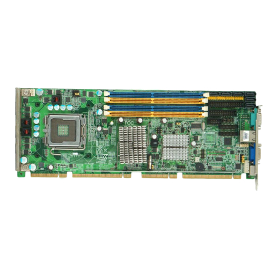
• Board weight: 0.490 kg 1.4 Jumpers and Connectors Connectors on the PCE-5124 single host board link it to external devices such as hard disk drives and a keyboard. In addition, the board has a num- ber of jumpers used to configure your system for your application. -
Page 21: Table 1.2:Connector List
Table 1.2: Connector list Label Function FDD1 FDD connector Parallel port, Parallel port x 1, supports SPP/EPP/ LPT1 ECP mode LAN1 GbE LAN1 / Intel 82566DM LAN2 GbE LAN2 / Intel 82573V VGA1 VGA connector KBMS1 PS/2 keyboard and mouse connector KBMS2 External keyboard/mouse connector COM1... - Page 22 SATA5 Serial ATA5 SATA6 Serial ATA7 Buzzer CPU1 CPU Socket DIMMA1 Memory connector channel A DIMMA2 Memory connector channel A DIMMB1 Memory connector channel B DIMMB2 Memory connector channel B GPIO1 GPIO pin header (SMD pitch-2.0 mm) PCE-5124 User Manual...
-
Page 23: Board Layout: Jumper And Connector Locations
1.5 Board Layout: Jumper and Connector Locations CPUFAN1 CPUSOCKET JFP1 JFP2 JFP3 DIMMA1 DIMMA2 DIMMB1 DIMMB2 CMOS1 HDAUD1 JCASE1 GPIO1 SATA1 USB12 JWDT1 J1R1 JOBS1 KBMS2 USB78 VGA1 KBMS1 COM1 LAN1 LAN2 LANLED1 SATA6 JSETCOM2 Figure 1.1: Jumper and connector locations Chapter 1... -
Page 24: Pce-5124 Block Diagram
Intel 82573 Codec PCI-Express*1 ICH9 DO PCI-Express*1 USB 2.0/1.1 8 USB Connector A PCI-Express*1 Ports PCI-Express*1 4 USB Ports Connector D 32 bit/33 MHz Connector C PCI Bus Super IO BIOS Winbond W83627HG Figure 1.2: PCE-5124 block diagram PCE-5124 User Manual... -
Page 25: Safety Precautions
1.7 Safety Precautions Warning! Always completely disconnect the power cord from your chassis whenever you work with the hardware. Do not make connections while the power is on. Sensitive electronic components can be damaged by sudden power surges. Only experienced electronics personnel should open the PC chassis. -
Page 26: Jumper Settings
1.8.2 CMOS clear (CMOS1) The PCE-5124 CPU card contains a jumper that can erase CMOS data and reset the system BIOS information. Normally this jumper should be set with pins 1-2 closed. If you want to reset the CMOS data, set J1 to 2-3 closed for just a few seconds, and then move the jumper back to 1-2 closed. - Page 27 CMOS1 Chapter 1...
-
Page 28: Watchdog Timer Output (Jwdt1)
1.8.3 Watchdog timer output (JWDT1) The PCE-5124 contains a watchdog timer that will reset the CPU or send a signal to IRQ11 in the event the CPU stops processing. This feature means the PCE-5124 will recover from a software failure or an EMI problem. - Page 29 JIR1 JOBS1 JWDT1 Chapter 1...
-
Page 30: Com2 Rs-232/422/485 Mode Selector (Jestcom2)
Table 1.6: COM2 RS-232/422/485 mode selector Function Jumper Setting RS-232 (5-6) + (7-9) + (8-10) + (13-15) + (14-16) closed RS-422 (3-4) + (9-11) + (10-12) + (15-17) + (16-18) closed RS-485 (1-2) + (9-11) + (10-12) + (15-17) + (16-18) closed PCE-5124 User Manual... - Page 31 COM1 COM5-6 COM3-4 JSETCOM2 COM2 Chapter 1...
-
Page 32: System Memory
1.9 System Memory The PCE-5124 has four sockets for 240-pin dual inline memory modules (DIMMs) in two memory channels. All these sockets use 1.8 V unbuffered double data rate synchronous DRAMs (DDR SDRAM). They are available in capacities of 256 MB, 512 MB, 1024 MB and 2 GB. -
Page 33: Memory Installation Procedures
0 DIMM slots (DIMMA1 and DIMMA2) empty, or it may cause some system abnormal- ity. 1.11 Cache Memory Those CPUs supported by PCE-5124 have 12 MB, 8MB, 6 MB, 4MB, 3MB, 2MB, 1 MB, 512KB L2 cache memory sizes. 1.12 Processor Installation Warning! - Page 34 Step 1. Pull the bar beside the CPU socket outward and lift it. Step 2. Align the triangular marking on the processor with the cut edge of the socket. Step 3. Put the back socket cap and press down the bar to fix it. PCE-5124 User Manual...
- Page 35 Connecting Peripherals Chapter 2...
-
Page 36: Chapter 2 Connecting Peripherals
You can access most of the connectors from the top of the board as it is being installed in the chassis. If you have a number of cards installed, you may need to partially remove the card to make all the connections. PCE-5124 User Manual... -
Page 37: Floppy Drive Connector (Fdd1)
2.2 Floppy Drive Connector (FDD1) LPT1 FDD1 You can attach up to two floppy disk drives to the PCE-5124's onboard controller. You can use 3.5" (720 KB, 1.44 MB) drives. The motherboard comes with a 34-pin daisy-chain drive connector cable. -
Page 38: Parallel Port (Lpt1)
2.3 Parallel Port (LPT1) LPT1 FDD1 The parallel port is normally used to connect the motherboard to a printer. The PCE-5124 includes an onboard parallel port, accessed through a 26- pin flat-cable connector, LPT1. PCE-5124 User Manual... -
Page 39: Usb Ports (Usb12, Usb34, Usb56, Usb78)
2.4 USB Ports (USB12, USB34, USB56, USB78) The PCE-5124 provides up to eight USB (Universal Serial Bus) ports with complete Plug & Play and hot swap support for up to 127 external devices. These USB ports comply with USB Specification Rev. 2.0, sup- port transmission rates up to 480 Mbps and are fuse protected. -
Page 40: Vga Connector (Vga1)
2.5 VGA Connector (VGA1) VGA1 The PCE-5124 includes a VGA interface that can drive conventional CRT displays. VGA1 is a standard 15-pin D-SUB connector commonly used for VGA. Pin assignments for VGA1 are detailed in Appendix B. PCE-5124 User Manual... -
Page 41: Serial Ports (Com1, Com2, Com3-4 & Com5-6)
2.6 Serial Ports (COM1, COM2, COM3-4 & COM5-6) COM5-6 COM1 COM3-4 JESTCOM2 COM2 Chapter 2... - Page 42 The PCE-5124 offers six serial ports. The user can use JSETCOM2 to select among RS-232/422/485 modes for COM2. These ports can connect to serial devices, such as a mouse or a printer, or to a communications network. The IRQ and address ranges for both ports are fixed. However, if you want to disable the port or change these parameters later, you can do this in the system BIOS setup.
-
Page 43: Ps/2 Keyboard And Mouse Connector (Kbms1)
2.7 PS/2 Keyboard and Mouse Connector (KBMS1) KBMS2 KBMS1 Two on-board 6-pin mini-DIN connectors (KBMS1) provide connection to PS/2 keyboard and mouse by the Y-cable (1700060202) in the package. The on-board KBMS2 pin header provide connection the the front panel PS/2 keybaord and mouse connector of the chassis. -
Page 44: Cpu Fan Connector (Cpufan1)
2.8 CPU Fan Connector (CPUFAN1) This connector supports cooling fans of 500 mA (6 W) or less. CPUFAN1 PCE-5124 User Manual... -
Page 45: Front Panel Connectors (Jfp1, Jfp2 & Jfp3)
2.9 Front Panel Connectors (JFP1, JFP2 & JFP3) There are several external switches to monitor and control the PCE-5124. JFP1~3 2.9.1 Power LED and keyboard lock (JFP3) JFP3 is a 5-pin connector for the power LED. Refer to Appendix B for detailed information on the pin assignments. -
Page 46: Table 2.1:Ps/2 Or Atx Power Supply Led Status
System Off Slow flashes 2.9.2 External speaker (JFP2) JFP2 is a 4-pin connector for an external speaker. The PCE-5124 provides an onboard buzzer as an alternative to an external speaker. To enable the buzzer, set pins 5 and 7 as closed. -
Page 47: H/W Monitor Alarm (Jobs1)
2.10 H/W Monitor Alarm (JOBS1) JIR1 JOBS1 JWDT1 Close: Enable OBS Alarm Open: Disable OBS Alarm Chapter 2... -
Page 48: Lan Ports (Lan1 & Lan2)
2.11 LAN Ports (LAN1 & LAN2) LAN1 LAN2 The PCE-5124 is equipped with one or two high-performance 1000 Mbps Ethernet LANs. They are supported by all major network operating sys- tems. The RJ-45 jacks on the rear plate provide convenient connectivity. -
Page 49: High Definition Audio Module Interface
2.12 High Definition Audio Module Interface HDAUD1 This HDAUD1 pin header is the connection interface to Advantech's 7.1 channel high definition audio module. Note: Advantech 7.1 channel high definition audio module ordering information. P/N: PCA-AUDIO-HDA1E Chapter 2... -
Page 50: Gpio Header (Gpio1)
2.13 GPIO Header (GPIO1) GPIO1 Provides 14-Pins pin header for Digital I/O usage. Refer to Appendix B for detailed information on the pin assignments and programming guide in Appendix C. PCE-5124 User Manual... -
Page 51: Case Open Connector (Jcase1)
2.14 Case Open Connector (JCASE1) JCASE1 The 2-pin case open connector is for chassis with a case open sensor. While opening the case, the buzzer on motherboard will beep. Chapter 2... -
Page 52: Front Panel Lan Indicator Connector (Lanled1)
2.15 Front Panel LAN Indicator Connector (LANLED1) Table 2.3: Front Panel LAN Indicator Connector LAN Mode Indicator G-LAN Link ON Green ON G-LAN Active Green Flash G-LAN Link Off Green OFF LANLED1 PCE-5124 User Manual... -
Page 53: Serial Ata Interface (Sata1~Sata6)
2.16 Serial ATA Interface (SATA1~SATA6) SATA1 SATA6 The PCE-5124 features high performance serial ATA interfaces (up to 300 MB/s) those eases cabling to hard drives or CD/DVD drives with thin and long cables. These six on-board SATA ports can be configured as RAID 0, 1, 10, 5. - Page 55 AMI BIOS Setup Chapter 3...
-
Page 56: Figure 3.1:Setup Program Initial Screen
The Setup program uses a number of menus for making changes and turning the special features on or off. This chapter describes the basic navigation of the PCE-5124 setup screens. Figure 3.1: Setup program initial screen AMI’s BIOS ROM has a built-in Setup program that allows users to mod-... -
Page 57: Entering Setup
3.1 Entering Setup Turn on the computer and check for the “patch” code. If there is a number assigned to the patch code, it means that the BIOS supports your CPU. If there is no number assigned to the patch code, please contact an Advan- tech application engineer to obtain an up-to-date patch code file. -
Page 58: Main Setup
Time or System Date using the <Arrow> keys. Enter new values through the keyboard. Press the <Tab> key or the <Arrow> keys to move between fields. The date must be entered in MM/DD/YY format. The time must be entered in HH:MM:SS format. PCE-5124 User Manual... -
Page 59: Advanced Bios Features Setup
3.3 Advanced BIOS Features Setup Select the Advanced tab from the PCE-5124 setup screen to enter the Advanced BIOS Setup screen. You can select any of the items in the left frame of the screen, such as CPU Configuration, to go to the sub menu for that item. -
Page 60: Cpu Configuration
When enabled through the BIOS, two 64-byte cache lines are fetched into a 128-byte sector, regardless of whether the additional cache line has been requested or not. You may choose to enable or disable it. PCE-5124 User Manual... - Page 61 Max CPUID Value Limit This is disabled for Windows XP. Intel(R) Virtualization Technology This feature is used to enable or disable the Intel Virtualization Technol- ogy (IVT) extension. It allows multiple operating systems to run simulta- neously on the same system. It does this by creating virtual machines, each running its own x86 operating system.
-
Page 62: Ide Configuration
AHCI is a new interface specification that allows the SATA controller driver to support advanced features. While entering setup, BIOS auto detects the presence of AHCI devices. This displays the status of auto detection of AHCI devices. PCE-5124 User Manual... -
Page 63: Super I/O Configuration
3.3.3 Super I/O configuration Figure 3.7: Super I/O configuration Chapter 3... - Page 64 This option configures serial port 3/4 base addresses. Serial Port 3/4/5/6 IRQ This option configures serial port 3/4 base IRQ. Parallel Port Address This configures parallel port base addresses. The following options are also available: • Parallel Port Mode • Parallel Port IRQ PCE-5124 User Manual...
-
Page 65: Hardware Health Function
3.3.4 Hardware health function Figure 3.8: Hardware health configuration. Hardware health function Enable/Disable the onboard hardware monitor controller. If this option is enabled, the BIOS and OBS utility can get the system board’s health information from hardware monitor controller. Chassis Intrusion Enable/Disable the Chassis Intrusion monitoring function. -
Page 66: Apm Configuration
Enter Suspend after the specified time. Throttle Slow Clock Ratio Select the duty cycle in throttle mode. Keyboard & PS/2 Mouse When you set this to Monitor, you can monitor the PS/2 keyboard and mouse ports. Power Button Mode PCE-5124 User Manual... - Page 67 Power on, off or enter suspend mode when the power button is pressed. The following options are also available. • Resume On Ring: Disable/Enable RI wake event. • Resume On LAN: Disable/Enable LAN PME wake event. • Resume On RTC Alarm: Disable/Enable RTC wake event. Figure 3.10: Configure remote access type and parameters Remote Access You can disable or enable the BIOS remote access feature here.
-
Page 68: Pci/Pnp Setup
3.4 PCI/PNP Setup Select the PCI/PnP tab from the PCE-5124 setup screen to enter the Plug and Play BIOS Setup screen. You can display a Plug and Play BIOS Setup option by highlighting it using the <Arrow> keys. All Plug and Play BIOS Setup options are described in this section. -
Page 69: Pci Latency Timer
3.4.3 PCI latency timer Use this to adjust the PCI Latency Timer. This option sets the latency of all PCI devices on the PCI bus. The Optimal and Fail-Safe default setting is 64. 3.4.4 Allocate IRQ to PCI VGA Set this value to allow or stop the system from giving the VGA adapter card an interrupt address. -
Page 70: Boot Setup Utility
3.5 Boot Setup Utility Figure 3.12: Boot setup utility PCE-5124 User Manual... -
Page 71: Figure 3.13:Boot Setting Configuration
Figure 3.13: Boot setting configuration The following options are available: • Quick Boot: Allows the BIOS to skip certain tests while booting. This will decrease the time needed to boot the system. • Quiet Boot: If this option is set to Disabled, the BIOS displays normal POST messages. -
Page 72: Security Setup
To access the sub menu for the follow- ing items, select the item and press <Enter>: • Change Supervisor Password • Boot sector Virus protection: The boot sector virus protection will warn if any program tries to write to the boot sector. PCE-5124 User Manual... -
Page 73: Advanced Chipset Settings
3.7 Advanced Chipset Settings Figure 3.15: Advanced Chipset Settings Chapter 3... -
Page 74: Figure 3.16:North Bridge Configuration
• Boots Graphic Adapter Priority: Select which graphics controller to use as the primary boot device. • Internal Graphics Mode Select: Select the amount of system memory used by the Internal graphics device. • PEG Port: Auto or Disabled. • PEG Force x1: Enabled or Disabled. PCE-5124 User Manual... -
Page 75: Figure 3.17:Video Function Configuration
Figure 3.17: Video function configuration DVMT model select Displays the active system memory mode. DVMT / FIXED Memory Specify the amount of DVMT / FIXED system memory to allocate for video memory. Spread spectrum clock Enable/Disable spread spectrum. Chapter 3... -
Page 76: Figure 3.18:South Bridge Configuration
• GbE LAN boot: Enables or disables GbE LAN boot. • LAN2 Controller: Enables or disables the LAN2 controller. • HDA Controller: Enables or disables the HDA controller. • SMBUS Controller: Enables or disables the SMBUS controller. PCE-5124 User Manual... -
Page 77: Exit Option
3.8 Exit Option Figure 3.19: Exit option 3.8.1 Save changes and exit When you have completed system configuration, select this option to save your changes, exit BIOS setup and reboot the computer so the new system configuration parameters can take effect. Select Exit Saving Changes from the Exit menu and press <Enter>. -
Page 78: Discard Changes And Exit
Select Fail- Safe Defaults if your computer is experiencing system configuration problems. Select Load Fail-Safe Defaults from the Exit menu and press <Enter>. The following message appears: Load Fail-Safe Defaults? [OK] [Cancel] Select OK to load Fail-Safe defaults. PCE-5124 User Manual... - Page 79 Chipset Software Installation Utility Chapter 4...
-
Page 80: Chapter 4 Chipset Software Install Utility
To facilitate the installation of the enhanced display drivers and utility software, read the instructions in this chapter carefully. The drivers for the PCE-5124 are located on the software installation CD. The Intel Chipset Software Installation Utility is not required on any systems run- ning Windows NT 4.0. -
Page 81: Windows Xp Driver Setup
• Identification of Intel (R) Chipset Components in the Device Manager Note: This utility is used for the following versions of Windows, and it has to be installed before installing all the other drivers: • Microsoft Windows Vista • Microsoft Windows Vista x64 Edition* •... - Page 82 Click “Yes” when you see the following message. PCA-6194 User Manual...
- Page 83 Click “Next” when you see the following message. Chapter 4...
- Page 84 When the following message appears, click “Finish” to complete the installation and restart Windows.
- Page 85 VGA Setup Chapter 5...
-
Page 86: Chapter 5 Vga Setup
Chapter 4 for information on installing the CSI utility. Insert the driver CD into your system’s CD-ROM drive. Select the folder “VGA” then click the proper VGA driver for the OS. Windows XP is used as an example in the following steps. PCE-5124 User Manual... - Page 87 Click “Next” to continue the installation. You will see a welcome window. Please click “Yes” to continue the installation. . Chapter 5...
- Page 88 Click “Finish” to complete the installation and restart the computer now or later. PCE-5124 User Manual...
- Page 89 Chapter 5...
- Page 91 Onboard Security Setup Chapter 6...
-
Page 92: Chapter 6 Onboard Security Setup
Chapter 6 Onboard Security Setup 6.1 Introduction The PCE-5124's hardware monitor is based on the Winbond W83627HG chip. Onboard security (OBS) functions monitor key hardware to help you maintain system stability and durability. The PCE-5124 can monitor five sets of positive system voltages, two sets of system negative volt- ages, CPU cooling fan speed, and CPU temperature. - Page 93 Click “Next” when you see the following message. Click “Next” when you see the following message.. Chapter 6...
-
Page 94: Using The Obs Hardware Doctor Utility
From Windows desktop, click on “Start” and select “Programs”, select “Win bond HWDoctor” and click “HWDOCTOR”. It is recommended that you load the default values for all the OBS settings. However, if desired, you can establish new conditions for voltage, fan speed and tem- perature. PCE-5124 User Manual... - Page 95 Chapter 6...
- Page 96 PCE-5124 User Manual...
- Page 97 LAN Configuration Chapter 7...
-
Page 98: Chapter 7 Lan Configuration
Chapter 7 LAN Configuration 7.1 Introduction The PCE-5124 has a single/dual Gigabit Ethernet LAN interface (Intel 82566DM and 82573V) that is connected to a dedicated PCIe x1 link to eliminating network bottlenecks by offering a bandwidth of up to 500 MB/s. -
Page 99: Win Xp Driver Setup (Lan)
7.4 Win XP Driver Setup (LAN) Insert the driver CD into your system’s CD-ROM drive. Selecting the folder “LAN” then click the proper LAN driver for the OS. Windows XP is used as an example in the following steps. You will see a welcome window. Click “Next” to continue the installation. - Page 100 Click “Install Driver” to start the installation procedure. Click “Yes” to continue the installation. PCE-5124 User Manual...
- Page 101 Select “I accept the terms in the license agreement” and click “Next” to continue. Select “Complete” and click “Next” to continue. Chapter 7...
- Page 102 Click “Install” to begin the installation. Click “Finish” to complete the installation. PCE-5124 User Manual...
- Page 103 SATA RAID Setup Chapter 8...
-
Page 104: Chapter 8 Sata Raid Setup
Manager Please read the "readme.txt" which is in the folder “RAID”. The driver is in the CD’s “RAID” folder.You may go to the directory of the CD and follow Intel's installation guide to install the driver and Util- ity. PCE-5124 User Manual... - Page 105 Programming the Watchdog Timer Appendix A...
-
Page 106: A.1 Introduction
Appendix A Programming the Watchdog Timer A.1 Introduction The PCE-5124’s watchdog timer can be used to monitor system software operation and take corrective action if the software fails to function within the programmed period. This section describes the operation of the watchdog timer and how to program it. - Page 107 Unlock W83627HG Select register of watchdog timer Enable the function of the watchdog timer Use the function of the watchdog timer Lock W83627HG Appendix A...
-
Page 108: Table A.1:Watchdog Timer Registers
Bit 5: Write 1 to generate a timeout signal immediately and automatically return to 0. [default=0] Bit 4: Read status of watchdog timer, 1 means timer is “timeout”. AA (hex) ----- Write this address to I/O port 2E (hex) to lock the watchdog timer 2. PCE-5124 User Manual... -
Page 109: A.1.3 Example Program
A.1.3 Example program Enable watchdog timer and set 10 sec. as timeout interval ;----------------------------------------------------------- Mov dx,2eh ; Unlock W83627HG Mov al,87h Out dx,al Out dx,al ;----------------------------------------------------------- Mov al,07h ; Select registers of watchdog timer Out dx,al Mov al,08h Out dx,al ;----------------------------------------------------------- Dec dx ;... - Page 110 Out dx,al Mov al,08h Out dx,al ;----------------------------------------------------------- Dec dx ; Enable the function of watchdog timer Mov al,30h Out dx,al Mov al,01h Out dx,al ;----------------------------------------------------------- Dec dx ; Set minute as counting unit Mov al,0f5h Out dx,al PCE-5124 User Manual...
- Page 111 al,dx Or al,08h Out dx,al ;----------------------------------------------------------- Dec dx ; Set timeout interval as 5 minutes and start counting Mov al,0f6h Out dx,al Mov al,5 Out dx,al ;----------------------------------------------------------- Dec dx ; Lock W83627HG Mov al,0aah Out dx,al Enable watchdog timer to be reset by mouse ;----------------------------------------------------------- Mov dx,2eh ;...
- Page 112 ; Unlock W83627HG Mov al,87h Out dx,al Out dx,al ;----------------------------------------------------------- Mov al,07h ; Select registers of watchdog timer Out dx,al Mov al,08h Out dx,al ;----------------------------------------------------------- Dec dx ; Enable the function of watchdog timer Mov al,30h Out dx,al PCE-5124 User Manual...
- Page 113 Mov al,01h Out dx,al ;----------------------------------------------------------- Dec dx ; Enable watchdog timer to be strobed reset by keyboard Mov al,0f7h Out dx,al al,dx Or al,40h Out dx,al ;----------------------------------------------------------- Dec dx ; Lock W83627HG Mov al,0aah Out dx,al Generate a time-out signal without timer counting ;----------------------------------------------------------- Mov dx,2eh ;...
- Page 114 Out dx,al ;----------------------------------------------------------- Dec dx ; Generate a time-out signal Mov al,0f7h Out dx,al ;Write 1 to bit 5 of F7 register al,dx Or al,20h Out dx,al ;----------------------------------------------------------- Dec dx ; Lock W83627HG Mov al,0aah Out dx,al PCE-5124 User Manual...
- Page 115 I/O Pin Assignments Appendix B...
-
Page 116: Appendix B I/O Pin Assignments
Table B.1: Floppy drive connector (FDD1) Signal Signal FDHDIN* FDEDIN* INDEX* MOTOR 0* DRIVE SELECT 1* DRIVE SELECT 0* MOTOR 1* DIRECTION* STEP* WRITE DATA* WRITE GATE* TRACK 0* WRITE PROTECT* READ DATA* HEAD SELECT* DISK CHANGE* * low active PCE-5124 User Manual... -
Page 117: B.2 Parallel Port Connector (Lpt1)
B.2 Parallel Port Connector (LPT1) Table B.2: Parallel port connector (LPT1) Signal Signal STROBE* AUTOFD* INIT* SLCTINI* ACK* BUSY SLCT * low active Appendix B... -
Page 118: B.3 Vga Connector (Vga1)
B.3 VGA Connector (VGA1) Table B.3: VGA connector (VGA1) Signal Signal GREEN BLUE H-SYNC V-SYNC PCE-5124 User Manual... -
Page 119: B.4 Rs-232 Serial Port (Com1)
B.4 RS-232 Serial Port (COM1) Table B.4: RS-232 serial port (COM1) Signal Appendix B... -
Page 120: B.5 Rs 232/422/485 Serial Port (Com2)
B.5 RS 232/422/485 Serial Port (COM2) Table B.5: RS-232 / 422 / 485 serial port (COM2) Signal SOUT PCE-5124 User Manual... -
Page 121: B.6 Rs-232 Serial Port (Com3-4)
B.6 RS-232 Serial Port (COM3-4) Table B.6: RS-232 serial port (COM3-4) Signal Signal UART3_#DCD UART4_#DCD UART3_#DSR UART4_#DSR UART3_SIN UART4_SIN UART3_#RTS UART4_#RTS UART3_SOUT UART4_SOUT UART3_#CTS UART4_#CTS UART3_#DTR UART4_#DTR Appendix B... -
Page 122: B.7 Rs-232 Serial Port (Com5-6)
B.7 RS-232 Serial Port (COM5-6) Table B.7: RS-232 serial port (COM5-6) Signal Signal UART5_#DCD UART6_#DCD UART5_#DSR UART6_#DSR UART5_SIN UART6_SIN UART5_#RTS UART6_#RTS UART5_SOUT UART6_SOUT UART5_#CTS UART6_#CTS UART5_#DTR UART6_#DTR PCE-5124 User Manual... -
Page 123: B.8 Usb Header (Usb12 ~ 78)
B.8 USB Header (USB12 ~ 78) Table B.8: USB Header (USB12 ~ 78) Signal Signal USB0_VCC5 USB1_D+ USB1_VCC5 USB0_D- USB1_D- USB0_D+ B.9 PS/2 Keyboard/Mouse Connector (KBMS1) Table B.9: PS/2 keyboard/mouse connector (KBMS1) Signal KB DATA MS DATA KB CLOCK MS CLOCK Appendix B... -
Page 124: B.10 External Keyboard Connector (Kbms2)
B.10 External Keyboard Connector (KBMS2) Table B.10:External keyboard connector (KBMS2) Signal KBCLK KBDAT MSDAT MSVCC MSCLK B.11 CPU Fan Power Connector (CPUFAN1) Table B.11: CPU fan power connector (CPUFAN1) Signal +12V Detect FANPWM PCE-5124 User Manual... -
Page 125: B.12 Power Led And Keyboard Lock Connector (Jfp3 Pwr_Led & Key Lock)
B.12 Power LED and Keyboard Lock Connector (JFP3 / PWR_LED & KEY LOCK) Table B.12:Power LED and keyboard lock connector (JFP3 / PWR_LED & KEY LOCK) Signal LED power (+5 V) KEYLOCK# B.13 External Speaker Connector (JFP2 / SPEAKER) Table B.13:External speaker connector (JFP2 / SPEAKER) Signal SPK+ SPK_IN... -
Page 126: B.14 Reset Connector (Jfp1 / Reset)
B.14 Reset Connector (JFP1 / RESET) Table B.14:Reset connector (JFP1 / RESET) Signal RESET # B.15 HDD LED (JFP2 / HDDLED) Table B.15:HDD LED (JFP2 / HDDLED) Signal IDE LED+ IDE LED- PCE-5124 User Manual... -
Page 127: B.16 Atx Soft Power Switch (Jfp1 / Pwr_Sw)
B.16 ATX Soft Power Switch (JFP1 / PWR_SW) Table B.16:ATX soft power switch (JFP1 / PWR_SW) Signal 5VSB PWR-BTN B.17 Hi-definition Audio Link Connector (HDAUD1) Table B.17:Hi-definition audio link connector (HDAUD1) Signal Signal ACZ_VCC ACZ_SYNC ACZ_BITCLK ACZ_SDOUT ACZ_SDIN0 ACZ_SDIN1 -ACZ_RST ACZ_12V Appendix B... -
Page 128: B.18 Sm Bus Connector (Jfp2 / Snmp)
B.18 SM Bus Connector (JFP2 / SNMP) Table B.18:SM bus connector (JFP2 / SNMP) Signal SMB_DATA SMB_CLK B.19 LAN1 and LAN2 LED Connector (LANLED1) Table B.19:LAN1 and LAN2 LED connector (LANLED1) Signal #LAN1_ACT #LAN2_ACT V33_AUX V33_AUX #LAN1_LINK1000 #LAN2_LINK1000 #LAN1_LINK100 #LAN2_LINK100 V33_AUX PCE-5124 User Manual... -
Page 129: B.20 Gpio Header (Gpio1)
B.20 GPIO Header (GPIO1) Table B.20: GPIO header (GPIO1) Signal GPIO_1 GPIO_5 VCC_GPIO GPIO_2 GPIO_6 GPIO_3 GPIO_7 GPIO_4 GPIO_8 Appendix B... -
Page 130: B.21 System I/O Ports
Diskette controller 3F8-3FF Serial port 1 2F8-2FF Serial port 2 400-41F SM bus controller 480-4BF CPU card resource 400-4D1 CPU card resource 4E0-4E7 Serial port 6 4E8-4EF Serial port 4 4F0-4F7 Serial port 5 4F8-4FF Serial port 3 PCE-5124 User Manual... -
Page 131: B.22 Dma Channel Assignments
800-87F Power management B.22 DMA Channel Assignments Table B.22:DMA channel assignments Channel Signal Available Available Floppy disk (8-bit transfer) Available Cascade for DMA controller 1 Available Available Available Appendix B... -
Page 132: B.23 Interrupt Assignments
B.24 1st MB Memory Map Table B.24:1st MB memory map Addr. range (Hex) Device E0000h - FFFFFh BIOS CC000h - DFFFFh Unused C0000h - CBFFFh VGA BIOS A0000h - BFFFFh Video Memory 00000h - 9FFFFh Base memory PCE-5124 User Manual... -
Page 133: B.25 Pci Bus Map
B.25 PCI Bus Map Table B.25:PCI bus map Signal IDSEL INT# pin PCI slot 1 AD31 B,C,D,A GNT A REQ A PCI slot 2 AD30 INT C, D, A, B GNT B REQ B PCI slot 3 AD29 D,A,B,C GNT C REQ C PCI slot 4 AD28... - Page 134 PCE-5124 User Manual...
- Page 135 Programming the GPIO Appendix C...
-
Page 136: C.1 Supported Gpio Register
Extended Function Index Registers (EFIRs) The EFIRs are write-only registers with port address 2Eh or 4Eh on PC/ AT systems. Extended Function Data Registers (EFDRs) The EFDRs are read/write registers with port address 2Fh or 4Fh on PC/ AT systems. PCE-5124 User Manual... -
Page 137: C.1.2 Gpio Example Program-1
C.1.2 GPIO example program-1 ------------------------------------------------ Enter the extended function mode, interruptible double-write ------------------------------------------------ MOV DX,4EH MOV AL,87H OUT DX,AL OUT DX,AL --------------------------------------------------------------- Configurate logical device 7(GP10~GP17), configuration register CRF0,CRF1,CRF2 --------------------------------------------------------------- MOV DX,4EH MOV AL,07H ; Point to Logical Device Number Reg. OUT DX,AL MOV DX,4FH MOV AL,07H ;... - Page 138 OUT DX,AL MOV DX,4FH MOV AL,??H ; Put the output value into AL OUT DX,AL ------------------------------------------ Exit extended function mode | ------------------------------------------ MOV DX,4EH MOV AL,AAH OUT DX,AL PCE-5124 User Manual...
Need help?
Do you have a question about the PCE-5124 and is the answer not in the manual?
Questions and answers