
Related Manuals for Epson S1C6P366

Summary of Contents for Epson S1C6P366
- Page 1 MF1299 - 04 CMOS 4 - BIT SINGLE CHIP MICROCOMPUTER S1C6P366 Technical Manual S1C6P366 Technical Hardware...
- Page 2 No part of this material may be reproduced or duplicated in any form or by any means without the written permission of Seiko Epson. Seiko Epson reserves the right to make changes to this material without notice. Seiko Epson does not assume any...
- Page 3 Revisions and Additions for this manual Chapter Section Page Item Contents 4.7.3 Control of LCD display and drive waveform A part of contents was deleted. (1) Display ON/OFF control 4.9.5 Programming notes (6) was added. Summary of Notes by Function (5) was added.
- Page 5 Configuration of product number Devices 63158 0A01 Packing specifications 00 : Besides tape & reel 0A : TCP BL 2 directions 0B : Tape & reel BACK 0C : TCP BR 2 directions 0D : TCP BT 2 directions 0E : TCP BD 2 directions 0F : Tape &...
-
Page 7: Table Of Contents
4.4 Input Ports (K00–K03, K10–K13 and K20) ..........27 4.4.1 Configuration of input ports ..............27 4.4.2 Interrupt function ..................28 4.4.3 Mask option ....................29 4.4.4 I/O memory of input ports ................. 30 4.4.5 Programming notes ................... 33 EPSON S1C6P366 TECHNICAL MANUAL... - Page 8 4.10.4 Data input/output and interrupt function ..........76 4.10.5 I/O memory of serial interface ..............78 4.10.6 Programming notes ................. 81 4.11 A/D Converter ....................82 4.11.1 Characteristics and configuration of A/D converter ......82 4.11.2 Terminal configuration of A/D converter ..........82 EPSON S1C6P366 TECHNICAL MANUAL...
- Page 9 6.2.7 Oscillation circuit ..................116 6.2.8 SVD circuit ....................116 ______________________________________ 117 CHAPTER UMMARY OF OTES 7.1 Notes for Low Current Consumption ............117 7.2 Summary of Notes by Function ..............118 7.3 Precautions on Mounting ................123 EPSON S1C6P366 TECHNICAL MANUAL...
- Page 10 OARD FOR B.1 Names and Functions of Each Part ............168 B.2 Connecting to the Target System ..............171 B.3 Usage Precautions ..................173 B.3.1 Operational precautions ................173 B.3.2 Differences with the actual IC ..............173 EPSON S1C6P366 TECHNICAL MANUAL...
-
Page 11: Outline
A/D converter. The S1C6P366 has a built-in large capacity PROM (16K × 13 bits) and RAM (2K × 4 bits) that are compat- ible with the S1C63358 and S1C63158, it can therefore be used as an MTP (Multi-Time Programming) for program development. -
Page 12: Block Diagram
Input Port COM0–3 LCD Driver TEST 32 SEG × 4 COM SEG0–31 C1–3 Power P00–P03 CA–CB Controller P10–P13 I/O Port P20–P23 P30–P33 P40–P43 Serial Interface R00–R03 Buzzer Output Port R10–R13 Output R20–R23 Fig. 1.2.1 Block diagram EPSON S1C6P366 TECHNICAL MANUAL... -
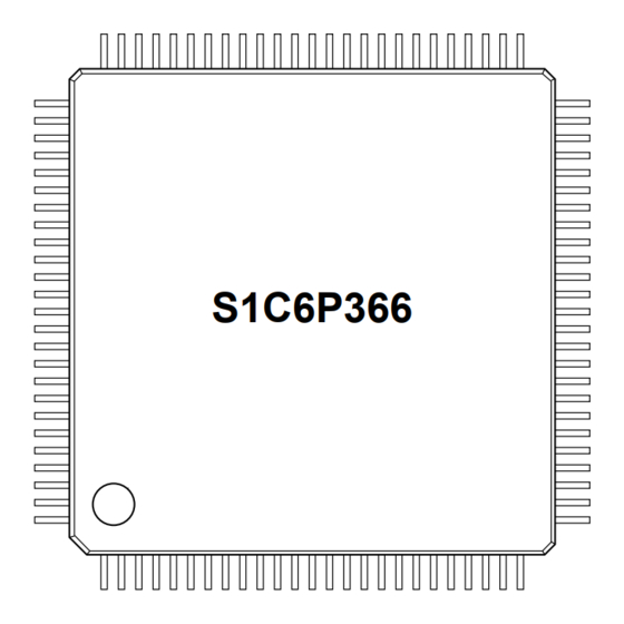
Page 13: Pin Layout Diagram
SEG26 TEST TEST SEG1 SEG1 SEG27 SEG27 SEG2 SEG2 SEG28 SEG28 SEG3 SEG3 SEG29 SEG29 SEG4 SEG4 SEG30 SEG30 N.C. SEG5 SEG5 SEG31 SEG31 N.C. SEG6 SEG6 N.C. : No Connection Fig. 1.3.1 Pin layout diagram EPSON S1C6P366 TECHNICAL MANUAL... -
Page 14: Pin Description
Serial clock input/output pin for Flash programming ∗1 CLKIN Clock input pin for Flash programming ∗1 SPRG Control pin for Flash programming ∗1 N.C. in S1C63358 Refer to Chapter 5, "PROM Programmer and Operating Mode", for the Flash programming pins. EPSON S1C6P366 TECHNICAL MANUAL... -
Page 15: Mask Option
Either CR oscillation circuit or ceramic oscillation circuit can be selected as the OSC3 oscillation circuit. Refer to Section 4.3.3, "OSC3 oscillation circuit", for details. The other mask options provided for the S1C63358/63158 are fixed as follows in the S1C6P366, so they cannot be selected. • OSC1 oscillation circuit ......... Crystal oscillation •... -
Page 16: Power Supply And Initial Reset
The S1C6P366 operating power voltage is as follows: 2.7 V to 5.5 V The S1C6P366 operates by applying a single power supply within the above range between V and V . The S1C6P366 itself generates the voltage necessary for all the internal circuits by the built-in power supply circuits shown in Table 2.1.1. -
Page 17: Voltage
Since the power supply voltage of the S1C6P366 is 2.7 V or more, this switching is not necessary and the software control does not affect the operating mode. However, when using the S1C6P366 as a development tool for the S1C63358/63158, the operating mode control routine must be implemented according to the model.For Oscillation Circuit And Internal Circuits -
Page 18: Initial Reset
2.0 msec. In the S1C6P366, a low level input to the reset terminal initializes some analog circuits as well as the internal logic. At this time, 10 µA or more current is consumed as the bias current. -
Page 19: Terminal Settings At Initial Resetting
P40 (Input & high impedance) AD0(I) P41 (Input & high impedance) AD1(I) P42 (Input & high impedance) AD2(I) P43 (Input & high impedance) AD3(I) For setting procedure of the functions, see explanations for each of the peripheral circuits. EPSON S1C6P366 TECHNICAL MANUAL... -
Page 20: Test Terminal (Test)
This is the terminal used for the factory inspection of the IC. During normal operation, connect the TEST terminal to V 2.4 Terminals for Flash EEPROM The S1C6P366 has the following terminals used for writing data to the Flash EEPROM and for factory testing. SPRG:... -
Page 21: Chapter 3 Cpu, Prom, Ram
The core CPU can linearly access the program space up to step FFFFH from step 0000H, however, the program area of the S1C6P366 is step 0000H to step 3FFFH. The program start address after initial reset is assigned to step 0110H. The non-maskable interrupt (NMI) vector and hardware interrupt vectors are allocated to step 0100H and steps 0102H–010EH, respectively. - Page 22 4-bit data. 0000H 4-bit access area (SP2 stack area) 00FFH 0100H 4/16-bit access area (SP1 stack area) 01FFH 0200H 4-bit access area (data area) 07FFH 4 bits Fig. 3.3.1 Configuration of data RAM EPSON S1C6P366 TECHNICAL MANUAL...
-
Page 23: Peripheral Circuits And Operation
IRCUITS AND PERATION The peripheral circuits of the S1C6P366 (timer, A/D, I/O, etc.) are interfaced with the CPU in the memory mapped I/O method. Thus, all the peripheral circuits can be controlled by accessing the I/O memory on the memory map using the memory operation instructions. The following sections explain the detailed operation of each peripheral circuit. - Page 24 SIK20 ∗3 ∗2 – Unused FF28H ∗3 ∗2 – Unused SIK20 Enable Disable K20 interrupt selection register Remarks ∗1 Initial value at initial reset ∗2 Not set in the circuit ∗3 Constantly "0" when being read EPSON S1C6P366 TECHNICAL MANUAL...
- Page 25 SIF is selected FF44H IOC11 Output Input P11 I/O control register (ESIF=0) functions as a general-purpose register when SIF is selected IOC10 Output Input P10 I/O control register (ESIF=0) functions as a general-purpose register when SIF is selected EPSON S1C6P366 TECHNICAL MANUAL...
- Page 26 A/D is enabled IOC40 Output Input P40 I/O control register (PAD0=0) functions as a general-purpose register when A/D is enabled PUL43 PUL43 PUL42 PUL41 PUL40 PUL42 General-purpose register FF51H PUL41 PUL40 EPSON S1C6P366 TECHNICAL MANUAL...
- Page 27 Timer 0 pulse polarity selection (for event counter mode) CHSEL Timer1 Timer0 TOUT output channel selection CHSEL PTOUT CKSEL1 CKSEL0 PTOUT TOUT output control FFC1H CKSEL1 OSC3 OSC1 Prescaler 1 source clock selection CKSEL0 OSC3 OSC1 Prescaler 0 source clock selection EPSON S1C6P366 TECHNICAL MANUAL...
- Page 28 ADDR3 ADDR2 ADDR1 ADDR0 ∗2 ADDR2 – A/D converted data (D0–D3) FFD2H ∗2 ADDR1 – ∗2 ADDR0 – ∗2 ADDR7 – ADDR8 ADDR6 ADDR5 ADDR4 ∗2 ADDR6 – A/D converted data (D4–D7) FFD3H ∗2 ADDR5 – ∗2 ADDR4 – EPSON S1C6P366 TECHNICAL MANUAL...
- Page 29 Interrupt factor flag (Clock timer 8 Hz) Reset Invalid Interrupt factor flag (Clock timer 16 Hz) ∗3 ∗2 – Unused ∗3 ∗2 – Unused FFF7H ∗3 ∗2 – Unused Reset Invalid Interrupt factor flag (A/D converter) EPSON S1C6P366 TECHNICAL MANUAL...
-
Page 30: Watchdog Timer
4.2.1 Configuration of watchdog timer The S1C6P366 has a built-in watchdog timer that operates with a 256 Hz divided clock from the OSC1 as the source clock. The watchdog timer starts operating after initial reset, however, it can be stopped by the software. -
Page 31: I/O Memory Of Watchdog Timer
(1) When the watchdog timer is being used, the software must reset it within 3-second cycles. (2) Because the watchdog timer is set in operation state by initial reset, set the watchdog timer to disabled state (not used) before generating an interrupt (NMI) if it is not used. EPSON S1C6P366 TECHNICAL MANUAL... -
Page 32: Oscillation Circuit
4.3.1 Configuration of oscillation circuit The S1C6P366 has two oscillation circuits (OSC1 and OSC3). OSC1 is a crystal oscillation circuit that supplies the operating clock to the CPU and peripheral circuits. OSC3 is either a CR or a ceramic oscilla- tion circuit. -
Page 33: Osc3 Oscillation Circuit
CHAPTER 4: PERIPHERAL CIRCUITS AND OPERATION (Oscillation Circuit) 4.3.3 OSC3 oscillation circuit The S1C6P366 has built-in the OSC3 oscillation circuit that generates the CPU's sub-clock for high speed operation and the source clock for peripheral circuits needing a high speed clock (programmable timer, FOUT output). -
Page 34: Operating Voltage
V voltage level. When using the S1C6P366 as a development tool for the S1C63358/63158, switch the operating voltage using the VDC register according to the control sequence of the model (refer to the "Technical Manual"). Furthermore, internal logic circuits (including the OSC3 oscillation circuit) of the S1C6P366 except for the... -
Page 35: I/O Memory Of Oscillation Circuit
CLKCHG register that switches the CPU clock. When using the S1C6P366 as a development tool for the S1C63358/63158, switch the operating voltage using this register according to the control sequence of the model (refer to the "Technical Manual"). -
Page 36: Programming Notes
CPU clock cannot be switched from OSC1 to OSC3 using the CLKCHG register if the VDC register value is "0". When using the S1C6P366 as a development tool for the S1C63358/63158, switch the operating voltage using the VDC register according to the control sequence of the model (refer to the "Technical Manual"). -
Page 37: Input Ports (K00-K03, K10-K13 And K20)
4.4 Input Ports (K00–K03, K10–K13 and K20) 4.4.1 Configuration of input ports The S1C6P366 has nine bits of general-purpose input ports. Each of the input port terminals (K00–K03, K10–K13, K20) provides internal pull-up resistor. Figure 4.4.1.1 shows the configuration of input port (K00–K03, K10–K13). -
Page 38: Interrupt Function
Fig. 4.4.2.1 Input interrupt circuit configuration (K00–K03, K10–K13) Address Address Input comparison Interrupt factor register (KCP20) Interrupt flag (IK2) request Address Interrupt mask Interrupt selection register (EIK2) register (SIK20) Address Address Fig. 4.4.2.2 Input interrupt circuit configuration (K20) EPSON S1C6P366 TECHNICAL MANUAL... -
Page 39: Mask Option
Further, terminals that have been masked for interrupt do not affect the conditions for interrupt generation. 4.4.3 Mask option In the S1C6P366, the input port specification is fixed at "Input with pull-up resistor". EPSON S1C6P366 TECHNICAL MANUAL... -
Page 40: I/O Memory Of Input Ports
∗2 – Unused ∗3 ∗2 – Unused FFF5H Interrupt factor flag (K20) Reset Invalid Interrupt factor flag (K10–K13) *1 Initial value at initial reset *2 Not set in the circuit *3 Constantly "0" when being read EPSON S1C6P366 TECHNICAL MANUAL... - Page 41 When "0" is written: Mask Reading: Valid With these registers, masking of the input port interrupt can be selected for each of the three systems (K00–K03, K10–K13, K20). At initial reset, these registers are set to "0". EPSON S1C6P366 TECHNICAL MANUAL...
- Page 42 The software can discriminates which key was pressed from the conversion result. After that, turn SENON off to reduce current consumption. Output SENON register Generate an interrupt A/D IN Key set Fig. 4.4.4.1 Key position sensing circuit EPSON S1C6P366 TECHNICAL MANUAL...
-
Page 43: Programming Notes
"1") is set or the RETI instruction is executed unless the interrupt factor flag is reset. Therefore, be sure to reset (write "1" to) the interrupt factor flag in the interrupt service routine before shifting to the interrupt enabled state. EPSON S1C6P366 TECHNICAL MANUAL... -
Page 44: Output Ports (R00-R03, R10-R13 And R20-R23)
When using the output port (R02, R03) as the special output port, the data register must be fixed at "1" and the high impedance control register must be fixd at "0" (data output). 4.5.2 Mask option In the S1C6P366, output specifications of all the output ports are fixed at complementary output. EPSON S1C6P366 TECHNICAL MANUAL... -
Page 45: High Impedance Control
R02 and R03 registers when the special output has been selected. • Be aware that the output terminal shifts into high impedance status when "1" is written to the high impedance control register (R02HIZ, R03HIZ). EPSON S1C6P366 TECHNICAL MANUAL... - Page 46 Note: A hazard may occur when the FOUT signal is turned ON and OFF. Figure 4.5.4.3 shows the output waveform of the FOUT signal. R03HIZ register Fix at "0" R03 register Fix at "1" FOUTE register "0" "1" "0" FOUT output Fig. 4.5.4.3 Output waveform of FOUT signal EPSON S1C6P366 TECHNICAL MANUAL...
-
Page 47: I/O Memory Of Output Ports
When "1" is written, it shifts into high impedance status. When the output ports R02 and R03 are used for special output (TOUT, FOUT), fix the R02HIZ register and the R03HIZ register at "0" (data output). At initial reset, these registers are set to "0". EPSON S1C6P366 TECHNICAL MANUAL... - Page 48 "0", the TOUT signal is output from the R02 terminal. When "0" is written, the R02 termi- nal goes high (V When using the R02 output port for DC output, fix this register at "0". At initial reset, this register is set to "0". EPSON S1C6P366 TECHNICAL MANUAL...
-
Page 49: Programming Notes
(2) A hazard may occur when the FOUT signal and the TOUT signal are turned ON and OFF. (3) When f is selected for the FOUT signal frequency, it is necessary to control the OSC3 oscillation OSC3 circuit before output. Refer to Section 4.3, "Oscillation Circuit", for the control and notes. EPSON S1C6P366 TECHNICAL MANUAL... -
Page 50: I/O Ports (P00-P03, P10-P13, P20-P23, P30-P33 And P40-P43)
Refer to Section 4.11, "A/D Converter", for control of the A/D converter. 4.6.2 Mask option In the S1C6P366, the output specification of all the I/O ports is fixed at "complementary output", and the pull-up option for the P10–P13, P20–P23 and P30–P33 ports is fixed at "with pull-up resistor". -
Page 51: I/O Control Registers And Input/Output Mode
4.6.4 Pull-up during input mode A pull-up resistor that operates during the input mode is built into the I/O ports P10–P13, P20–P23 and P30–P33 of the S1C6P366. The pull-up resistor becomes effective by writing "1" to the pull-up control register PULxx that corre- sponds to each port, and the input line is pulled up during the input mode. -
Page 52: I/O Memory Of I/O Ports
IOC33 IOC32 IOC31 IOC30 IOC32 Output Input P30–P33 I/O control register FF4CH IOC31 Output Input IOC30 Output Input *1 Initial value at initial reset *2 Not set in the circuit *3 Constantly "0" when being read EPSON S1C6P366 TECHNICAL MANUAL... - Page 53 In the slave mode, all the P10–P13 ports are set to the serial interface input/output port. In the master mode, P10–P12 are set to the serial interface input/output port and P13 can be used as the I/O port. At initial reset, this register is set to "0". EPSON S1C6P366 TECHNICAL MANUAL...
- Page 54 Make this waiting time the amount of time or more calculated by the following expression. 10 × C × R C: terminal capacitance 5 pF + parasitic capacitance ? pF R: pull-up resistance 300 k Ω EPSON S1C6P366 TECHNICAL MANUAL...
-
Page 55: Programming Note
Particular care needs to be taken of the key scan during key matrix configuration. Make this waiting time the amount of time or more calculated by the following expression. 10 × C × R C: terminal capacitance 5 pF + parasitic capacitance ? pF R: pull-up resistance 300 kΩ EPSON S1C6P366 TECHNICAL MANUAL... -
Page 56: Lcd Driver (Com0-Com3, Seg0-Seg31)
ALOFF, ALON (all ON) has priority over the ALOFF (all OFF). (2) Setting of drive duty In the S1C6P366, the drive duty can be set to 1/4, 1/3 or 1/2 by the software. This setting is done using the LDUTY1 and LDUTY0 registers as shown in Table 4.7.3.1. - Page 57 CHAPTER 4: PERIPHERAL CIRCUITS AND OPERATION (LCD Driver) LCD lighting status COM0 COM0 COM1 COM2 COM1 COM3 SEG0–31 COM2 Not lit COM3 0–31 Frame frequency Fig. 4.7.3.1 Dynamic drive waveform for 1/4 duty (1/3 bias) EPSON S1C6P366 TECHNICAL MANUAL...
- Page 58 Fig. 4.7.3.2 Dynamic drive waveform for 1/3 duty (1/3 bias) LCD lighting status COM0 COM0 COM1 COM1 SEG0–31 COM2 Not lit COM3 0–31 Frame frequency Fig. 4.7.3.3 Dynamic drive waveform for 1/2 duty (1/3 bias) EPSON S1C6P366 TECHNICAL MANUAL...
- Page 59 CHAPTER 4: PERIPHERAL CIRCUITS AND OPERATION (LCD Driver) (3) Static drive The S1C6P366 provides software setting of the LCD static drive. To set in static drive, write "1" to the common output signal control register STCD. Then, by writing "1" to any one of COM0 to COM3 (display memory) corresponding to the SEG terminal, the SEG terminal outputs a static ON waveform.
-
Page 60: Segment Option
When DC output is selected, either complementary output or N-channel open drain output can be selected for each terminal. ∗ The terminal pairs are combination of SEG2 × n and SEG2 × n + 1 (where n is an integer from 0 to 15). EPSON S1C6P366 TECHNICAL MANUAL... -
Page 61: Mask Option
* < LCD SEGMENT DECODE TABLE > * SEG COM0 COM1 COM2 COM3 SPEC *EOF 4.7.5 Mask option The S1C6P366 generates the LCD drive voltage using the internal power supply circuit and does not allow use of an external power source. EPSON S1C6P366 TECHNICAL MANUAL... -
Page 62: I/O Memory Of Lcd Driver
64 (32 × 2) COM0, COM1 32 Hz 96 (32 × 3) COM0–COM2 42.7 Hz 128 (32 × 4) COM0–COM3 32 Hz ∗ When f = 32.768 kHz OSC1 At initial reset, this register is set to "0". EPSON S1C6P366 TECHNICAL MANUAL... -
Page 63: Programming Notes
(2) 100 msec or more time is necessary for stabilizing the LCD drive voltages V and V after setting the LCD power control register LPWR to "1". Be careful of the segment-on right after the power is turned on. EPSON S1C6P366 TECHNICAL MANUAL... -
Page 64: Clock Timer
4.8 Clock Timer 4.8.1 Configuration of clock timer The S1C6P366 has a built-in clock timer that uses OSC1 (crystal oscillator) as the source oscillator. The clock timer is configured of an 8-bit binary counter that serves as the input clock, f... -
Page 65: Interrupt Function
(EIT0, EIT1, EIT2, EIT3). However, regardless of the interrupt mask register setting, the interrupt factor flag is set to "1" at the falling edge of the corresponding signal. EPSON S1C6P366 TECHNICAL MANUAL... -
Page 66: I/O Memory Of Clock Timer
"0" is written. In the STOP status, the timer data is maintained until the next RUN status or the timer is reset. Also, when the STOP status changes to the RUN status, the data that is maintained can be used for resuming the count. At initial reset, this register is set to "0". EPSON S1C6P366 TECHNICAL MANUAL... -
Page 67: Programming Notes
"1") is set or the RETI instruction is executed unless the interrupt factor flag is reset. Therefore, be sure to reset (write "1" to) the interrupt factor flag in the interrupt service routine before shifting to the interrupt enabled state. EPSON S1C6P366 TECHNICAL MANUAL... -
Page 68: Programmable Timer
4.9.1 Configuration of programmable timer The S1C6P366 has two 8-bit programmable timer systems (timer 0 and timer 1) built-in. Timer 0 and timer 1 are composed of 8-bit presettable down counters and they can be used as 8-bit × 2 channel programmable timers or a 16-bit ×... -
Page 69: Tow Separate 8-Bit Timer (Mode16 = "0") Operation
PTRUN0 (1) PTRST0 (1) RLD00–07 (10–17) Input clock PTD07 (17) PTD06 (16) PTD05 (15) PTD04 (14) PTD03 (13) PTD02 (12) PTD01 (11) PTD00 (10) Preset Reload & Interrupt generation Fig. 4.9.2.1.1 Basic operation timing of down counter EPSON S1C6P366 TECHNICAL MANUAL... -
Page 70: Counter Mode
2,048 Hz signal after changing the input level of the K13 input port terminal. Consequently, the pulse width of noise that can reliably be rejected is 0.48 msec or less.) Figure 4.9.2.2.2 shows the count down timing with noise rejecter. EPSON S1C6P366 TECHNICAL MANUAL... -
Page 71: Setting Of Input Clock In Timer Mode
By writing "1" to the register PTRUN0 (timer 0) or PTRUN1 (timer 1), the prescaler inputs the source clock and outputs the clock divided by the selected division ratio. The counter starts counting down by inputting the clock. EPSON S1C6P366 TECHNICAL MANUAL... -
Page 72: Interrupt Function
ON and OFF by setting the register. Figure 4.9.2.5.3 shows the output waveform of the TOUT signal. R02HIZ register Fix at "0" R02 register Fix at "1" PTOUT register "0" "1" "0" TOUT output Fig. 4.9.2.5.3 Output waveform of the TOUT signal EPSON S1C6P366 TECHNICAL MANUAL... -
Page 73: Transfer Rate Setting For Serial Interface
It continues counting down from the initial value after reloading. In addition to reloading the counter, this underflow signal controls the interrupt generation, pulse (TOUT signal) output and clock supplying to the serial interface. EPSON S1C6P366 TECHNICAL MANUAL... -
Page 74: Counter Mode
2,048 Hz signal after changing the input level of the K13 input port terminal. Consequently, the pulse width of noise that can reliably be rejected is 0.48 msec or less.) Figure 4.9.3.2.2 shows the count down timing with noise rejecter. EPSON S1C6P366 TECHNICAL MANUAL... -
Page 75: Setting Of Input Clock In Timer Mode
Source clock / 1 By writing "1" to the register PTRUN0 (timer 0), the prescaler inputs the source clock and outputs the clock divided by the selected division ratio. The counter starts counting down by inputting the clock. EPSON S1C6P366 TECHNICAL MANUAL... -
Page 76: Interrupt Function
ON and OFF by setting the register. Figure 4.9.3.5.2 shows the output waveform of the TOUT signal. R02HIZ register Fix at "0" R02 register Fix at "1" PTOUT register "0" "1" "0" TOUT output Fig. 4.9.3.5.2 Output waveform of the TOUT signal EPSON S1C6P366 TECHNICAL MANUAL... -
Page 77: Transfer Rate Setting For Serial Interface
A setting value for the RLD1X register according to a transfer rate is calculated by the following expres- sion: RLD1X, RLD0X = fosc / (2 ∗ bps ∗ division ratio of the prescaler) - 1 fosc: Oscillation frequency (OSC1/OSC3) bps: Transfer rate (00H can be set to RLD1X) EPSON S1C6P366 TECHNICAL MANUAL... -
Page 78: I/O Memory Of Programmable Timer
Unused FFF2H IPT1 Interrupt factor flag (Programmable timer 1) IPT0 Reset Invalid Interrupt factor flag (Programmable timer 0) *1 Initial value at initial reset *2 Not set in the circuit *3 Constantly "0" when being read EPSON S1C6P366 TECHNICAL MANUAL... - Page 79 When 16-bit × 1 channel is selected, timer 0 and timer 1 are chained together and are used as a 16-bit programmable timer. The clock is input to timer 0 and interrupts will be generated from timer 1. At initial reset, this register is set to "0". EPSON S1C6P366 TECHNICAL MANUAL...
- Page 80 Since the high-order 4 bits are held by reading the low-order 4 bits, be sure to read the low-order 4 bits first. Since these latches are exclusively for reading, the writing operation is invalid. At initial reset, these counter data are set to "00H". EPSON S1C6P366 TECHNICAL MANUAL...
- Page 81 R02 and when "0" is written, the terminal goes to a high ) level. However, the data register R02 must always be "1" and the high impedance control register R02HIZ must always be "0" (data output state). At initial reset, this register is set to "0". EPSON S1C6P366 TECHNICAL MANUAL...
- Page 82 RETI instruction is executed unless the interrupt factor flag is reset. Therefore, be sure to reset (write "1" to) the interrupt factor flag in the interrupt service routine before shifting to the interrupt enabled state. At initial reset, these flags are set to "0". EPSON S1C6P366 TECHNICAL MANUAL...
-
Page 83: Programming Notes
. Be especially careful when using the OSC1 (low- speed clock) as the clock source of the programmable timer and the CPU is operating with the OSC3 (high-speed clock). EPSON S1C6P366 TECHNICAL MANUAL... -
Page 84: Serial Interface (Sin, Sout, Sclk, Srdy)
The synchronous clock for serial data input/output may be set by selecting by software any one of three types of master mode (internal clock mode: when the S1C6P366 is to be the master for serial input/ output) and a type of slave mode (external clock mode: when the S1C6P366 is to be the slave for serial input/output). -
Page 85: Mask Option
4.10.3 Master mode and slave mode of serial interface The serial interface of the S1C6P366 has two types of operation mode: master mode and slave mode. The master mode uses an internal clock as the synchronous clock for the built-in shift register, and outputs this internal clock from the SCLK (P12) terminal to control the external (slave side) serial device. -
Page 86: Data Input/Output And Interrupt Function
(1) Serial data output procedure and interrupt The S1C6P366 serial interface is capable of outputting parallel data as serial data, in units of 8 bits. By setting the parallel data to the data registers SD0–SD3 (FF72H) and SD4–SD7 (FF73H) and writing "1"... - Page 87 Fig. 4.10.4.1 Serial data input/output permutation (4) SRDY signal When the S1C6P366 serial interface is used in the slave mode (external clock mode), SRDY signal is used to indicate whether the internal serial interface is available to transmit or receive data for the master side (external) serial device.
-
Page 88: I/O Memory Of Serial Interface
At initial reset, this register is set to "0". Note: After setting ESIF to "1", wait at least 10 µsec before starting actual data transfer since a hazard may be generated from the P12 (SCLK) terminal when ESIF is set to "1". EPSON S1C6P366 TECHNICAL MANUAL... - Page 89 Pay attention to the polarity of the synchronous clock selected by the mask option because the selection content is different. The input data fetch timing may be selected but output timing for output data is fixed at the falling edge of SCLK. At initial reset, this register is set to "0". EPSON S1C6P366 TECHNICAL MANUAL...
- Page 90 ) level bit into "0", and is loaded to these registers. Perform data reading only while the serial interface is not running (i.e., the synchronous clock is neither being input or output). At initial reset, these registers are undefined. EPSON S1C6P366 TECHNICAL MANUAL...
-
Page 91: Programming Notes
"1") is set or the RETI instruction is executed unless the interrupt factor flag is reset. Therefore, be sure to reset (write "1" to) the interrupt factor flag in the interrupt service routine before shifting to the interrupt enabled state. EPSON S1C6P366 TECHNICAL MANUAL... -
Page 92: A/D Converter
CHAPTER 4: PERIPHERAL CIRCUITS AND OPERATION (A/D Converter) 4.11 A/D Converter 4.11.1 Characteristics and configuration of A/D converter The S1C6P366 has a built-in A/D converter with the following characteristics. • Conversion method: Successive-approximation type • Resolution: 8 bits Maximum error: ±3 LSB, A/D clock: OSC1, OSC3, V = 2.7 V to 5.5 V... -
Page 93: Mask Option
The analog input terminals of the A/D converter are shared with the I/O port terminals P40–P43. Therefore, the terminal specification of the A/D converter is decided by setting the I/O port mask option. In the S1C6P366, the P40–P43 ports specification is fixed at "without pull-up resistor". 4.11.4 Control of A/D converter... - Page 94 Figure 4.11.4.1 shows the flow chart for starting an A/D conversion. Set PAD0–PAD3 Enable A/D input channel Set CHS1, CHS0 Select A/D input channel Set ADCLK Select A/D input clock Set ADRUN to "1" Start A/D conversion Fig. 4.11.4.1 Flowchart for starting A/D conversion EPSON S1C6P366 TECHNICAL MANUAL...
-
Page 95: Interrupt Function
The interrupt factor flag set in "1" is reset to "0" by writing "1". The interrupt vector for the A/D conversion completion has been set in 010EH. A/D conversion completion Interrupt factor flag Address Interrupt request Interrupt mask register EIAD Address Fig. 4.11.5.1 Configuration of A/D converter interrupt circuit EPSON S1C6P366 TECHNICAL MANUAL... -
Page 96: I/O Memory Of A/D Converter
Reading: Valid When "1" is written to ADCLK, OSC3 is selected as the clock source for the A/D converter. When "0" is written, OSC1 is selected. At initial reset, this register is set to "0" (OSC1). EPSON S1C6P366 TECHNICAL MANUAL... - Page 97 VADSEL: A/D power source selection register (FF01H•D3) In the S1C6P366, the value set in this register does not affect the operating mode (operating voltage) of the A/D converter. However, when using the S1C6P366 as a development tool for the S1C63358/63158, control the operating voltage using this register according to the control sequence of the model (refer to the "Technical Manual").
-
Page 98: Programming Notes
A/D converter (for input/output of digital signals). It affects the A/D conversion precision. (7) In the S1C6P366, the value set in the VADSEL register does not affect the operating mode (operating voltage) of the A/D converter. However, when using the S1C6P366 as a development tool for the S1C63358/63158, control the operating voltage using the VADSEL register according to the control sequence of the model (refer to the "Technical Manual"). -
Page 99: Buzzer Output Circuit
Fig. 4.12.1.1 Configuration of buzzer output circuit 4.12.2 Mask option In the S1C6P366, polarity of the buzzer signal output from the BZ terminal is fixed at negative polarity. The BZ terminal goes to a high (V ) level when the buzzer signal is not output. Drive a piezo buzzer by externally connecting an PNP transistor. -
Page 100: Control Of Buzzer Output
Fig. 4.12.3.2 2 Hz interval Note: Since it generates a buzzer signal that is out of synchronization with the BZON register, hazards may at times be produced when the signal goes ON/OFF due to the setting of the BZON register. EPSON S1C6P366 TECHNICAL MANUAL... -
Page 101: I/O Memory Of Buzzer Output Circuit
4.12.5 Programming note Since it generates a buzzer signal that is out of synchronization with the BZON register, hazards may at times be produced when the signal goes ON/OFF due to the setting of the BZON register. EPSON S1C6P366 TECHNICAL MANUAL... -
Page 102: Svd (Supply Voltage Detection) Circuit
Not allowed Be aware that the SVD circuit in the S1C6P366 does not operate properly if the SVDS register is set to 13 or less, the SVD operation cannot be guaranteed since the lower limit of the operating voltage is 2.7 V. -
Page 103: I/O Memory Of Svd Circuit
(3) Be aware that the SVD circuit in the S1C6P366 does not operate properly if the SVDS register is set to 13 or less, the SVD operation cannot be guaranteed since the lower limit of the operating voltage is 2.7 V. -
Page 104: Interrupt And Halt
NMI are masked and interrupts cannot be accepted until the other one is set. <HALT> The S1C6P366 has HALT functions that considerably reduce the current consumption when it is not necessary. The CPU enters HALT status when the HALT instruction is executed. - Page 105 KCP10 SIK10 KCP11 Interrupt factor flag SIK11 Interrupt mask register EIK1 KCP12 Input comparison register SIK12 Interrupt selection register KCP13 SIK13 KCP20 SIK20 EIK2 EIT3 EIT2 EIT1 EIT0 EIAD Fig. 4.14.1 Configuration of the interrupt circuit EPSON S1C6P366 TECHNICAL MANUAL...
-
Page 106: Interrupt Factor
"1") is set or the RETI instruction is executed unless the interrupt factor flag is reset. Therefore, be sure to reset (write "1" to) the interrupt factor flag in the interrupt service routine before shifting to the interrupt enabled state. EPSON S1C6P366 TECHNICAL MANUAL... -
Page 107: Interrupt Mask
High 0104H Programmable timer 0106H Serial interface 0108H K00–K03 input 010AH K10–K13 input, K20 input 010CH Clock timer 010EH A/D converter The four low-order bits of the program counter are indirectly addressed through the interrupt request. EPSON S1C6P366 TECHNICAL MANUAL... -
Page 108: I/O Memory Of Interrupt
EIAD ∗3 ∗2 – Unused FFE7H ∗3 ∗2 – Unused EIAD Enable Mask Interrupt mask register (A/D converter) *1 Initial value at initial reset *2 Not set in the circuit *3 Constantly "0" when being read EPSON S1C6P366 TECHNICAL MANUAL... - Page 109 Refer to Section 4.4, "Input Ports". EIT3–EIT0: Interrupt mask registers (FFE6H) IT3–IT0: Interrupt factor flags (FFF6H) Refer to Section 4.8, "Clock Timer". EIAD: Interrupt mask register (FFE7H•D0) IAD: Interrupt factor flag (FFF7H•D0) Refer to Section 4.11, "A/D Converter". EPSON S1C6P366 TECHNICAL MANUAL...
-
Page 110: Programming Notes
Further, when re-setting the stack pointer, the SP1 and SP2 must be set as a pair. When one of them is set, all the interrupts including NMI are masked and interrupts cannot be accepted until the other one is set. EPSON S1C6P366 TECHNICAL MANUAL... -
Page 111: Prom P Rogramming And
ROGRAMMING AND PERATING The S1C6P366 has built-in Flash EEPROMs as the code PROM and the segment option PROM that allow the developer to program the PROM data using the exclusive PROM writer (Universal ROM Writer II (S5U1C88000W1)). This chapter explains the PROM programmer that controls data writing and the writing mode. - Page 112 CHAPTER 5: PROM PROGRAMMING AND OPERATING MODE SPRG, RXD, CLKIN 330 kΩ PORT 2 kΩ PORT SCLK PULL_UP 330 kΩ PORT DATA_IN PORT_READ Fig. 5.1.2 Terminal specifications EPSON S1C6P366 TECHNICAL MANUAL...
-
Page 113: Operating Mode
CHAPTER 5: PROM PROGRAMMING AND OPERATING MODE 5.2 Operating Mode Three operating modes are available in the S1C6P366: one is for normal operation and the others are for programming. The operating mode is decided by the terminal setting at power-on or initial reset. -
Page 114: Parallel Programming Mode
CHAPTER 5: PROM PROGRAMMING AND OPERATING MODE 5.2.3 Parallel programming mode The parallel programming can be performed by installing the S1C6P366 to the exclusive PROM writer via the adaptor socket. In this mode, it is not necessary to set up the programming terminals since it is controlled by the exclusive PROM writer. -
Page 115: Differences From Mask Rom Models
6.1 Differences from S1C63358 6.1.1 Terminal configuration The S1C6P366 uses the same package (QFP15-100pin) as the S1C63358. Since the terminals for the PROM programmer added to the S1C6P366 are assigned to the unused terminals of the S1C63358, the terminal assignment is compatible with the S1C63358. -
Page 116: Mask Option
For the LCD segment specifications, both the segment allocation and the output specification can be selected similarly to the S1C63358. Create segment option data using the segment option generator SOG63358 and write it to the segment option PROM in the S1C6P366. The selected option specifications are automatically set to each segment terminal. -
Page 117: Power Supply
S1C6P366: 2.7 V to 5.5 V S1C63358: 0.9 V to 3.6 V The S1C6P366 cannot operate with a less than 2.7 V supply voltage. Note that this difference affects the electrical characteristics. Operating mode of oscillation system voltage regulator and internal operating voltage... - Page 118 . (V = 1/2•V = 3/2•V Furthermore, the LCD drive bias option is fixed at 1/3 bias in the S1C6P366. Therefore, the 1/2 bias = 2•V ) drive allowed in the S1C63358 cannot be evaluated. Operating mode of A/D converter power supply...
-
Page 119: Initial Reset
6.1.5 PROM, RAM The S1C6P366 employs a Flash EEPROM for the internal PROM. The Flash EEPROM can be rewritten up to 100 times. Rewriting data is done at the user's own risk. Table 6.1.5.1 lists the code PROM and RAM sizes of the S1C6P366 and the S1C63358. -
Page 120: Svd Circuit
2.68 2.50 2.70 2.90 SVDS3–0 = "15" 2.42 2.60 2.78 2.60 2.80 3.00 Be aware that the SVD circuit in the S1C6P366 does not operate properly if the SVDS register is set to 13 or less. EPSON S1C6P366 TECHNICAL MANUAL... -
Page 121: Differences From S1C63158
The design of the S1C6P366 is based on the S1C63358, therefore the terminal configuration and assign- ment are different from those of the S1C63158 (e.g., the S1C6P366 has LCD driver output terminals that do not exist in the S1C63158). Furthermore, PROM programming terminals are added to the S1C6P366. - Page 122 – (∗1) SEG6 – – SEG31 – – – – (∗1) CLKIN – – (∗1) SCLK – – (∗1) ∗1: Pin for serial programming ∗2: Test signal monitor pad (Not used when writing; keep it open) EPSON S1C6P366 TECHNICAL MANUAL...
-
Page 123: Mask Option
CHAPTER 6: DIFFERENCES FROM MASK ROM MODELS 6.2.2 Mask option The S1C6P366 cannot specify the S1C63158 mask options individually. The following option combination is provided for the S1C6P366. Table 6.2.2.1 Combination of mask options Mask option S1C6P366E (Type E) S1C6P366F (Type F) OSC1 oscillation circuit Crystal (32.768 kHz) -
Page 124: Power Supply
S1C6P366: 2.7 V to 5.5 V S1C63158: 0.9 V to 3.6 V The S1C6P366 cannot operate with less than 2.7 V supply voltage. Note that this difference affects the electrical characteristics. Operating mode of oscillation system voltage regulator and internal operating voltage... -
Page 125: Initial Reset
CHAPTER 6: DIFFERENCES FROM MASK ROM MODELS LCD system voltage circuit The S1C6P366 has a built-in LCD system voltage circuit that generates the LCD drive voltage. The S1C63158 does not contain this circuit. Operating mode of A/D converter power supply... -
Page 126: Prom, Ram
2.55 2.50 2.70 2.90 SVDS3–0 = "15" 2.55 2.60 2.65 2.60 2.80 3.00 Be aware that the SVD circuit in the S1C6P366 does not operate properly if the SVDS register is set to 13 or less. EPSON S1C6P366 TECHNICAL MANUAL... -
Page 127: Summary Of Notes
UMMARY OF OTES 7.1 Notes for Low Current Consumption The S1C6P366 contains control registers for each of the circuits so that current consumption can be reduced. These control registers reduce the current consumption through programs that operate the circuits at the minimum levels. -
Page 128: Summary Of Notes By Function
NMI are masked again until the other is re-set. Therefore, the settings of SP1 and SP2 must be done as a pair. (4) The S1C6P366 has a built-in code PROM and RAM larger than those of the S1C63358 and the S1C63158. When using the S1C6P366 as a development tool of for the S1C63358/63158, pay attention to the memory size. - Page 129 4 bits (PTD00–PTD03, PTD10–PTD13). For the 16 bit × 1 mode, be sure to read as following sequence: (PTD00–PTD03) → (PTD04–PTD07) → (PTD10–PTD13) → (PTD14–PTD17) The read sequence time should be within 1.46 msec. EPSON S1C6P366 TECHNICAL MANUAL...
- Page 130 Supply trigger only once every time the serial interface is placed in the RUN state. Refrain from performing trigger input multiple times, as leads to malfunctioning. Moreover, when the synchronous clock SCLK is external clock, start to input the external clock after the trigger. EPSON S1C6P366 TECHNICAL MANUAL...
- Page 131 (3) Be aware that the SVD circuit in the S1C6P366 does not operate properly if the SVDS register is set to 13 or less, the SVD operation cannot be guaranteed since the lower limit of the operating voltage is 2.7 V.
- Page 132 LCD segment opotion is done at the user's own risk. (3) The Flash EEPROM data can be rewritten up to 100 times for both the code and segment option PROMs. Rewriting data is done at the user's own risk. EPSON S1C6P366 TECHNICAL MANUAL...
-
Page 133: Precautions On Mounting
In particular, the V –V voltages affect the display quality. Do not connect anything to the V –V terminals when the LCD driver is not used. EPSON S1C6P366 TECHNICAL MANUAL... - Page 134 (1) Design the product and implement the IC on the board so that it is shielded from visible radiation in actual use. (2) The inspection process of the product needs an environment that shields the IC from visible radiation. (3) As well as the face of the IC, shield the back and side too. EPSON S1C6P366 TECHNICAL MANUAL...
-
Page 135: Basic External Wiring Diagram
Resistor for OSC3 CR oscillation 91 kΩ (1.8 MHz/3.0 V) 0.2 µF –C Capacitor 3.3 µF Capacitor 0.1 µF RESET terminal capacitor Note: The above table is simply an example, and is not guaranteed to work. EPSON S1C6P366 TECHNICAL MANUAL... - Page 136 Resistor for OSC3 CR oscillation 91 kΩ (1.8 MHz/3.0 V) 0.2 µF –C Capacitor 3.3 µF Capacitor 0.1 µF RESET terminal capacitor Note: The above table is simply an example, and is not guaranteed to work. EPSON S1C6P366 TECHNICAL MANUAL...
- Page 137 Resistor for OSC3 CR oscillation 91 kΩ (1.8 MHz/3.0 V) 0.2 µF –C Capacitor 3.3 µF Capacitor 0.1 µF RESET terminal capacitor Note: The above table is simply an example, and is not guaranteed to work. EPSON S1C6P366 TECHNICAL MANUAL...
- Page 138 Resistor for OSC3 CR oscillation 91 kΩ (1.8 MHz/3.0 V) 0.2 µF –C Capacitor 3.3 µF Capacitor 0.1 µF RESET terminal capacitor Note: The above table is simply an example, and is not guaranteed to work. EPSON S1C6P366 TECHNICAL MANUAL...
-
Page 139: Chapter Electrical Characteristics
CHAPTER LECTRICAL HARACTERISTICS Note: The electrical characteristics of the S1C6P366 are different from those of the S1C63358/63158. The following characteristic values should be used as reference values when the S1C6P366 is used as a development tool. 9.1 Absolute Maximum Rating... -
Page 140: Dc Characteristics
Low level output current (2) =0.1·V µA Common output current -0.05V COM0–3 µA +0.05V µA Segment output current -0.05V SEG0–31 µA (during LCD output) +0.05V µA Segment output current =0.9·V SEG0–31 -660 µA (during DC output) =0.1·V EPSON S1C6P366 TECHNICAL MANUAL... -
Page 141: Analog Circuit Characteristics And Power Current Consumption
=0V, Ta=-25 to 75°C Item Symbol Condition Min. Typ. Max. Unit Resolution ≤5.5V Fconv=OSC3/2 or OSC1 Error 3.6V≤V ≤3.6V Fconv=OSC3/2 or OSC1 2.7V≤V µs Convertion time conv Fconv=OSC3/2=2MHz 10.5 µs Fconv=OSC1=32kHz Input voltage Reference voltage resistance kΩ EPSON S1C6P366 TECHNICAL MANUAL... -
Page 142: Oscillation Characteristics
The oscillation characteristics change depending on the conditions (components used, board pattern, etc.). Use the following characteristics as reference values and evaluate the characteristics on the actual product. = 3.0 V = 0 V Ta = 25°C Typ. value Resistor value for CR oscillation R [kΩ] EPSON S1C6P366 TECHNICAL MANUAL... -
Page 143: Serial Interface Ac Characteristics
=0V, Ta=25°C, V =0.8V =0.2V =0.8V =0.2V Item Symbol Min. Typ. Max. Unit Transmitting data output delay time Receiving data input set-up time Receiving data input hold time <Master mode> SCLK OUT SOUT <Slave mode> SCLK IN SOUT EPSON S1C6P366 TECHNICAL MANUAL... -
Page 144: Timing Chart
CPU clock cannot be switched from OSC1 to OSC3 using the CLKCHG register if the VDC register value is "0". Set the VDC register to "1" before switching the CPU clock from OSC1 to OSC3 in the S1C6P366. When using the S1C6P366 as a development tool for the S1C63358/63158, switch the operating voltage using the VDC register according to the control sequence of the model (refer to the "Technical... -
Page 145: Characteristics Curves (Reference Value)
This graph is provided only for reference and the characteristic varies according to mounting conditions, parts used and the measurement environment. The output terminals should be used within the rated value of permissible total output current. EPSON S1C6P366 TECHNICAL MANUAL... - Page 146 OSC1: 32.768kHz crystal oscillation, Ta =25°C, V = 0V, no panel load, C = 25pF, C = 100pF, –C = 0.2µF This graph is provided only for reference and the characteristic varies according to mounting conditions, parts used and the measurement environment. EPSON S1C6P366 TECHNICAL MANUAL...
- Page 147 OSC1: 32.768kHz crystal oscillation, Ta =25°C, V = 0V, no panel load, C = 25pF, C = 100pF This graph is provided only for reference and the characteristic varies according to mounting conditions, parts used and the measurement environment. EPSON S1C6P366 TECHNICAL MANUAL...
- Page 148 OSC1: 32.768kHz crystal oscillation, Ta =25°C, V = 0V, no panel load, C = 25pF, C = 100pF This graph is provided only for reference and the characteristic varies according to mounting conditions, parts used and the measurement environment. EPSON S1C6P366 TECHNICAL MANUAL...
-
Page 149: Chapter 10 Package
CHAPTER 10: PACKAGE 10 P CHAPTER ACKAGE 10.1 Plastic Package QFP15-100pin (Unit: mm) ±0.4 ±0.1 INDEX +0.1 0.18 –0.05 +0.05 0.125 –0.025 0° 10° ±0.2 The dimensions are subject to change without notice. EPSON S1C6P366 TECHNICAL MANUAL... -
Page 150: Chapter 11 Pad Layout
CHAPTER 11: PAD LAYOUT 11 P CHAPTER AYOUT 11.1 Diagram of Pad Layout (0, 0) 5.80 mm Chip thickness: 400 µm Pad opening: 98 µm EPSON S1C6P366 TECHNICAL MANUAL... -
Page 151: Pad Coordinates
-2,757 1,482 OSC1 -2,759 2,759 1,625 SEG11 -2,757 1,357 OSC2 -2,759 2,759 1,823 SEG12 -2,757 1,125 -2,759 2,759 2,021 SEG13 -2,757 1,000 OSC3 -2,759 2,759 2,219 SEG14 -2,757 OSC4 -2,759 2,759 2,417 N.C. : No Connection EPSON S1C6P366 TECHNICAL MANUAL... -
Page 152: Appendixa Prom Programming
A PROM P APPENDIX ROGRAMMING A.1 Outline of Writing Tools The following tools are provided for writing user data to the Flash EEPROM built into the S1C6P366. Select one according to the development environment. (1) Serial programing (S1C88/S1C63 Serial Connector) System environment •... -
Page 153: Serial Programming (S1C88/S1C63 Serial Connector)
Execute the SDCP366 to create the segment option PROM HEX data file (C3xxxyyy.OSA) from a segment option document file (C3xxxyyy.SDC). Segment option document file C3xxxyyy.SDC C>SDCP366 Execute Segment Option Data Converter C3xxxyyy.OSA Segment option PROM HEX data file Fig. A.2.1.2 Segment option data converter execution flow EPSON S1C6P366 TECHNICAL MANUAL... - Page 154 The S5U1C6P366Y1 package contains the following files: • SDCP366.EXE (Segment Option Data Converter executable file) • CP366SEG.SDC (Recommended segment option document file) • CP366SEG.OSA (Recommended segment option PROM HEX data file) Refer to Section 4.7.4 "Segment option", for recommended segment option. EPSON S1C6P366 TECHNICAL MANUAL...
-
Page 155: System Connection And Setup For Serial Programming (S1C88/S1C63 Serial Connector)
SW3 to SW8 down. located at the back panel of the Univer- 1 2 3 4 5 6 7 8 sal Writer has been set as in Figure D S W A.2.2.2 (factory setting). Fig. A.2.2.2 DIP switch settings EPSON S1C6P366 TECHNICAL MANUAL... -
Page 156: Serial Programming Procedure (S1C88/S1C63 Serial Connector)
• Double-click the RW63P366.EXE icon. When the control software starts up, the following message is displayed. UNIVERSAL ROM WRITER Ver. 3.xx (C)COPYRIGHT 200x SEIKO EPSON CORPORATION LOADING 63P366 FIRMWARE PROGRAM Ver. 3.xx ..After displaying the message, a prompt as below is displayed. - Page 157 Notes: • Inspection data is written to the PROM at shipment, so erase it once to initialize the contents. • The PROM is protected when user data is written at Seiko Epson's factory. The protection is released after the contents have been erased by the FERSA command.
-
Page 158: Connection Diagram For Serial Programming (S1C88/S1C63 Serial Connector)
Notes: • Do not turn on the power of the target board since the PROM programming power (5 V) is supplied from the Universal Writer. • Since PROM programming uses a 5-V power source, exercise care to the voltage ratings of the parts on the target board. EPSON S1C6P366 TECHNICAL MANUAL... - Page 159 Note: The above table is simply an example, and is not guaranteed to work. Fig. A.2.4.2 Sample connection diagram for serial programming (S1C88/S1C63 Serial Connector) • In the serial programming mode, the power for the S1C6P366 is supplied from the V pin of the S1C88/S1C63 Serial Connector.
-
Page 160: Parallel Programming
Execute the SDCP366 to create the segment option PROM HEX data file (C3xxxyyy.OSA) from a segment option document file (C3xxxyyy.SDC). Segment option document file C3xxxyyy.SDC C>SDCP366 Execute Segment Option Data Converter C3xxxyyy.OSA Segment option PROM HEX data file Fig. A.3.1.2 Segment option data converter execution flow EPSON S1C6P366 TECHNICAL MANUAL... - Page 161 The S5U1C6P366Y1 package contains the following files: • SDCP366.EXE (Segment Option Data Converter executable file) • CP366SEG.SDC (Recommended segment option document file) • CP366SEG.OSA (Recommended segment option PROM HEX data file) Refer to Section 4.7.4 "Segment option", for recommended segment option. EPSON S1C6P366 TECHNICAL MANUAL...
-
Page 162: System Connection And Setup For Parallel Programming
Note: Secure the RS-232C cable with the connector screws to prevent malfunction. (4) Installing the S1C6P366 Adapter Socket Install the S1C6P366 Adapter Socket to the top connector of the Universal Writer. There is a projection on the S1C6P366 Adapter Socket connector to prevent improper insertion. Line up the S1C6P366 Adapter Socket to fit to the notch of the Universal Writer connector. -
Page 163: Parallel Programming Procedure
• Double-click the RW63P366.EXE icon. When the control software starts up, the following message is displayed. UNIVERSAL ROM WRITER Ver. 3.xx (C)COPYRIGHT 200x SEIKO EPSON CORPORATION LOADING 63P366 FIRMWARE PROGRAM Ver. 3.xx ..After displaying the message, a prompt as below is displayed. - Page 164 Remove the S1C6P366 after checking that writing has finished normally. To continue writing, repeat from step (7) to step (10). Note: Do not remove the S1C6P366 when the READY LED on the S1C6P366 Adapter Socket is not lit to prevent destruction.
- Page 165 ERROR". In this case, turn the Universal Writer off once and then turn on before starting up the control software. (12) Power off Turn the Universal Writer off (POWER SW is located at the side panel) then the personal computer. EPSON S1C6P366 TECHNICAL MANUAL...
-
Page 166: Universal Rom Writer Ii (S5U1C88000W1) Specifications
These pins are connected to the V , TXD, RXD, CLK, SCLK and the CLK,SCLK,V signals in the SIO interface. Rear DIP switch This switch is used to set the transmission rate. It has been set to 9600 bps at the factory. EPSON S1C6P366 TECHNICAL MANUAL... -
Page 167: Detailed Description Of The Universal Rom Writer Ii Commands
/V ....Verifies data from the code PROM start address after reading. Description: The contents of the code PROM in the S1C6P366 on the socket are read to the buffer RAM in the PROM writer. The accessed code PROM address is displayed during reading. - Page 168 Operation: Description: Verifies the contents of the code PROM in the S1C6P366 on the socket and the contents of the buffer RAM in the PROM writer. The accessed code PROM address is displayed during verification. When an error occurs, verification stops. At this time, the address and data of the code PROM and the buffer RAM data are displayed.
- Page 169 /V ....Verifies data from the code PROM start address after writing. Description: The buffer RAM data in the PROM writer is written to the S1C6P366 code PROM on the target board connected to the PROM writer. The accessed code PROM address is displayed during writing.
- Page 170 Operation: Description: Verifies the contents of the S1C6P366 code PROM on the target board connected to the PROM writer and the contents of the buffer RAM in the PROM writer. The accessed code PROM address is displayed during verification. When an error occurs, verification stops. At this time, the address and data of the code PROM and the buffer RAM data are displayed.
- Page 171 24 PROTECT command for serial programming Operation: FPROTECT Description: Sets the protect bit of the S1C6P366 PROM on the target board connected to the PROM writer. When the protect bit has been set, execution of all the commands except for FERSA are disabled.
- Page 172 F0 F1 F2 F3 F4 F5 F6 F7 F8 F9 FA FB FC FD FE FF 00010 FF FF FF FF FF FF FF FF FF FF FF FF FF FF FF FF 000F0 FF FF FF FF FF FF FF FF FF FF FF FF FF FF FF FF EPSON S1C6P366 TECHNICAL MANUAL...
- Page 173 ....The macro file C3358.MAC is loaded and the commands MAC_c3358.mac included in the file are executed. When the file contains the commands indicated at the left, LI_c3358001 the code PROM data is loaded and written to the code PROM. EPSON S1C6P366 TECHNICAL MANUAL...
- Page 174 C> ....Returns to DOS. C>EXIT 63P366: ..Entering EXIT returns to the program. 36 HELP command Operation: HELP Description: Command list is displayed. 37 QUIT command Operation: Description: Terminates the program and returns to DOS. EPSON S1C6P366 TECHNICAL MANUAL...
-
Page 175: List Of Commands
Enter key. • A parameter enclosed by [ ] can be omitted. • Loading and saving file names must not include extension. • , indicates selection item. • Logging and macro file names must include extension. EPSON S1C6P366 TECHNICAL MANUAL... -
Page 176: Universal Rom Writer Ii Error Messages
The PROM writer sent NAK to the host computer. The host computer sent NAK to the PROM writer. The S1C6P366 on the target board does not respond or sent NAK to the COMMUNICATION ERROR 2 PROM writer. The S1C6P366 on the target board returns an incorrect command when a COMMUNICATION ERROR 3 command is issued from the PROM writer. -
Page 177: Flash Eeprom Programming Notes
(2) Since PROM programming uses a 5-V power source, be careful of the voltage ratings of the parts on the target board. (3) Make sure that the READY LED on the S1C88/S1C63 Serial Connector or S1C6P366 Adapter Socket is lit when connecting (mounting) or disconnecting (removing) the target board (S1C6P366). -
Page 178: Appendixb S5U1C63000P Manual (Peripheral Circuit Board For S1C63158/358/P366)
These LEDs correspond one-to-one to the registers listed below. The LED lights when the data is logic "1" and goes out when the data is logic "0". VDC, OSCC, CLKCHG, DBON, HLON, VDSEL, VADSEL, SVDS0–3, SVDON, LPWR, VCCHG EPSON S1C6P366 TECHNICAL MANUAL... - Page 179 ∗1 DONE: The monitor pin outputs a high while the LED lights when initialization of this board completes without problems. ∗2 DBON: Used for the S1C63158 and S1C6P366. (5) CR oscillation frequency adjusting control When OSC1 and OSC3 respectively are set for a CR oscillation circuit and a CR/ceramic oscillation circuit by a mask option, this control allows you to adjust the oscillation frequency.
- Page 180 ICE and reset CLK and PRG to the LCLK and the Norm position, respec- tively. Then power on the ICE once again. (10) IOSEL2 When downloading circuit data, set IOSEL2 to the "E" position. Otherwise, set to the "D" position. (11) VC5 Unused. EPSON S1C6P366 TECHNICAL MANUAL...
-
Page 181: Connecting To The Target System
(80-pin/40-pin × 2, 100-pin/50-pin × 2, flat type). Take care when handling the connectors, since they conduct electrical power (V = +3.3 V). mark I/O connection cable CN1-1 (40-pin) CN1-2 (40-pin) CN2-1 (50-pin) CN2-2 (50-pin) To target board Fig. B.2.1 Connecting the S5U1C63000P to the target system EPSON S1C6P366 TECHNICAL MANUAL... - Page 182 Cannot be connected Cannot be connected Cannot be connected Cannot be connected Cannot be connected Cannot be connected ∗ Connectors CN2-1 and CN2-2 are used when the SEG pins are set for DC output with a mask option. EPSON S1C6P366 TECHNICAL MANUAL...
-
Page 183: Usage Precautions
LCD power supply on/off circuit (LPWR) j) LCD constant-voltage change circuit (VCCHG) <Those that can only be counteracted by system or software> k) Current consumed by the internal pull-up resistors l) Input ports in a floating state EPSON S1C6P366 TECHNICAL MANUAL... - Page 184 IC may not have a resonator connected to its OSC3, its emulator can operate with the OSC3 circuit. - Do not turn on the OSC3 oscillation circuit when the voltage-regulating circuit for high-speed operation remains idle. EPSON S1C6P366 TECHNICAL MANUAL...
- Page 185 <Differences in I/O registers> Although the register bit D1 (address FF01H) is always set to 0 when read out, it operates as a read/ write register on this board. Take care to avoid writing a 1 to this bit. EPSON S1C6P366 TECHNICAL MANUAL...
- Page 186 Central Phone: +852-2585-4600 Fax: +852-2827-4346 101 Virginia Street, Suite 290 Telex: 65542 EPSCO HX Crystal Lake, IL 60014, U.S.A. EPSON TAIWAN TECHNOLOGY & TRADING LTD. Phone: +1-815-455-7630 Fax: +1-815-455-7633 10F, No. 287, Nanking East Road, Sec. 3 Northeast Taipei 301 Edgewater Place, Suite 120...
- Page 187 In pursuit of “Saving” Technology, Epson electronic devices. Our lineup of semiconductors, displays and quartz devices assists in creating the products of our customers’ dreams. Epson IS energy savings.
- Page 188 S1C6P366 Technical Manual ELECTRONIC DEVICES MARKETING DIVISION EPSON Electronic Devices Website http://www.epsondevice.com First issue May, 2000 Printed October, 2002 in Japan...
Need help?
Do you have a question about the S1C6P366 and is the answer not in the manual?
Questions and answers