Table of Contents
Advertisement
Quick Links
www.ti.com
User's Guide
DAC63004WCSP-EVM User's Guide
This user's guide describes the characteristics, operation, and use of the DAC63004WCSP-EVM evaluation
module (EVM). This EVM is designed to evaluate the performance of the
commercial, buffered voltage output DACs in a variety of configurations. The DAC63204W, DAC53204W, and
DAC63202W
are also supported by this EVM. Throughout this document, all these devices are referred to
as the DACx3004W, and the terms evaluation board, evaluation module, and EVM are synonymous with
the DAC63004WCSP-EVM. This document includes a schematic, printed-circuit board (PCB) layouts, and a
complete bill of materials.
SLAU879 – DECEMBER 2022
Submit Document Feedback
ABSTRACT
Copyright © 2022 Texas Instruments Incorporated
DAC63004W
and
DAC53004W
DAC63004WCSP-EVM User's Guide
1
Advertisement
Table of Contents

Related Manuals for Texas Instruments DAC63004WCSP-EVM


Summary of Contents for Texas Instruments DAC63004WCSP-EVM
- Page 1 User’s Guide DAC63004WCSP-EVM User's Guide ABSTRACT This user’s guide describes the characteristics, operation, and use of the DAC63004WCSP-EVM evaluation module (EVM). This EVM is designed to evaluate the performance of the DAC63004W DAC53004W commercial, buffered voltage output DACs in a variety of configurations. The DAC63204W, DAC53204W, and DAC63202W are also supported by this EVM.
-
Page 2: Table Of Contents
Figure 2-2. FTDI USB Drivers..............................5 Figure 2-3. Hardware Setup................................ Figure 3-1. DAC63004WCSP-EVM Hardware Simplified Schematic..................Figure 3-2. DAC63004WCSP-EVM High Current Output Stage Block Diagram................. Figure 3-3. DAC63004WCSP-EVM Optional Current Source Circuit Layout................Figure 3-4. DAC63004WCSP-EVM GUI Connection Detection....................Figure 3-5. Interface Settings.............................. -
Page 3: Overview
Table 1-1 details the contents of the EVM kit. Contact the nearest TI Product Information Center if any component is missing. Make sure to verify the latest versions of the related software at the Texas Instruments website, www.ti.com. Table 1-2 lists the optional components not included with the kit. -
Page 4: System Setup
10 operating system. 2.1.2 Software Installation Before software installation, make sure that the DAC63004WCSP-EVM is not connected to the computer. The software can be downloaded from the device product folders. After the software is downloaded, navigate to the download folder, and run the DAC63004WCSP-EVM software installer executable. -
Page 5: Hardware Setup
The software installation also installs the FTDI USB drivers, and automatically copies the required LabVIEW software files and drivers to the computer. The FTDI USB drivers install in a second executable. Figure shows the window that is automatically launched after the DAC63004WCSP-EVM software installation is complete. Figure 2-2. FTDI USB Drivers 2.2 Hardware Setup... -
Page 6: Table 2-1. Dac63004Wcsp-Evm Power Supply
1.8 V to 5.5 V (5 V available from the USB); remove J3 if applying an external VDD to the DAC. J1.1 The jumper settings on the DAC63004WCSP-EVM are crucial to the proper operation of the EVM. Table 2-2 provides the details of the configurable jumper settings on the EVM. -
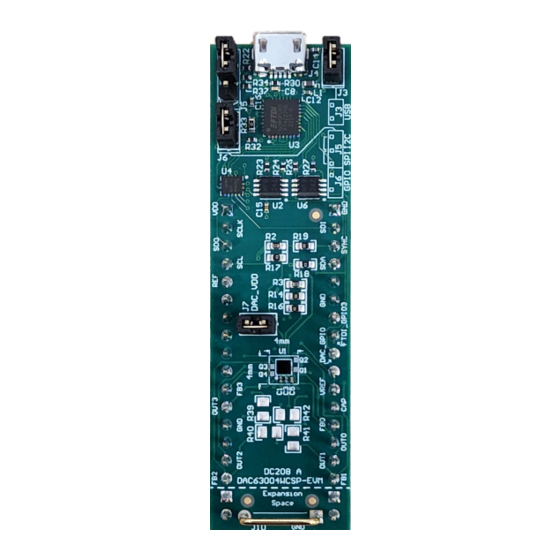
Page 7: Detailed Description
3.1.1 Theory of Operation Figure 3-1 shows a simplified schematic of the DAC63004WCSP-EVM board. There are two 16-pin connectors that provide access to all of the DAC pins. The GPIO, I C, and SPI signals from the onboard controller are connected to the DAC through three level translators. -
Page 8: Table 3-1. Dac63004Wcsp-Evm J1 Pin Definitions
Detailed Description www.ti.com 3.1.1.1 Signal Definitions The DAC63004WCSP-EVM provides access to all DAC pins through connection J1 and J2. Table 3-1 Table 3-2 list the J1 and J2 pin definitions. J8 and J9 provide access to the current outputs when the optional components are populated. -
Page 9: Figure 3-2. Dac63004Wcsp-Evm High Current Output Stage Block Diagram
DAC63004WCSP-EVM. Figure 3-3. DAC63004WCSP-EVM Optional Current Source Circuit Layout Remove R5, R6, R7, and R8 on the DAC63004WCSP-EVM to disconnect the DAC_OUTx and DAC_FBx pins before populating the optional components for the high current output stage. SLAU879 – DECEMBER 2022... -
Page 10: Software Description
The SDO pin on the DACx3004W is connected to the GPIO2 output from the onboard controller. Before configuring the SDO pin as an output to enable readback, remove J6 to disable the GPIO outputs from the onboard controller or remove R13 on the DAC63004WCSP-EVM to disconnect the GPIO2 pin from the SDO pin. DAC63004WCSP-EVM User's Guide SLAU879 –... -
Page 11: Figure 3-6. High Level Configuration Page
Detailed Description 3.2.2 Software Features The DAC63004WCSP-EVM GUI incorporates interactive functions that help configure an individual DACx3004W device using I C or SPI communication. These functions are built into several GUI pages, as shown in the following subsections. The menu bar on the far left of the GUI allows the user to switch between pages. The menu bar displays the High Level Configuration page with Basic DAC, Margining, and Function Generation subpages, and the Low Level Configuration page. -
Page 12: Figure 3-7. Basic Dac Subpage
GPIO pin on the respective DACx3004W device, and control the two GPIO outputs of the DAC63004WCSP-EVM onboard controller. The register settings can be programmed or retrieved using the Program NVM or Reload NVM checkboxes, respectively. -
Page 13: Figure 3-8. Margining Subpage
(Trigger MHx). The register settings are programmed or retrieved using the Program NVM or Reload NVM checkboxes, respectively. Figure 3-8. Margining Subpage SLAU879 – DECEMBER 2022 DAC63004WCSP-EVM User's Guide Submit Document Feedback Copyright © 2022 Texas Instruments Incorporated... -
Page 14: Figure 3-9. Function Generation Subpage
Gen checkboxes start or stop the defined function generation for each channel. The register settings can be programmed or retrieved using the Program NVM or Reload NVM checkboxes, respectively. Figure 3-9. Function Generation Subpage DAC63004WCSP-EVM User's Guide SLAU879 – DECEMBER 2022 Submit Document Feedback Copyright © 2022 Texas Instruments Incorporated... -
Page 15: Figure 3-10. Low Level Configuration Page
Write Selected or Write Modified buttons are pressed. By default, Immediate Update Mode is selected for the Low Level Configuration page write operations. Figure 3-11. Low Level Configuration Page Options SLAU879 – DECEMBER 2022 DAC63004WCSP-EVM User's Guide Submit Document Feedback Copyright © 2022 Texas Instruments Incorporated... -
Page 16: Schematic, Pcb Layout, And Bill Of Materials
This section contains the schematics, printed circuit board (PCB) layout diagrams, and a complete bill of materials for the DAC63004WCSP-EVM. The optional components are shown as do not populate (DNP) on the schematic, and have quantities of zero in the BOM. -
Page 17: Schematics
¡ SPI/I2C Enable 18pF 18pF OE_I2C SH-J3 VCCIO_FTDI OE_GPIO GPIO Enable Decoupling Caps for FTDI422H Level Shifter Enables Figure 4-1. DAC63004WCSP-EVM Schematic Page 1 SLAU879 – DECEMBER 2022 DAC63004WCSP-EVM User's Guide Submit Document Feedback Copyright © 2022 Texas Instruments Incorporated... -
Page 18: Figure 4-2. Dac63004Wcsp-Evm Schematic
DAC_GPIO DAC_GPIO/SDO DAC_A0/SDI 3.32k DAC_SDO DAC_SDI DAC_SDO DAC_SDI DAC_SCL DAC_SDA DAC_SCL DAC_SDA DAC_SCL/SYNC DAC_SDA/SCLK DAC_SYNC DAC_SCLK DAC_SYNC DAC_SCLK Figure 4-2. DAC63004WCSP-EVM Schematic Page 2 DAC63004WCSP-EVM User's Guide SLAU879 – DECEMBER 2022 Submit Document Feedback Copyright © 2022 Texas Instruments Incorporated... -
Page 19: Pcb Layout
Schematic, PCB Layout, and Bill of Materials 4.2 PCB Layout Figure 4-3. DAC63004WCSP-EVM PCB Components Layout SLAU879 – DECEMBER 2022 DAC63004WCSP-EVM User's Guide Submit Document Feedback Copyright © 2022 Texas Instruments Incorporated... -
Page 20: Figure 4-4. Dac63004Wcsp-Evm Pcb Layers
Schematic, PCB Layout, and Bill of Materials www.ti.com Figure 4-4. DAC63004WCSP-EVM PCB Layers DAC63004WCSP-EVM User's Guide SLAU879 – DECEMBER 2022 Submit Document Feedback Copyright © 2022 Texas Instruments Incorporated... -
Page 21: Bill Of Materials
Schematic, PCB Layout, and Bill of Materials 4.3 Bill of Materials Table 4-1. DAC63004WCSP-EVM Bill of Materials Designator Quantity Value Description Package Reference Part Number Manufacturer !PCB Printed Circuit Board DC159 C1, C3 0.1 µF CAP, CERM, 0.1 uF, 6.3 V, +/- 10%, X5R,... - Page 22 Schematic, PCB Layout, and Bill of Materials www.ti.com Table 4-1. DAC63004WCSP-EVM Bill of Materials (continued) Designator Quantity Value Description Package Reference Part Number Manufacturer R29, R31 10 Ω RES, 10.0, 1%, 0.063 W, 0402 0402 RK73H1ETTP10R0F KOA Speer 12 kΩ...
- Page 23 STANDARD TERMS FOR EVALUATION MODULES Delivery: TI delivers TI evaluation boards, kits, or modules, including any accompanying demonstration software, components, and/or documentation which may be provided together or separately (collectively, an “EVM” or “EVMs”) to the User (“User”) in accordance with the terms set forth herein.
- Page 24 www.ti.com Regulatory Notices: 3.1 United States 3.1.1 Notice applicable to EVMs not FCC-Approved: FCC NOTICE: This kit is designed to allow product developers to evaluate electronic components, circuitry, or software associated with the kit to determine whether to incorporate such items in a finished product and software developers to write software applications for use with the end product.
- Page 25 www.ti.com Concernant les EVMs avec antennes détachables Conformément à la réglementation d'Industrie Canada, le présent émetteur radio peut fonctionner avec une antenne d'un type et d'un gain maximal (ou inférieur) approuvé pour l'émetteur par Industrie Canada. Dans le but de réduire les risques de brouillage radioélectrique à...
- Page 26 www.ti.com EVM Use Restrictions and Warnings: 4.1 EVMS ARE NOT FOR USE IN FUNCTIONAL SAFETY AND/OR SAFETY CRITICAL EVALUATIONS, INCLUDING BUT NOT LIMITED TO EVALUATIONS OF LIFE SUPPORT APPLICATIONS. 4.2 User must read and apply the user guide and other available documentation provided by TI regarding the EVM prior to handling or using the EVM, including without limitation any warning or restriction notices.
- Page 27 Notwithstanding the foregoing, any judgment may be enforced in any United States or foreign court, and TI may seek injunctive relief in any United States or foreign court. Mailing Address: Texas Instruments, Post Office Box 655303, Dallas, Texas 75265 Copyright © 2019, Texas Instruments Incorporated...
- Page 28 TI products. TI’s provision of these resources does not expand or otherwise alter TI’s applicable warranties or warranty disclaimers for TI products. TI objects to and rejects any additional or different terms you may have proposed. IMPORTANT NOTICE Mailing Address: Texas Instruments, Post Office Box 655303, Dallas, Texas 75265 Copyright © 2022, Texas Instruments Incorporated...
Need help?
Do you have a question about the DAC63004WCSP-EVM and is the answer not in the manual?
Questions and answers