Table of Contents
Advertisement
Quick Links
This user's guide describes the characteristics, operation, and the use of the DAC8881 evaluation module.
It covers all pertinent areas involved to properly use this EVM board along with the devices that it
supports. The physical PCB layout, schematic diagram, and circuit descriptions are included.
1
1.1
Features
1.2
Power Requirements
1.3
2
2.1
2.2
2.3
3
3.1
3.2
3.3
3.4
3.5
3.6
4
4.1
4.2
4.3
4.4
4.5
.................................................................................................................
5
5.1
5.2
1
Block Diagram
2
Top Silkscreen
3
Layer 1 (Top Signal Plane)
4
Layer 2 (Ground Plane)
5
Layer 3 (Power Plane)
6
Layer 4 (Bottom Signal Plane)
7
Bottom Silkscreen
.................................................................................................................
8
Drill Drawing
9
INL and DNL Characteristic Plots
10
DAC8881 EVM Default Jumper Configuration
11
MMB0 with DAC8881EVM Installed
12
Loading the DAC8881EVM INI file
13
DAC8881 - Frequency/Amplitude and GPIO Control Options
SLAU257A - September 2008 - Revised November 2009
Submit Documentation Feedback
...............................................................................................................
.............................................................................................................
..............................................................................................
..............................................................................................
............................................................................................
.........................................................................................................
.................................................................................................
.....................................................................................................
............................................................................................................
.........................................................................................
........................................................................................
..........................................................................................
.....................................................................................................
..................................................................................................
........................................................................................................
.....................................................................................
..........................................................................................................
...........................................................................................
........................................................................................
....................................................................................
................................................................................................
...............................................................................................................
...............................................................................................................
................................................................................................
....................................................................................................
.....................................................................................................
............................................................................................
...........................................................................................................
.........................................................................................
....................................................................................
......................................................................................
Copyright © 2008-2009, Texas Instruments Incorporated
SLAU257A - September 2008 - Revised November 2009
DAC8881 Evaluation Module
Contents
............................................................
.....................................................
List of Figures
.........................................................................
......................................................
User's Guide
DAC8881 Evaluation Module
2
2
2
3
4
4
8
9
10
10
11
12
13
14
16
16
17
17
18
20
20
21
21
21
4
5
6
6
7
7
8
8
9
11
17
19
19
1
Advertisement
Table of Contents

Related Manuals for Texas Instruments DAC8881


Summary of Contents for Texas Instruments DAC8881
-
Page 1: Table Of Contents
SLAU257A – September 2008 – Revised November 2009 DAC8881 Evaluation Module This user’s guide describes the characteristics, operation, and the use of the DAC8881 evaluation module. It covers all pertinent areas involved to properly use this EVM board along with the devices that it supports. - Page 2 50MHz to communicate with any host microprocessor or DSP-based system. The DAC8881 is designed for unipolar output operation (default mode), but it can also be configured for bipolar output operation with the addition of an external amplifier and some resistors. The option for bipolar mode of operation is included in the EVM with just some minor jumper configuration.
-
Page 3: Evm Overview
DSP, or signal/waveform generator. The headers J2 (top side) and P2 (bottom side) are pass-through connectors provided to allow the control signals and data required to interface a host processor or waveform generator to the DAC8881 EVM using a custom built cable. -
Page 4: Pcb Design And Performance
PCB Layout The DAC8881 EVM is designed to preserve the performance quality of the DAC, device under test, as specified in the datasheet. Carefully analyzing the physical restrictions of the EVM and the given or known elements that contribute to performance degradation of the EVM is key to a successful design implementation. - Page 5 PCB Design and Performance www.ti.com The DAC8881 EVM board is constructed on a four-layer printed circuit board using a copper-clad FR-4 laminate material. The printed circuit board has dimensions of 43,1800 mm (1.7000 inch) × 82,5500 mm (3.2500 inch), and the board thickness is 1,5748 mm (0.062 inch).
- Page 6 PCB Design and Performance www.ti.com Figure 4. Layer 2 (Ground Plane) Figure 5. Layer 3 (Power Plane) DAC8881 Evaluation Module SLAU257A – September 2008 – Revised November 2009 Submit Documentation Feedback Copyright © 2008–2009, Texas Instruments Incorporated...
- Page 7 PCB Design and Performance www.ti.com Figure 6. Layer 4 (Bottom Signal Plane) Figure 7. Bottom Silkscreen SLAU257A – September 2008 – Revised November 2009 DAC8881 Evaluation Module Submit Documentation Feedback Copyright © 2008–2009, Texas Instruments Incorporated...
-
Page 8: Evm Performance
INL and DNL. Figure 9 shows the INL and DNL characteristic plots. DAC8881 Evaluation Module SLAU257A – September 2008 – Revised November 2009 Submit Documentation Feedback Copyright © 2008–2009, Texas Instruments Incorporated... -
Page 9: Bill Of Materials
2200 pF, 0805 ceramic cap, COG, 50V, C2012C0G1H222J 7 × 2 × 2mm terminal strip Samtec TMM-107-01-T-D 3 × 2 × 2mm terminal strip Samtec TMM-103-01-T-D SLAU257A – September 2008 – Revised November 2009 DAC8881 Evaluation Module Submit Documentation Feedback Copyright © 2008–2009, Texas Instruments Incorporated... -
Page 10: Evm Operation
This chapter describes in detail the operation of the EVM to provide guidance to the user in evaluating the on-board DAC and how to interface the EVM to a specific host processor. Refer to the DAC8881 data sheet, (SBAS422) for information about its serial interface and other related topics. -
Page 11: Host Processor Interface
The DAC8881 interfaces with any host processor capable of handling SPI protocols or a popular TI DSP. For more information regarding the DAC8881 data interface, refer to the data sheet (SBAS422). -
Page 12: Digital Control Interface
DAC8881EVM. Either signal can be chosen to drive the DAC8881 chip select (CS) pin. The basic function of the CS and FS signals is to drive the CS pin of the DAC8881 to enable the device communication port and to synchronize the data input into the device immediately following its high-to-low transition. -
Page 13: Analog Output
The EVM includes an external operational amplifier, U2, as an option for other output signal conditioning circuitry for the DAC output. Although the buffered output of the DAC8881 can be monitored through J4 pin 2, the optional external buffer output (if the DAC output is connected to it) can be monitored through the TP3 test point. -
Page 14: Jumper Settings
Jumper Reference Function Setting Routes +5VA for AV and DV to power the analog and digital supplies of the DAC8881. Routes +3.3VA for AV and DV to power the analog and digital supplies of the DAC8881. Routes V to J4-2. - Page 15 J4-6 and J4-8 to the non-inverting input of the U2 op-amp. LDAC1 signal from J2-15 is routed to drive the LDAC signal of the DAC8881. The LDAC signal of the DAC8881 is tied to ground for synchronous update of the DAC8881 output.
-
Page 16: Schematics
DAC input data format is set for twos complement format. If jumper is installed on pins 9 and 10, the RST pin of the DAC8881 is tied to ground so that the DAC is forced into hardware reset mode. - Page 17 12500 TI Boulevard. Dallas, Texas 75243 AVDD = +2.7V to +5.5V Analog VSS = 0V to -15V Analog Title: DAC8881 EVM Engineer: J. PARGUIAN DOCUMENTCONTROL # 6489897 REV: Drawn By: J. PARGUIAN FILE: DATE: SIZE: 1-Apr-2008 SHEET: DAC8881 Rev A.Sch...
-
Page 18: Hardware
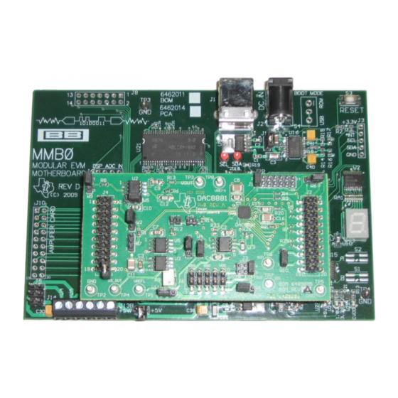
DAC8881EVM must be supplied externally via J14 – a 6 position screw terminal mounted in the lower left corner of the MMB0 board. SLAU257A – September 2008 – Revised November 2009 DAC8881 Evaluation Module Submit Documentation Feedback Copyright © 2008–2009, Texas Instruments Incorporated... -
Page 19: Software - Running Dxp
From left to right, the J14 screw terminal connections are –VA, +VA, +5VA, –5VA, +5VD and GND. The DAC8881 board has power requirements as described in section 1.2 of this manual. The analog power for Vss (–VA) and Vcc (+VA) as well as +5VA may be applied directly to the screw terminals at J14 on the MMB0 (referenced to the GND terminal). -
Page 20: Dxp Gpio Controlled Dac Functions
Reset Pressing the reset button will cause the button to turn ACTIVE and places logic low on pin 17 of the DAC8881. To use this function, please ensure no jumpers are placed on J1 pins 9-10. When the RST pin is low, the device is in hardware reset mode, and the input register and DAC latch are set to the value defined by the RSTSEL pin (refer to the DAC8881EVM Schematic;... -
Page 21: Dac Output Update Options
Timer applies a pulse to the LDAC pin and the output of the DAC8881 is updated synchronously with the falling edge of the applied pulse. Remove the shunt jumper from J1 pins 1-2 and place it on W10 pins 2-3 to use this feature. -
Page 22: Information
Information Related Documentation from Texas Instruments To obtain a copy of any of the following TI documents, call the Texas Instruments Literature Response Center at (800) 477–8924 or the Product Information Center (PIC) at (972) 644–5580. When ordering, identify this manual by its title and literature number. Updated documents also can be obtained through the TI Web site at www.ti.com. - Page 23 Evaluation Board/Kit Important Notice Texas Instruments (TI) provides the enclosed product(s) under the following conditions: This evaluation board/kit is intended for use for ENGINEERING DEVELOPMENT, DEMONSTRATION, OR EVALUATION PURPOSES ONLY and is not considered by TI to be a finished end-product fit for general consumer use. Persons handling the product(s) must have electronics training and observe good engineering practice standards.
- Page 24 IMPORTANT NOTICE Texas Instruments Incorporated and its subsidiaries (TI) reserve the right to make corrections, modifications, enhancements, improvements, and other changes to its products and services at any time and to discontinue any product or service without notice. Customers should obtain the latest relevant information before placing orders and should verify that such information is current and complete.
- Page 25 Mouser Electronics Authorized Distributor Click to View Pricing, Inventory, Delivery & Lifecycle Information: Texas Instruments DAC8881EVM...
Need help?
Do you have a question about the DAC8881 and is the answer not in the manual?
Questions and answers