Table of Contents
Advertisement
Quick Links
www.ti.com
User's Guide
DAC39RF10EVM Evaluation Module
The DAC39RF10EVM is an evaluation board used to evaluate the DAC39RF10, digital-to-analog converters
(DAC) from Texas Instruments.The DAC39RF10 is a family of single and dual channel digital-to-analog converter
(DAC) with 16-bit resolution. The devices can be used as single channel or dual channel non-interpolation
DACs. The device can also be used as interpolating DACs in either direct RF sampling mode or baseband
mode. The maximum input data rate is 20.48 GSPS in single channel mode or 10.24 Gsps in dual channel mode
or baseband mode. The device can generate signals of up to 10, 7.5, and 5 GHz signal bandwidth (8, 12, and
16-bit input resolution) at carrier frequencies exceeding 8 GHz enabling direct sampling through C-band and into
X-band This evaluation board also includes the following important features:
•
Transformer-coupled signal output network allowing a single-ended signal output
with an option to bypass the transformer and use the outputs differentially.
•
The LMX1204 clock chip distributes the DAC sampling clock
•
The LMK04828, clock generator generates SYSREF and FPGA reference clocks for the high-speed serial
interface
•
Transformer-coupled clock input network to test the DAC performance with an external low-noise clock
source
•
High-speed serial data output over a High Pin Count FMC+ interface connector
To improve signal routing quality, serial lane polarity is inverted with respect to the standard FMC
VITA-57 signal mapping. Signal mapping and polarity is shown in
•
Device register programming through USB connector and FTDI USB-to-SPI bus translator with option to
program from FGPA using SPI through FMC+ connector
EVM power
switch
LMX1204
LMK04828
DAC39RF10
DAC39RF10EVM top side
without heat sink installed
DAC39RF10EVM can use used with the TSW14J59EVM board(pattern generator board). TSW14J59EVM can
quickly and easily interface with the DAC39RF10EVM.
SBAU395 – APRIL 2023
Submit Document Feedback
ABSTRACT
Note
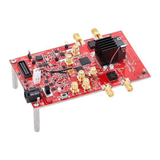
DAC39RF10EVM KEY COMPONENTS
+12V DC
DAC clock input
(LMX CLKP)
OUTAn
OUTAp
DAC39RF10EVM top side with
heat sink installed
Figure 1-1. EVM Orientation
Copyright © 2023 Texas Instruments Incorporated
Table
7-1).
FTDI dongle
connector
FPGA Reference clock
input (LMK CLKP)
OUTBn
OUTBp
Heat Sink for DAC
DAC39RF10EVM bo
DAC39RF10EVM Evaluation Module
FMC+
connector
o m side
¡
1
Advertisement
Table of Contents

Related Manuals for Texas Instruments DAC39RF10EVM


Summary of Contents for Texas Instruments DAC39RF10EVM
-
Page 1: Figure 1-1. Evm Orientation
The DAC39RF10EVM is an evaluation board used to evaluate the DAC39RF10, digital-to-analog converters (DAC) from Texas Instruments.The DAC39RF10 is a family of single and dual channel digital-to-analog converter (DAC) with 16-bit resolution. The devices can be used as single channel or dual channel non-interpolation DACs. - Page 2 With proper hardware selection in the HSDC Pro software, the TSW14J59 board is automatically configured to support a wide range of operating speeds of the DAC39RF10EVM, but the TSW14J59EVM board may not cover the full operating range of the DAC device.
-
Page 3: Table Of Contents
List of Figures Figure 1-1. EVM Orientation................................ Figure 3-1. DAC39RF10EVM Test Setup............................ Figure 3-2. FTDI website to download and install the driver......................6 Figure 3-3. Configuration of DAC39RF10EVM GUI........................Figure 3-4. NCO TAB CONTROLS............................10 Figure 3-5. NCO only JMODE settings for GUI..........................11 Figure 3-6. -
Page 4: Required Equipment
Type C USB cable • FTDI dongle to program the DAC EVM with FTDI. The following equipments are not included in the DAC39RF10EVM kit, but are required for evaluation of this product: • TSW14J59EVM data capture board and related items •... -
Page 5: Setup Procedure
FMC 12V TSW14J59EVM 12V 6A Power Switch Figure 3-1. DAC39RF10EVM Test Setup Note The HSDC Pro software must be installed before connecting the TSW14J59EVM to the PC for the first time. 3.1 Installing the High Speed Data Converter (HSDC) Pro Software 1. -
Page 6: Figure 3-2. Ftdi Website To Download And Install The
4. Run the executable file ( DAC39RF10.exe). Figure 3-2. FTDI website to download and install the driver. 3.3 Connect the DAC39RF10EVM and TSW14J59EVM 1. With the power off, connect the DAC39RF10EVM to the TSW14J59EVM through the FMC+ connector as shown in DAC39RF10EVM Test Setup. -
Page 7: Table 3-1. Powering The Dac39Rf10Evm
GND and the inner portion of the connector is 12 V. Connect the power cable to the TSW14J59EVM power connector. 2. DAC39RF10EVM can be powered with 12-V DC(minimum 2 A) though the connector jack(J1) on the DAC39RF10EVM or it can be powered from the TSW14J59EVM via FMC+ connector. There is a switch(SW1) which can be used to select power from the barrel jack on the DAC EVM or from TSW14J59EVM through FMC+ connector. - Page 8 1. The default option uses the power from FMC+ connector on TSW14J59EVM. For this option, the FMC power switch on TSW14J59EVM should be set to on postion and power switch on the DAC39RF10EVM shoud be set to FMC(defalut). If external power supply is used to power the DAC EVM. Then turn on the 12-V power supply connected to the barrel jack on the DAC EVM and set the power switch postion on DAC39RF10EVM to JACK postion.
-
Page 9: Figure 3-3. Configuration Of Dac39Rf10Evm Gui
Setup Procedure 3.9 Launch the DAC39RF10EVM GUI and Program the DAC EVM The DAC39RF10EVM configuration GUI is installed separately from the HSDC Pro installation and is a stand- alone GUI. Note The max clock rate supported by DAC39RF10EVM is 10240 MHz Figure 3-3. -
Page 10: Figure 3-4. Nco Tab Controls
DAC1. If more than one DUC is routed per DAC, the DUC data into the DAC must be attenuated to prevent the DAC from saturating. DAC39RF10EVM Evaluation Module SBAU395 – APRIL 2023 Submit Document Feedback Copyright © 2023 Texas Instruments Incorporated... -
Page 11: Figure 3-5. Nco Only Jmode Settings For Gui
The NCO only mode can be configured through the GUI by following steps. Figure 3-5. NCO only JMODE settings for GUI. 1. Launch the DAC39RF10EVM GUI. 2. Select the LMX->DACCLK | LMX/LMK->FPGA as the clock source. 3. Enter Clk Freq 10240 MHz. -
Page 12: Figure 3-6. Nco Only Mode Gui Settings
2. Click OK to confirm the serial number of the TSW14J59EVM device. If multiple TSWxxxxx boards are connected, select the model and serial number for the one connected to the DAC39RF10EVM. 3. For Device select DAC from drop down menu. -
Page 13: Figure 3-7. Launching Hsdcpro And Setup
If the user configures the EVM with options other than the default register values, different instructions may be required for selecting the device in HSDC Pro. See Section 7 for more details. SBAU395 – APRIL 2023 DAC39RF10EVM Evaluation Module Submit Document Feedback Copyright © 2023 Texas Instruments Incorporated... -
Page 14: Figure 3-8. Hsdcpro Setup
DAC39RF10EVM GUI. 7. For DAC Option dropdown select the "Offset Bin" option.( The DAC39RF10EVM gui always defaults to offset binary). 8. Navigate to lower left side of the HSDCpro GUI to I/Q Multitone Generator section. For # of tones enter 1, for Tone Center enter 1G( 1 GHz or desired frequency), # Samples can be left 65536. -
Page 15: Figure 3-9. Hsdcpro Generating The Tone And Sending It To The Dac
Setup Procedure Figure 3-9. HSDCpro Generating the Tone and Sending it to the DAC. Figure 3-10. DAC Output Displayed on Spectrum Analyzer SBAU395 – APRIL 2023 DAC39RF10EVM Evaluation Module Submit Document Feedback Copyright © 2023 Texas Instruments Incorporated... -
Page 16: Device Configuration
Perform a generic read or write command to the device shown in the Block drop-down box using the read or write register buttons address and write data information DAC39RF10EVM Evaluation Module SBAU395 – APRIL 2023 Submit Document Feedback Copyright © 2023 Texas Instruments Incorporated... -
Page 17: Figure 4-1. Register Map Tab
Device Configuration Figure 4-1. Register Map Tab SBAU395 – APRIL 2023 DAC39RF10EVM Evaluation Module Submit Document Feedback Copyright © 2023 Texas Instruments Incorporated... -
Page 18: Troubleshooting The Dac39Rf10Evm
Check that the spectrum analyzer is set to proper settings. Output power looks low • SMA connector is properly connect to the DAC output and Spectrum analyzer. DAC39RF10EVM Evaluation Module SBAU395 – APRIL 2023 Submit Document Feedback Copyright © 2023 Texas Instruments Incorporated... -
Page 19: References
LMX1204 data sheet • FTDI USB to Serial Driver Installation Manual (www.ftdichip.com/Support/Documents/InstallGuides.htm) 6.2 TSW14J59EVM Operation Refer to the TSW14J59EVM user guide for configuration and status information. SBAU395 – APRIL 2023 DAC39RF10EVM Evaluation Module Submit Document Feedback Copyright © 2023 Texas Instruments Incorporated... -
Page 20: Appendix
This appendix provides settings for optional ADC device configuration in HSDC Pro. 7.1 Customizing the EVM for Optional Clocking Support The DAC39RF10EVM can be clocked using 3 different methods: LMX->DACCLK | LMX/LMK-> FPGA option, EXT->DACCLK | LMX/LMK-> FPGA option and EXT->DACCLK | LMK-> FPGA option. -
Page 21: Figure 7-2. Ext->Dacclk | Lmx/Lmk-> Fpga Clocking System Block
7.1.2 EXT->DACCLK | LMX/LMK-> FPGA Clocking Option The DAC39RF10EVM can be configured to use EXT->DACCLK | LMX/LMK-> FPGA Clocking option. Similar to above use case The user provide a single high frequency (10-15 dBm) signal to an SMA labeled LMX CLKp. -
Page 22: Figure 7-3. External Reference Clocking System Block Diagram
7.1.3 EXT->DACCLK | LMK-> FPGA Clocking Option The DAC39RF10EVM can be configured to use EXT->DACCLK | LMK-> FPGA Clocking option. In this use case, the user provide a two clock signal. A high frequency(10-15dBm) signal to an SMA labeled LMX CLKp. -
Page 23: Table 7-1. Dac39Rf10Evm Signal Routing
Appendix 7.2 Signal Routing Table 7-1 provides the signal routing details for the DAC39RF10EVM. Table 7-1. DAC39RF10EVM Signal Routing JESD204C FMC(+) Pi FMC(+) Signal Names Inputs Lane0 A38,A39 DP5_C2M_INV Lane1 B36,B37 DP6_C2M_INV Lane2 B32,B33 DP7_C2M_INV Lane3 A34,A35 DP4_C2M_INV Lane4... -
Page 24: Figure 7-4. Analog Outut Path
Appendix www.ti.com Figure 7-4. Analog Outut Path DAC39RF10EVM Evaluation Module SBAU395 – APRIL 2023 Submit Document Feedback Copyright © 2023 Texas Instruments Incorporated... -
Page 25: Figure 7-5. 3 Db Attenuation Pad
A 3 dB attenuation pad is added between the inputs and the ADC. The 3 dB pad helps with the flatness of the frequency response. Figure 7-5. 3 dB attenuation pad SBAU395 – APRIL 2023 DAC39RF10EVM Evaluation Module Submit Document Feedback Copyright © 2023 Texas Instruments Incorporated... -
Page 26: Table 7-3. Jumper Settings
FMC+ connector are controlling the devices on the EVM(This feature will be supported on next rev of the board). Table 7-4. LEDs Label Function 12 V power indicator DAC39RF10EVM Evaluation Module SBAU395 – APRIL 2023 Submit Document Feedback Copyright © 2023 Texas Instruments Incorporated... - Page 27 STANDARD TERMS FOR EVALUATION MODULES Delivery: TI delivers TI evaluation boards, kits, or modules, including any accompanying demonstration software, components, and/or documentation which may be provided together or separately (collectively, an “EVM” or “EVMs”) to the User (“User”) in accordance with the terms set forth herein.
- Page 28 www.ti.com Regulatory Notices: 3.1 United States 3.1.1 Notice applicable to EVMs not FCC-Approved: FCC NOTICE: This kit is designed to allow product developers to evaluate electronic components, circuitry, or software associated with the kit to determine whether to incorporate such items in a finished product and software developers to write software applications for use with the end product.
- Page 29 www.ti.com Concernant les EVMs avec antennes détachables Conformément à la réglementation d'Industrie Canada, le présent émetteur radio peut fonctionner avec une antenne d'un type et d'un gain maximal (ou inférieur) approuvé pour l'émetteur par Industrie Canada. Dans le but de réduire les risques de brouillage radioélectrique à...
- Page 30 www.ti.com EVM Use Restrictions and Warnings: 4.1 EVMS ARE NOT FOR USE IN FUNCTIONAL SAFETY AND/OR SAFETY CRITICAL EVALUATIONS, INCLUDING BUT NOT LIMITED TO EVALUATIONS OF LIFE SUPPORT APPLICATIONS. 4.2 User must read and apply the user guide and other available documentation provided by TI regarding the EVM prior to handling or using the EVM, including without limitation any warning or restriction notices.
- Page 31 Notwithstanding the foregoing, any judgment may be enforced in any United States or foreign court, and TI may seek injunctive relief in any United States or foreign court. Mailing Address: Texas Instruments, Post Office Box 655303, Dallas, Texas 75265 Copyright © 2023, Texas Instruments Incorporated...
- Page 32 TI products. TI’s provision of these resources does not expand or otherwise alter TI’s applicable warranties or warranty disclaimers for TI products. TI objects to and rejects any additional or different terms you may have proposed. IMPORTANT NOTICE Mailing Address: Texas Instruments, Post Office Box 655303, Dallas, Texas 75265 Copyright © 2023, Texas Instruments Incorporated...
Need help?
Do you have a question about the DAC39RF10EVM and is the answer not in the manual?
Questions and answers