
Related Manuals for Quectel SC200R Series


Summary of Contents for Quectel SC200R Series
- Page 1 SC200R&SC262R Series Hardware Design Smart Module Series Version: 1.2 Date: 2022-05-23 Status: Released...
- Page 2 To the maximum extent permitted by law, Quectel excludes all liability for any loss or damage suffered in connection with the use of the functions and features under development, regardless of whether such loss or damage may have been foreseeable.
-
Page 3: Safety Information
Manufacturers of the cellular terminal should send the following safety information to users and operating personnel, and incorporate these guidelines into all manuals supplied with the product. If not so, Quectel assumes no liability for customers’ failure to comply with these precautions. -
Page 4: About The Document
Smart Module Series About the Document Revision History Version Date Author Description 2019-12-30 Arsene TONG Initial 1. Updated SC200R-EM frequency bands (Chapter 2.1/6.1): Added B4 in LTE-FDD Deleted B39 in LTE-TDD Added B4 in WCDMA 2. Added Galileo supported GNSS (Chapter 2.1/2.2/5/6.3). - Page 5 Smart Module Series SC200R-CE/-EM/-NA. 3. Chapter 7.5: Added output power SC200R-EM. 4. Chapter 7.6: Updated RF receiving sensitivity of SC200R-CE/-EM/-NA. 5. Chapter 9.1: Updated notes for the storage conditions. 6. Chapter 9.2: Updated the recommended reflow soldering thermal profile parameters. 2022-5-23 Winston 1.
-
Page 6: Table Of Contents
Smart Module Series Contents Safety Information ............................2 About the Document ........................... 3 Contents ............................... 5 Table Index ..............................8 Figure Index ............................... 10 Introduction ............................12 1.1. Special Mark ..........................16 Product Concept ..........................17 2.1. General Description ......................... 17 2.2. - Page 7 Smart Module Series 3.22. Audio Interfaces ........................70 3.22.1. Reference Circuit Design for Microphone Interfaces ............. 71 3.22.2. Reference Circuit Design for Earpiece Interface ............72 3.22.3. Reference Circuit Design for Headset Interface ............73 3.22.4. Reference Circuit Design for Loudspeaker Interface............. 73 3.22.5.
- Page 8 Smart Module Series 9.2. Manufacturing and Soldering ....................116 9.3. Packaging ..........................118 10 Appendix References ........................120 SC200R&SC262R_Series_Hardware_Design 7 / 124...
- Page 9 Smart Module Series Table Index Table 1: Special Mark ..........................16 Table 2: SC200R-CE Frequency Bands ....................17 Table 3: SC200R-EM Frequency Bands ....................18 Table 4: SC200R-NA Frequency Bands..................... 18 Table 5: SC200R-JP* Frequency Bands ....................19 Table 6: SC200R-WF Frequency Bands ....................19 Table 7: Key Features ..........................
- Page 10 Smart Module Series Table 42: GNSS Frequency ........................86 Table 43: Antenna Requirements ....................... 90 Table 44: Absolute Maximum Ratings ......................93 Table 45: Power Supply Ratings ........................ 93 Table 46: Operating and Storage Temperatures ..................94 Table 47: SC200R-CE Current Consumption .................... 94 Table 48: SC200R-EM Current Consumption ....................
- Page 11 Smart Module Series Figure Index Figure 1: Functional Diagram ........................23 Figure 2: Pin Assignment (Top View) ......................25 Figure 3: Voltage Drop Sample ........................40 Figure 4: Star Structure of the Power Supply .................... 41 Figure 5: Reference Circuit of Power Supply ..................... 41 Figure 6: Turn on the Module Using Driving Circuit ...................
- Page 12 Smart Module Series Figure 42: Bottom Dimensions (Bottom View) ..................112 Figure 43: Recommended Footprint (Top View) ..................113 Figure 44: Top and Bottom Views of the Module ..................114 Figure 45: Recommended Reflow Soldering Thermal Profile ..............117 Figure 46: Tape Dimensions (Unit: mm) ....................118 Figure 47: Reel Dimensions (Unit: mm) ....................
-
Page 13: Introduction
Smart Module Series Introduction This document, describing SC200R series module and its air and hardware interfaces connected to your applications, informs you of the interface specifications, electrical and mechanical details, as well as other related information of the module. With the application notes and user guides provided separately, you can easily use the module to design and set up mobile applications. - Page 14 Important Note notice that any deviation(s) from the defined parameters of the antenna trace, as described by the instructions, require that the host product manufacturer must notify to Quectel Wireless Solutions Co., Ltd that they wish to change the antenna trace design. In this case, a Class II permissive change application is required to be filed by the USI, or the host manufacturer can take responsibility through the change in FCC ID (new application) procedure followed by a Class II permissive change application.
- Page 15 Smart Module Series Le pré sent appareil est conforme aux CNR d’ ISED applicables aux appareils radio exempts de licence. L’exploitation est autorisé e aux deux conditions suivantes : (1) le dispositif ne doit pas produire de brouillage pré judiciable, et (2) ce dispositif doit accepter tout brouillage reç u, y compris un brouillage susceptible de provoquer un fonctionnement indé...
- Page 16 Smart Module Series l'inté grateur OEM sera chargé de ré é valuer le produit final (y compris l'é metteur) et l'obtention d'une autorisation distincte au Canada. End Product Labeling This transmitter module is authorized only for use in device where the antenna may be installed such that 20 cm may be maintained between the antenna and users.
-
Page 17: Special Mark
Smart Module Series d’inclinaison nécessaires pour rester conforme à l’exigence de la p.i.r.e. applicable au masque d’élévation, énoncé e à la section 6.2.2.3, doivent être clairement indiqués. i. for devices with detachable antenna(s), the maximum antenna gain permitted for devices in the bands 5250-5350 MHz and 5470-5725 MHz shall be such that the equipment still complies with the e.i.r.p. -
Page 18: Product Concept
⚫ Provides multiple audio and video input/output interfaces as well as abundant GPIO interfaces. SC200R series module is available in below variants: SC200R-CE, SC200R-EM, SC200R-NA, SC200R-JP*, SC200R-WF, SC262RWF. The following tables show the supported frequency bands and network standards of SC200R series modules. - Page 19 Smart Module Series GPS: 1575.42 ± 1.023 MHz GLONASS: 1597.5–1605.8 MHz GNSS BeiDou: 1561.098 ± 2.046 MHz Galileo: 1575.42 ± 1.023 MHz Table 3: SC200R-EM Frequency Bands Mode Frequency LTE-FDD B1/B2/B3/B4/B5/B7/B8/B20/B28 LTE-TDD B38/B40/B41 WCDMA B1/B2/B4/B5/B8 850/900/1800/1900 MHz 2412–2472 MHz Wi-Fi 802.11a/b/g/n 5180–5825 MHz Bluetooth 4.2 LE 2402–2480 MHz...
- Page 20 Smart Module Series Table 5: SC200R-JP* Frequency Bands Mode Frequency LTE-FDD B1/B3/B5/B8/B11/B18/B19/B21/B26/B28 LTE-TDD WCDMA B1/B6/B8/B19 2402–2482 MHz Wi-Fi 802.11a/b/g/n 5180–5825 MHz Bluetooth 4.2 LE 2402–2480 MHz GPS: 1575.42 ± 1.023 MHz GLONASS: 1597.5–1605.8 MHz GNSS BeiDou: 1561.098 ± 2.046 MHz Galileo: 1575.42 ±...
-
Page 21: Key Features
CPE, wireless POS, smart metering, router, data card, automotive, smart phone, digital signage, alarm panel, security and industry PDA, etc. 2.2. Key Features The following table describes the detailed features of SC200R series module. Table 7: Key Features Feature Details ⚫... - Page 22 Smart Module Series Supports 3GPP R10 Cat 4 FDD and TDD Supports 1.4/3/5/10/15/20 MHz RF bandwidth LTE Features ⚫ FDD: Max. 150 Mbps (DL)/Max. 50 Mbps (UL) ⚫ TDD: Max. 130 Mbps (DL)/Max. 30 Mbps (UL) Supports 3GPP R9 DC-HSDPA/DC-HSUPA/HSPA+/HSDPA/HSUPA/WCDMA Supports 16-QAM, 64-QAM and QPSK modulations ⚫...
- Page 23 Smart Module Series Audio inputs: ⚫ Three single-ended microphone inputs Audio outputs: Audio Interfaces ⚫ Class AB stereo headphone output ⚫ Class AB earpiece differential output ⚫ Class D speaker differential amplifier output ⚫ EVRC, EVRC-B, EVRC-WB; ⚫ G.711, G.729A, and G.729AB; Audio Codec ⚫...
-
Page 24: Functional Diagram
NOTES SC200R-WF/SC262R-WF does not support GNSS. Within the operating temperature range, the module is 3GPP compliant. 2.3. Functional Diagram The following figure shows a block diagram of SC200R series module and illustrates the major functional parts. ⚫ Power management ⚫... -
Page 25: Application Interfaces
Smart Module Series Application Interfaces 3.1. General Description SC200R is a series of SMD type modules with 146 LCC pins and 128 LGA pins. The following chapters provide the detailed description of pins/interfaces listed below. ⚫ Power supply ⚫ VRTC interface ⚫... -
Page 26: Pin Assignment
Smart Module Series 3.2. Pin Assignment The following figure shows the pin assignment of SC200R series module. GPIO_42 VBAT_BB VBAT_BB GPIO_44 GPIO_63 MIC1_P GPIO_43 MIC_GND GPIO_66 MIC2_P GPIO_87 GPIO_94 GPIO_95 EAR_P GPIO_13 EAR_N GPIO_12 SPK_P GPIO_59 SPK_N GPIO_48 GPIO_45 USB_DM... -
Page 27: Pin Description
Smart Module Series 3.3. Pin Description Table 8: I/O Parameters Definition Type Description Analog input Analog output Analog input/output Digital input Digital output Digital input/output Open drain Power input Power output Power input/output The following table shows the pin definition and electrical characteristics of the module. Table 9: Pin Description Power Supply Pin Name... - Page 28 Smart Module Series Power supply for external GPIO’s 1.8 V output Vnom = 1.8 V LDO5_1V8 power supply max = 20 mA pull-up and level shift circuits. Power supply for sensors, cameras, and I2C pull-up circuit. If it is used, connect 1.8 V output Vnom = 1.8 V LDO6_1V8...
- Page 29 Smart Module Series 3, 7, 12, 15, 27, 51, 62, 69, 76, 78, 85, 86, 88, 89, 120, 122, 130, 132, 135, 140, 143, 144, 149, 162, 171, 172, 176, 187–191, 202–204, 206–224, 226–231, 233–238, 240, 241, 243–245, 247, 248, 250, 251, 255, 256, 258, 259, 261, 266, 268, 269, 271–274 Audio Interfaces Pin Name...
- Page 30 Smart Module Series Charging power input; USB 5 V Vmax = 6.2 V 141, USB_VBUS power input; Vmin = 4.35 V USB/adaptor Vnom = 5.0 V insertion detection USB 2.0 USB 2.0 standard USB_DM differential data (-) compliant. 90 Ω differential USB 2.0 USB_DP impedance.
- Page 31 Smart Module Series max = 55 mA For 1.8 V (U)SIM: Vmax = 1.85 V Either 1.8 V or (U)SIM2 card USIM2_VDD Vmin = 1.75 V 2.95 V (U)SIM card power supply is supported. For 2.95 V (U)SIM: Vmax = 3.1 V Vmin = 2.8 V Active low.
- Page 32 Smart Module Series max = 0.45 V UART5_TXD UART5 transmit min = 1.35 V max = 0.63 V UART5_RXD UART5 receive min = 1.17 V UART5 clear to max = 0.63 V UART5_CTS send min = 1.17 V UART5 request to max = 0.45 V UART5_RTS send...
- Page 33 Smart Module Series 2.95 V SD card: max = 0.73 V SD_DATA3 SDIO data bit 3 min = 1.84 V max = 0.37 V min = 2.2 V SD card hot-plug max = 0.63 V SD_DET Active low. detect min = 1.17 V Touch Panel Interface Pin Name Pin No.
- Page 34 Smart Module Series LCD MIPI data 2 DSI_LN2_P LCD MIPI data 3 DSI_LN3_N LCD MIPI data 3 DSI_LN3_P Camera Interfaces Pin Name Pin No. Description DC Characteristics Comment Camera MIPI CSI1_CLK_N clock (-) Camera MIPI clock CSI1_CLK_P Camera MIPI CSI1_LN0_N data 0 (-) Camera MIPI CSI1_LN0_P...
- Page 35 Smart Module Series Camera MIPI CSI0_LN2_N data 2 (-) Camera MIPI CSI0_LN2_P data 2 (+) Camera MIPI CSI0_LN3_N data 3 (-) Camera MIPI CSI0_LN3_P data 3 (+) CAM0_MCLK Clock of camera CAM1_MCLK Clock of camera CAM0_RST Reset of camera max = 0.45 V 1.8 V power Power down of min = 1.35 V...
- Page 36 Smart Module Series If it is not used, keep it open. max = 0.63 V Cannot be VOL_UP Volume up min = 1.17 V externally pulled up. 1.8 V power domain. If it is not used, keep it open. max = 0.63 V Cannot be VOL_DOWN Volume down...
- Page 37 Smart Module Series If you use an internal charging chip, keep this pin open. CHG_SEL Charging select If you use an external charging chip, connect it to GND. ADC Interface Pin Name Pin No. Description DC Characteristics Comment General-purpose The maximum input ADC interface voltage is 1.7 V.
- Page 38 Smart Module Series General-purpose GPIO_13 input/output General-purpose GPIO_95 input/output General-purpose GPIO_94 input/output General-purpose GPIO_87 input/output General-purpose GPIO_66 input/output General-purpose GPIO_43 input/output General-purpose GPIO_63 input/output General-purpose GPIO_44 input/output General-purpose GPIO_42 input/output General-purpose GPIO_93 input/output General-purpose GPIO_46 input/output General-purpose GPIO_89 input/output General-purpose GPIO_23 input/output General-purpose...
- Page 39 Smart Module Series General-purpose GPIO_34 input/output General-purpose GPIO_90 input/output General-purpose GPIO_39 input/output General-purpose GPIO_86 input/output Cannot be pulled up General-purpose during power-on. GPIO_88 input/output 1.8 V power domain. General-purpose GPIO_85 input/output 1.8 V power domain. General-purpose GPIO_61 input/output GNSS LNA Enable Interface Pin Name Pin No.
- Page 40 Smart Module Series Pin Name Pin No. Description DC Characteristics Comment Vibration motor Connect it to the = 1.2–3.1 V VIB_DRV_N driver output negative pole of the max = 175 mA control motor. Indication Interface Pin Name Pin No. Description DC Characteristics Comment Indicates the...
-
Page 41: Power Supply
3.4. Power Supply 3.4.1. Power Supply Pins SC200R series module provides two VBAT_RF pins and two VBAT_BB pins for connection with the external power supply. The VBAT_RF pins are used for the RF part of the module and the VBAT_BB pins are used for the baseband part of the module. -
Page 42: Reference Design For Power Supply
The power design for the module is very important, as the performance of the module largely depends on the power source. The power supply of SC200R series module should be able to provide sufficient current of at least 3 A. If the voltage drop between the input and output is not too high, it is suggested to use an LDO to supply power for the module. -
Page 43: Turn On And Off Scenarios
Smart Module Series NOTES It is recommended to switch off the power supply when the module is in abnormal state, and then switch on the power to restart the module. The module supports battery charging by default. If the above power supply design is adopted, make sure the charging function is disabled by software, or connect VBAT to a Schottky diode in series to avoid the reverse current to the power supply chip. - Page 44 Smart Module Series The other way to control PWRKEY is by using a button directly. You must place a TVS component nearby the button for ESD protection. A reference circuit is shown in the following figure. PWRKEY Close to S1 Figure 6: Turn on the Module Using Keystroke The turning-on scenario is illustrated in the following figure.
-
Page 45: Turn Off The Module
Smart Module Series NOTES 1. When the module is powered on for the first time, its timing of turning on may be different from that shown above. 2. Make sure that VBAT is stable before pulling down PWRKEY. It is recommended to wait until VBAT to be stable at 3.8 V for at least 30 ms before pulling down PWRKEY. -
Page 46: Power Output
VRTC is 2.0–3.25 V and the recommended typical value is 3.0 V. 3.7. Power Output SC200R series module supports output of regulated voltages for peripheral circuits. During application, it is recommended to connect a 33 pF and a 10 pF capacitor in parallel in the circuit to suppress high-frequency noise. -
Page 47: Battery Charging And Management
LDO for power supply. 3.8. Battery Charging and Management SC200R series module supports battery charging. The battery charger IC in the module supports trickle charging, constant current charging and constant voltage charging modes, which optimize the charging procedure for Li-ion batteries. - Page 48 If you use an external charging chip, connect it to GND. SC200R series module supports battery temperature detection in the condition that the battery integrates a thermistor (47 kΩ 1 % NTC thermistor with a B-constant of 4050 K by default) and the thermistor is connected to BAT_THERM pin.
-
Page 49: Usb Interface
Smart Module Series 3.9. USB Interface SC200R series module provides one integrated Universal Serial Bus (USB) interface which complies with USB 2.0 specification and supports high-speed (480 Mbps) and full-speed (12 Mbps) modes. The USB interface supports USB OTG and is used for AT command communication, data transmission, software debugging and firmware upgrade. - Page 50 Smart Module Series VBAT VOUT 1.0 μH VOUT 10 μF 22 μF/ 10 V GPIO VBAT USB_VBUS VUSB USB_DM USB_DM USB_DP USB_DP USB_ID USB_ID Module 100 nF Figure 12: USB Interface Reference Design (OTG Supported) In order to ensure USB performance, comply with the following principles when designing the USB interface.
-
Page 51: Uart Interfaces
Smart Module Series 3.10. UART Interfaces SC200R series module provides three UART interfaces and supports up to 4 Mbps: ⚫ UART5: 4-wire UART interface, and hardware flow control is supported ⚫ UART2 (debug UART): 2-wire UART interface, used for debugging by default ⚫... -
Page 52: U)Sim Interfaces
UART2 and UART1 are similar to UART5. For the reference design, refer to that of UART5. 3.11. (U)SIM Interfaces SC200R series module provides two (U)SIM interfaces that meet ETSI and IMT-2000 requirements. Dual SIM Dual Standby is supported by default. Either 1.8 V or 2.95 V (U)SIM card is supported, and the (U)SIM card is powered by the internal power supply of the module. - Page 53 (U)SIM1 card power supply card is supported. SC200R series module supports (U)SIM card hot-plug via the USIM_DET pin. (This function is disabled by default via software. To enable it, contact Quectel Technical Supports to change the software configuration.) A reference circuit for (U)SIM interface with an 8-pin (U)SIM card connector is shown below.
- Page 54 Smart Module Series If you do not need to use USIM_DET, keep this pin open. The following is a reference circuit for (U)SIM interface with a 6-pin (U)SIM card connector. USIM_ VDD USIM_VDD (U)SIM card connector 100 nF USIM_VDD USIM_RST USIM_CLK Module USIM_DATA...
-
Page 55: Sd Card Interface
Smart Module Series 3.12. SD Card Interface SD Card interface of SC200R series module supports SD 3.0 protocol. The pin definition of SD card interface is shown below. Table 16: Pin Definition of SD Card Interface Pin Name Pin No. - Page 56 Smart Module Series SD_LDO11 is the power supply for the SD card and can provide up to 800 mA output current. Due to the high output current, it is recommended that the trace width should be at least 0.8 mm. In order to ensure stability of output current, add a 4.7 μF and a 33 pF capacitor in parallel near the SD card connector.
-
Page 57: Gpio Interfaces
Smart Module Series 3.13. GPIO Interfaces SC200R series module has abundant GPIO interfaces with a power domain of 1.8 V. The pin definition is listed below. Table 18: Pin Definition of GPIO Interfaces Pin Name Pin No. GPIO No. Default State... - Page 58 Smart Module Series GPIO_59 GPIO_59 B-PD:nppukp Wakeup GPIO_61 GPIO_61 B-PD:nppukp Wakeup GPIO_62 GPIO_62 B-PD:nppukp Wakeup GPIO_63 GPIO_63 B-PD:nppukp Wakeup GPIO_66 GPIO_66 B-PD:nppukp GPIO_85 GPIO_85 B-PD:nppukp GPIO_86 GPIO_86 B-PD:nppukp Wakeup GPIO_87 GPIO_87 B-PD:nppukp GPIO_88 GPIO_88 B-PD:nppukp GPIO_89 GPIO_89 B-PD:nppukp GPIO_90 GPIO_90 B-PD:nppukp Wakeup GPIO_93...
- Page 59 Smart Module Series CAM0_RST GPIO_128 B-PD:nppukp Wakeup CAM0_PWDN GPIO_126 B-PD:nppukp Wakeup CAM1_RST GPIO_129 B-PD:nppukp CAM1_PWDN GPIO_125 B-PD:nppukp CAM2_MCLK GPIO_27 B-PD:nppukp CAM2_RST GPIO_38 B-PD:nppukp Wakeup CAM2_PWDN GPIO_41 B-PD:nppukp Wakeup VOL_UP GPIO_91 B-PD:nppukp Wakeup VOL_DOWN GPIO_50 B-PD:nppukp Wakeup UART5_TXD GPIO_16 B-PD:nppukp UART5_RXD GPIO_17 B-PD:nppukp Wakeup...
-
Page 60: I2C Interfaces
Smart Module Series 3.14. I2C Interfaces SC200R series module provides four I2C interfaces. All I2C interfaces are open drain signals and therefore you must pull them up externally. The reference power domain is 1.8 V. The SENSOR_I2C interface only supports sensors of ADSP architecture. CAM_I2C and DCAM_I2C signals are controlled by Linux Kernel code and support connection with devices related to video output. -
Page 61: Adc Interface
Can be multiplexed into SPI7_MISO 3.16. ADC Interface SC200R series module supports one analog-to-digital converter (ADC) interface. The ADC interface supports resolution of up to 15 bits. The pin definition is shown below. Table 21: Pin Definition of ADC Interface Pin Name Pin No. -
Page 62: Lcm Interface
3.18. LCM Interface SC200R series module provides one LCM interface, which is MIPI_DSI standard compliant. The interface supports high-speed differential data transmission and supports HD+ display (1440 × 720 @ 60 fps). The pin definition of the LCM interface is shown below. - Page 63 Smart Module Series DSI_LN0_N LCD MIPI data 0 (-) DSI_LN0_P LCD MIPI data 0 (+) DSI_LN1_N LCD MIPI data 1 (-) DSI_LN1_P LCD MIPI data 1 (+) DSI_LN2_N LCD MIPI data 2 (-) DSI_LN2_P LCD MIPI data 2 (+) DSI_LN3_N LCD MIPI data 3 (-) DSI_LN3_P LCD MIPI data 3 (+)
-
Page 64: Touch Panel Interface
Figure 20: Reference Design for External Backlight Driving Circuit 3.19. Touch Panel Interface SC200R series module provides one I2C interface for connection with Touch Panel (TP), and also provides the corresponding power supply and interrupt pins. The definitions of TP interface pins are illustrated below. - Page 65 Smart Module Series TP_INT TP interrupt 1.8 V voltage domain. 1.8 V voltage domain . TP_RST TP reset Active low. Externally pull them up to 1.8 V. TP_I2C_SCL TP I2C clock Can be used for other I2C TP_I2C_SDA TP I2C data devices.
-
Page 66: Camera Interfaces
Smart Module Series 3.20. Camera Interfaces Based on MIPI_CSI standard, SC200R series module supports two cameras (4-lane + 4-lane) or three cameras (4-lane + 2-lane + 1-lane), and the maximum pixel of the camera can be up to 13 MP. The video and photo quality is determined by various factors such as the camera sensor, camera lens quality, etc. - Page 67 Smart Module Series CSI0_LN2_N Camera MIPI data 2 (-) CSI0_LN2_P Camera MIPI data 2 (+) CSI0_LN3_N Camera MIPI data 3 (-) CSI0_LN3_P Camera MIPI data 3 (+) CAM0_MCLK Clock of camera CAM1_MCLK Clock of camera CAM0_RST Reset of camera 1.8 V power domain. CAM0_PWDN Power down of camera CAM1_RST...
- Page 68 Smart Module Series The following is a reference circuit design for 3-camera applications. 1 μF AF_VDD VBAT GPIO LDO17_2V85 1 μF AVDD VBAT GPIO DVDD DOVDD CAM2_ RST LDO6_1V8 CAM2_PWDN CAM2_MCLK DCAM_I2C_SDA DCAM_I2C_SCL CSI0_LN3_P CSI0_LN3_N CSI0_LN2_P CSI0_LN2_N CSI0_LN1_P CSI0_LN1_N CSI0_LN0_P CSI0_LN0_N CSI0_CLK_P 1 μF...
-
Page 69: Design Considerations
Smart Module Series NOTE In 3-camera applications, CSI1_LN3_P and CSI1_LN3_N are used as CLK_P and CLK_N of camera1, CSI1_LN2_P and CSI1_LN2_N are used as the LN_P and LN_N of camera1. 3.20.1. Design Considerations ⚫ Special attention should be paid to the pin definition of LCM/camera connectors. Make sure the module and the connectors are correctly connected. - Page 70 Smart Module Series DSI_LN3_P 12.35 CSI1_CLK_N 18.10 -0.05 CSI1_CLK_P 18.05 CSI1_LN0_N 18.05 0.05 CSI1_LN0_P 18.10 CSI1_LN1_N 18.15 0.05 CSI1_LN1_P 18.20 CSI1_LN3_N 18.10 0.10 CSI1_LN3_P 18.20 CSI1_LN2_N 18.05 0.05 CSI1_LN2_P 18.10 CSI0_CLK_N 22.60 -0.05 CSI0_CLK_P 22.55 CSI0_LN0_N 22.55 -0.05 CSI0_LN0_P 22.50 CSI0_LN1_N 20.25 0.05...
-
Page 71: Sensor Interfaces
Smart Module Series 3.21. Sensor Interfaces SC200R series module supports communication with sensors via I2C interfaces, and it supports ALS/PS, compass, accelerometer, gyroscope, etc. Table 27: Pin Definition of Sensor Interfaces Pin Name Pin No. Description Comment Dedicated for external sensors. -
Page 72: Reference Circuit Design For Microphone Interfaces
Smart Module Series MIC3_P Microphone input for channel 2 (+) MIC_BIAS1 Microphone bias voltage 1 = 1.6–2.85 V EAR_P Earpiece output (+) EAR_N Earpiece output (-) SPK_P Speaker output (+) SPK_N Speaker output (-) HPH_R Headphone right channel output HPH_REF Headphone reference ground HPH_L Headphone left channel output... -
Page 73: Reference Circuit Design For Earpiece Interface
Smart Module Series 100nF MIC_BIAS1 MIC_ GND 33 pF MIC3_P MEMS MIC Module 33 pF Figure 24: Reference Circuit Design for MEMS Microphone Interface 3.22.2. Reference Circuit Design for Earpiece Interface 33 pF EAR_P 33 pF EAR_N 33 pF Module Figure 25: Reference Circuit Design for Earpiece Interface SC200R&SC262R_Series_Hardware_Design 72 / 124... -
Page 74: Reference Circuit Design For Headset Interface
Smart Module Series 3.22.3. Reference Circuit Design for Headset Interface MIC_GND MIC2_P HPH_L HS_DET HPH_R HPH_REF D1 D2 D3 D4 33 pF 33 pF 33 pF Module Figure 26: Reference Circuit Design for Headphone Interface 3.22.4. Reference Circuit Design for Loudspeaker Interface SPK_P EARP SPK_N... -
Page 75: Emergency Download Interface
Smart Module Series technique. Therefore, you should consult the capacitor vendors to choose the most suitable capacitor to filter out the high-frequency noises. The severity of RF interference in the voice channel during GSM transmitting largely depends on the application design. In some cases, EGSM900 TDD noise is more severe; while in other cases, DCS1800 TDD noise is more obvious. -
Page 76: Wi-Fi And Bluetooth
PCB antenna, sucker antenna, and ceramic antenna to the module via the interface to achieve Wi-Fi and Bluetooth functions. 4.1. Wi-Fi Overview SC200R series module supports 2.4 GHz and 5 GHz dual-band WLAN based on IEEE 802.11a/b/g/n standard protocols. The maximum data rate is up to 150 Mbps. The features are as below: ⚫... - Page 77 Smart Module Series 802.11n HT20 MCS7 13 dBm ± 2.5 dB 802.11n HT40 MCS0 14 dBm ± 2.5 dB 802.11n HT40 MCS7 13 dBm ± 2.5 dB 802.11a 6 Mbps 15 dBm ± 2.5 dB 802.11a 54 Mbps 13 dBm ± 2.5 dB 802.11n HT20 MCS0 14 dBm ±...
-
Page 78: Bluetooth Overview
IEEE Std 802.11a, IEEE Std 802.11b, IEEE Std 802.11g: IEEE 802.11-2007 WLAN MAC and PHY, June 2007 4.2. Bluetooth Overview SC200R series module supports Bluetooth 4.2 (BR/EDR + BLE) specification, as well as GFSK, 8-DPSK, π/4-DQPSK modulation modes. ⚫ Maximally supports up to 7 wireless connections. -
Page 79: Bluetooth Performance
Smart Module Series 4.2.1. Bluetooth Performance The following table lists the Bluetooth transmitting and receiving performance of SC200R series module. Table 32: Bluetooth Transmitting and Receiving Performance Transmitter Performance Packet Types 2-DH5 3-DH5 Transmitting Power 10.0 10.0 Receiver Performance Packet Types... -
Page 80: Gnss
Smart Module Series GNSS SC200R series module integrates a IZat™ GNSS engine (GEN 8C) which supports multiple positioning and navigation systems including GPS, GLONASS, Galileo and BeiDou. With an embedded LNA, the module provides greatly improved positioning accuracy. 5.1. GNSS Performance The following table lists the GNSS performance of the module in conduction mode. -
Page 81: Gnss Rf Design Guidelines
Smart Module Series 5.2. GNSS RF Design Guidelines Bad design of antenna and layout may cause reduced GNSS receiving sensitivity, longer GNSS positioning time, or reduced positioning accuracy. In order to avoid this, follow the reference design rules as below: ⚫... -
Page 82: Antenna Interfaces
Smart Module Series Antenna Interfaces SC200R series module provides four antenna interfaces for the main antenna, Rx-diversity antenna, Wi-Fi/Bluetooth antenna and GNSS antenna respectively. The impedance of the antenna ports should be controlled to 50 Ω. 6.1. Main/Rx-diversity Antenna Interfaces The pin definition of main/Rx-diversity antenna interfaces is shown below. - Page 83 Smart Module Series LTE-FDD B1 2110–2170 1920–1980 LTE-FDD B3 1805–1880 1710–1785 LTE-FDD B5 869–894 824–849 LTE-FDD B8 925–960 880–915 LTE-TDD B34 2010–2025 2010–2025 LTE-TDD B38 2570–2620 2570–2620 LTE-TDD B39 1880–1920 1880–1920 LTE-TDD B40 2300–2400 2300–2400 LTE-TDD B41 2535–2675 2535–2675 Table 36: SC200R-EM Operating Frequencies 3GPP Band Receive Transmit...
- Page 84 Smart Module Series LTE-FDD B5 869–894 824–849 LTE-FDD B7 2620–2690 2500–2570 LTE-FDD B8 925–960 880–915 LTE-FDD B20 791–821 832–862 LTE-FDD B28 (A + B) 758–803 703–748 LTE-TDD B38 2570–2620 2570–2620 LTE-TDD B40 2300–2400 2300–2400 LTE-TDD B41 2496–2690 2496–2690 Table 37: SC200R-NA Operating Frequencies 3GPP Band Receive Transmit...
-
Page 85: Reference Design For Main And Rx-Diversity Antenna Interfaces
Smart Module Series LTE-FDD B71 663–698 617–652 LTE-TDD B41 2496–2690 2496–2690 Table 38: SC200R-JP* Operating Frequencies 3GPP Band Receive Transmit Unit WCDMA B1 2110–2170 1920–1980 WCDMA B6 875–885 830–840 WCDMA B8 925–960 880–915 WCDAM B19 875–890 830–845 LTE-FDD B1 2110–2170 1920–1980 LTE-FDD B3 1805–1880... -
Page 86: Wi-Fi/Bluetooth Antenna Interface
Smart Module Series Main antenna ANT_MAIN antenna ANT_DRX Module Figure 29: Reference Circuit Design for Main and Rx-diversity Antenna Interfaces 6.2. Wi-Fi/Bluetooth Antenna Interface The following tables show the pin definition and frequency specification of the Wi-Fi/Bluetooth antenna interface. Table 39: Pin Definition of Wi-Fi/Bluetooth Antenna Interface Pin Name Pin No. -
Page 87: Gnss Antenna Interface
Smart Module Series A reference circuit design for Wi-Fi/Bluetooth antenna interface is shown as below. C1 and C2 are not mounted by default and the resistor is 0 Ω. Wi-Fi/ B luetooth antenna ANT_WIFI/BT Module Figure 30: Reference Circuit Design for Wi-Fi/Bluetooth Antenna 6.3. -
Page 88: Recommended Circuit For Passive Antenna
Smart Module Series 6.3.1. Recommended Circuit for Passive Antenna GNSS antenna interface supports passive ceramic antennas and other types of passive antennas. A reference circuit design is given below. Passive Antenna ANT_GNSS Module Figure 31: Reference Circuit Design for GNSS Passive Antenna NOTE When the passive antenna is placed far away from the module (that is, the antenna trace is long) and the external loss is more than 2 dB, it is recommended to add an external LNA circuit for better GNSS... -
Page 89: Reference Design For Rf Layout
Smart Module Series 6.4. Reference Design for RF Layout For user’s PCB, the characteristic impedance of all RF traces should be controlled to 50 Ω. The impedance of the RF traces is usually determined by the trace width (W), the materials’ dielectric constant, the height from the reference ground to the signal layer (H), and the spacing between RF traces and grounds (S). - Page 90 Smart Module Series Figure 35: Coplanar Waveguide Design on a 4-layer PCB (Layer 3 as Reference Ground) Figure 36: Coplanar Waveguide Design on a 4-layer PCB (Layer 4 as Reference Ground) In order to ensure RF performance and reliability, follow the principles below in RF layout design: ⚫...
-
Page 91: Antenna Installation
Smart Module Series 6.5. Antenna Installation 6.5.1. Antenna Requirements The following table shows the requirement on the main antenna, Rx-diversity antenna, Wi-Fi/Bluetooth antenna and GNSS antenna. Table 43: Antenna Requirements Type Requirements VSWR: ≤ 2 Gain: 1 dBi Max Input Power: 50 W Input Impedance: 50 Ω... -
Page 92: Recommended Rf Connector For Antenna Installation
Smart Module Series NOTE It is recommended to use a passive GNSS antenna when LTE B13 or B14 is supported, as the use of active antenna may generate harmonics which will affect the GNSS performance. 6.5.2. Recommended RF Connector for Antenna Installation If you use an RF connector for antenna connection, it is recommended to use the U.FL-R-SMT connector provided by HIROSE. - Page 93 Smart Module Series U.FL-LP serial connectors listed in the following figure can be used to match the U.FL-R-SMT. Figure 38: Mechanicals of U.FL-LP Connectors The following figure describes the space factor of mated connectors. Figure 39: Space Factor of Mated Connectors (Unit: mm) For more details, visit http://www.hirose.com.
-
Page 94: Electrical, Reliability And Radio Characteristics
Smart Module Series Electrical, Reliability and Radio Characteristics 7.1. Absolute Maximum Ratings Absolute maximum ratings for power supply and voltage on digital and analog pins of the module are listed in the following table. Table 44: Absolute Maximum Ratings Parameter Min. -
Page 95: Operating And Storage Temperatures
Smart Module Series Peak supply Maximum power control level current (during VBAT at EGSM900 transmission slot) USB_VBUS USB power supply 4.35 Power supply VRTC voltage of the 3.25 backup battery 7.3. Operating and Storage Temperatures The operating and storage temperatures are listed in the following table. Table 46: Operating and Storage Temperatures Parameter Min. - Page 96 Smart Module Series supply current Sleep (USB disconnected) @ DRX = 5 4.82 Sleep (USB disconnected) @ DRX = 9 4.55 Sleep (USB disconnected) @ DRX = 6 4.60 Sleep (USB disconnected) @ DRX = 7 4.55 WCDMA supply current Sleep (USB disconnected) @ DRX = 8 3.70 Sleep (USB disconnected) @ DRX = 9...
- Page 97 Smart Module Series EGSM900 (2UL/3DL) @ PCL 5 380.1 EGSM900 (3UL/2DL) @ PCL 5 EGSM900 (4UL/1DL) @ PCL 5 555.6 DCS1800 (1UL/4DL) @ PCL 0 175.1 DCS1800 (2UL/3DL) @ PCL 0 266.2 DCS1800 (3UL/2DL) @ PCL0 338.4 DCS1800 (4UL/1DL) @ PCL 0 427.5 EGSM900 (1UL/4DL) @ PCL 8 181.9...
- Page 98 Smart Module Series LTE-TDD B38 @ max. power 380.3 LTE-TDD B39 @ max. power 382.1 LTE-TDD B40 @ max. power 439.3 LTE-TDD B41 @ max. power 436.5 Table 48: SC200R-EM Current Consumption Description Conditions Typ. Unit μ OFF state Power down Sleep (USB disconnected) @ DRX = 2 GSM/GPRS Sleep (USB disconnected) @ DRX = 5...
- Page 99 Smart Module Series EGSM900 @ PCL 19 94.6 DCS1800 @ PCL 0 201.7 DCS1800 @ PCL 7 155.4 DCS1800 @ PCL 15 150.3 PCS1900 @ PCL 0 200.3 PCS1900 @ PCL 7 155.4 PCS1900 @ PCL 15 151.1 B1 @ max. power 559.4 B2 @ max.
- Page 100 Smart Module Series PCS1900 (2UL/3DL) @ PCL 0 279.2 PCS1900 (3UL/2DL) @ PCL0 361.2 PCS1900 (4UL/1DL) @ PCL 0 453.3 GSM850 (1UL/4DL) @ PCL 8 210.64 GSM850 (2UL/3DL) @ PCL 8 337.6 GSM850 (3UL/2DL) @ PCL 8 454.4 GSM850 (4UL/1DL) @ PCL 8 579.1 EGSM900 (1UL/4DL) @ PCL 8 209.1...
- Page 101 Smart Module Series B2 (HSUPA) @ max. power 566.8 B4 (HSUPA) @ max. power 566.2 B5 (HSUPA) @ max. power 493.1 B8 (HSUPA) @ max. power 522.3 LTE-FDD B1 @ max. power 728.1 LTE-FDD B2 @ max. power LTE-FDD B3 @ max. power 732.4 LTE-FDD B4 @ max.
- Page 102 Smart Module Series Sleep (USB disconnected) @ DRX = 9 3.011 Sleep (USB disconnected) @ DRX = 6 6.954 LTE-TDD Sleep (USB disconnected) @ DRX = 8 3.611 supply current Sleep (USB disconnected) @ DRX = 9 2.897 B2 @ max. power 603.0 WCDMA voice call B4 @ max.
- Page 103 Smart Module Series LTE-TDD B41 @ max. power 469.1 Table 50: SC200R-JP* Current Consumption Description Conditions Typ. Unit μ OFF state Power down Sleep (USB disconnected) @ DRX = 6 WCDMA Sleep (USB disconnected) @ DRX = 8 supply current Sleep (USB disconnected) @ DRX = 9 Sleep (USB disconnected) @ DRX = 6 LTE-FDD...
-
Page 104: Rf Output Power
LTE-FDD B26 @ max. power LTE-FDD B28 @ max. power LTE-TDD B41 @ max. power 7.5. RF Output Power The following tables show the RF output power of SC200R series modules. Table 51: SC200R-CE RF Output Power Frequency Max. Min. - Page 105 Smart Module Series LTE-FDD B5 23 dBm ± 2 dB < -39 dBm LTE-FDD B8 23 dBm ± 2 dB < -39 dBm LTE-TDD B34 23 dBm ± 2 dB < -39 dBm LTE-TDD B38 23 dBm ± 2 dB <...
- Page 106 Smart Module Series LTE-FDD B8 23 dBm ± 2 dB < -39 dBm LTE-FDD B20 23 dBm ± 2 dB < -39 dBm LTE-FDD B28 23 dBm ± 2 dB < -39 dBm LTE-TDD B38 23 dBm ± 2 dB <...
-
Page 107: Rf Receiving Sensitivity
In GPRS 4-slot Tx mode, the maximum output power is reduced by 3 dB. This design conforms to the GSM specification as described in Chapter 13.16 of 3GPP TS 51.010-1. 7.6. RF Receiving Sensitivity The following table shows the RF receiving sensitivity of SC200R series modules. SC200R&SC262R_Series_Hardware_Design 106 / 124... - Page 108 Smart Module Series Table 55: SC200R-CE RF Receiving Sensitivity Receiving Sensitivity (Typ.) Frequency 3GPP (SIMO) Primary Diversity SIMO EGSM900 -109 -102.4 dBm DCS1800 -109 -102.4 dBm WCDMA B1 -109 -109.5 -106.7 dBm WCDMA B8 -110 -110 -103.7 dBm EVDO/CDMA BC0 -109.5 -104 dBm LTE-FDD B1 (10 MHz)
- Page 109 Smart Module Series WCDMA B1 -109.5 -111 -106.7 dBm WCDMA B2 -110 109.5 -104.7 dBm WCDMA B4 -110 -109.5 -106.7 dBm WCDMA B5 -111.5 -111 -104.7 dBm WCDMA B8 -111 -111.5 -103.7 dBm LTE-FDD B1 (10 MHz) -98.2 -99.5 -100.5 -96.3 dBm LTE-FDD B2 (10 MHz) -98.2...
- Page 110 Smart Module Series LTE-FDD B4 (10 MHz) -98.4 -98.9 -101.4 -96.3 dBm LTE-FDD B5 (10 MHz) -99.8 -100.9 -103.8 -94.3 dBm LTE-FDD B7 (10 MHz) -97.6 -98.9 -101.3 -93.3 dBm LTE-FDD B12 (10 MHz) -98.8 -98.8 -102.2 -93.3 dBm LTE-FDD B13 (10 MHz) -99.8 -99.3 -102.6...
-
Page 111: Electrostatic Discharge
The following table shows the electrostatic discharge characteristics of SC200R series module. Table 59: ESD Characteristics (Temperature: 25 º C, Humidity: 45 %) -
Page 112: Mechanical Dimensions
Smart Module Series Mechanical Dimensions This chapter describes the mechanical dimensions of the module. All dimensions are measured in millimeter (mm), and the tolerances for dimensions without tolerance values are ± 0.2 mm. 8.1. Mechanical Dimensions of the Module Pin 1 Side view Top view Figure 40: Top and Side Dimensions... - Page 113 Smart Module Series Figure 41: Bottom Dimensions (Bottom View) NOTE The package warpage level of the module conforms to JEITA ED-7306 standard. SC200R&SC262R_Series_Hardware_Design 112 / 124...
-
Page 114: Recommended Footprint
Smart Module Series 8.2. Recommended Footprint Figure 42: Recommended Footprint (Top View) NOTES For easy maintenance of the module, keep at least 5 mm between the module and other components on the host PCB. All RESERVED pins should be kept open and MUST NOT be connected to ground. SC200R&SC262R_Series_Hardware_Design 113 / 124... -
Page 115: Top And Bottom Views Of The Module
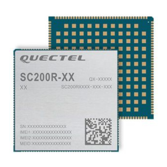
Figure 43: Top and Bottom Views of the Module NOTE Images above are for illustration purpose only and may differ from the actual module. For authentic appearance and label, please refer to the module received from Quectel. SC200R&SC262R_Series_Hardware_Design 114 / 124... -
Page 116: Storage, Manufacturing And Packaging
Smart Module Series Storage, Manufacturing and Packaging 9.1. Storage The module is provided with vacuum-sealed packaging. MSL of the module is rated as 3. The storage requirements are shown below. 1. Recommended Storage Condition: The temperature should be 23 ± 5 ° C and the relative humidity should be 35–60 %. - Page 117 Smart Module Series NOTES This floor life is only applicable when the environment conforms to IPC/JEDEC J-STD-033. It is recommended to start the solder reflow process within 24 hours after the package is removed if the temperature and moisture do not conform to, or are not sure to conform to IPC/JEDEC J-STD-033. And do not remove the packages of tremendous modules if they are not ready for soldering.
- Page 118 Smart Module Series Temp. (° C) Reflow Zone Max slope: Cooling down slope: 2~3 ° C/s -1.5 ~ -3 ° C/s Soak Zone Max slope: 1~3 ° C/s Figure 44: Recommended Reflow Soldering Thermal Profile Table 60: Recommended Thermal Profile Parameters Factor Recommendation Soak Zone...
- Page 119 PCB or shielding cover, and prevent the coating material from flowing into the module. 9.3. Packaging SC200R series module is packaged in tape and reel carriers, and sealed in the vacuum-sealed bag. It is not recommended to open the vacuum package before using the module for actual production. Each reel is 380 mm in diameter and contains 200 modules.
- Page 120 Smart Module Series Figure 46: Reel Dimensions (Unit: mm) Table 61: Reel Packaging Model MOQ for MP Minimum Package: 200 pcs Minimum Package × 4 = 800 pcs Name Size: 405 mm × 390 mm × 83 mm Size: 425 mm × 358 mm × 410 mm SC200R 200 pcs N.W.: 1.9 kg...
- Page 121 Smart Module Series Appendix References Table 62: Related Documents Document Name Description Quectel_Smart_EVB_G2_User_Guide Smart EVB G2 User Guide Quectel_SC200R_Series_Pin_Description_and SC200R Series Pin Description and GPIO _GPIO_Configuration Configuration Quectel_RF_Layout_Application_Note RF Layout Application Note Quectel_Module_Secondary_SMT_Application Module Secondary SMT Application Note _Note Quectel_SC200R_Series_Reference_Design...
- Page 122 Smart Module Series CDMA Code Division Multiple Access Circular Error Probable CMOS Complementary Metal-Oxide-Semiconductor Customer-Premise Equipment Coding Scheme Circuit Switched Data Camera Serial Interface Clear to Send Dual Carrier Digital Cellular System Downlink DPSK Differential Phase Shift Keying DQPSK Differential Quadrature Reference Phase Shift Keying Discontinuous Reception Display Serial Interface Digital Signal Processor...
- Page 123 Smart Module Series ETSI European Telecommunications Standards Institute Evaluation Board EV-DO/EVDO Evolution-Data Optimized EVRC Enhanced Variable Rate Codec Frequency Division Duplex Front End Module Frame per Second Full Rate GFSK Gaussian Frequency Shift Keying GLONASS Global Navigation Satellite System (Russia) GMSK Gaussian Minimum Shift Keying GNSS...
- Page 124 Smart Module Series HSUPA High Speed Uplink Packet Access High Throughput Integrated Circuit IEEE Institute of Electrical and Electronics Engineers Input/Output Inter-Integrated Circuit IMT-2000 International Mobile Telecommunications for the year 2000 Maximum Output Load Current Leadless Chip Carrier Liquid Crystal Display LCD Module Low Dropout Regulator Low Energy...
- Page 125 Smart Module Series Multi Purpose Pin Moisture Sensitivity Levels N.W. Net Weight Near Field Communication Negative Temperature Coefficient Over-the-Air Upgrade On-The-Go One Time Programable Power Amplifier Personal Computer Printed Circuit Board Power Control Level Personal Communication Service Personal Digital Assistant Protocol Data Unit Physical Layer Power Management Unit...
- Page 126 Smart Module Series RoHS Restriction of Hazardous Substances Real Time Clock Request to Send Surface Acoustic Wave Synchronous Connection Oriented Secure Digital SIMO Single Input Multiple Output Surface Mounting Device Short Message Service Surface Mount Technology Serial Peripheral Interface Station Time-Division Duplex Touch Panel TTFF...
- Page 127 Smart Module Series Voltage Input Minimum Input High Level Voltage Value Maximum Input Low Level Voltage Value Voltage Output Maximum Output Voltage Value Maximum Output High Level Voltage Value Minimum Output High Level Voltage Value Maximum Output Low Level Voltage Value WAPI WLAN Authentication and Privacy Infrastructure WCDMA...
Need help?
Do you have a question about the SC200R Series and is the answer not in the manual?
Questions and answers