Quectel SC20 Series Hardware Design
Hide thumbs
Also See for SC20 Series:
- User manual (30 pages) ,
- Manual (51 pages) ,
- Charging user manual (15 pages)

Related Manuals for Quectel SC20 Series


Summary of Contents for Quectel SC20 Series
- Page 1 SC20 Series Hardware Design Smart Module Series Version: 3.0.0 Date: 2021-07-30 Status: Preliminary...
- Page 2 To the maximum extent permitted by law, Quectel excludes all liability for any loss or damage suffered in connection with the use of the functions and features under development, regardless of whether such loss or damage may have been foreseeable.
- Page 3 Smart Module Series Copyright The information contained here is proprietary technical information of Quectel. Transmitting, reproducing, disseminating and editing this document as well as using the content without permission are forbidden. Offenders will be held liable for payment of damages. All rights are reserved in the event of a patent grant or registration of a utility model or design.
-
Page 4: Safety Information
Manufacturers of the cellular terminal should notify users and operating personnel of the following safety information by incorporating these guidelines into all manuals of the product. Otherwise, Quectel assumes no liability for customers’ failure to comply with these precautions. -
Page 5: About The Document
Added the frequency bands of SC20-E, SC20-A, SC20-AU and SC20-J modules (Tables 2, 3, 4 and 5) Added descriptions of Wi-Fi 5GHz frequency band (Tables 27, 28 and 35) Updated SC20 series operating frequencies Sea BAI/ (Table 33) 2017-10-17 Beny ZHU/... - Page 6 Smart Module Series Added the description that the GPIO_68 and GPIO_88 cannot be pulled up during start-up in Table 9 and Chapter 3.14. Updated the turning on timing of the module (Figure 8). Added the description for SPI interface in Chapter 3.14.
-
Page 7: Table Of Contents
Smart Module Series Contents Safety Information ............................3 About the Document ........................... 4 Contents ............................... 6 Table Index ..............................9 Figure Index ............................... 11 Introduction ............................13 Product Overview ..........................14 2.1. General Description ......................... 14 2.2. Key Features ........................... 17 2.3. - Page 8 Smart Module Series 3.21. Sensor Interfaces........................63 3.22. Audio Interfaces ........................64 3.22.1. Reference Circuit Design for Microphone Interface ............65 3.22.2. Reference Circuit Design for Earpiece Interface ............66 3.22.3. Reference Circuit Design for Headphone Interface ............66 3.22.4. Reference Circuit Design for Loudspeaker Interface............. 67 3.22.5.
- Page 9 Smart Module Series Storage, Manufacturing and Packaging ..................127 9.1. Storage Conditions ........................ 127 9.2. Manufacturing and Soldering ....................128 9.3. Packaging Specification ......................129 10 Appendix References ........................131 SC20_Series_Hardware_Design 8 / 133...
- Page 10 Smart Module Series Table Index Table 1: SC20-CE R1.1/-CEL R1.1 Frequency Bands ................14 Table 2: SC20-E/-EL/-EX Frequency Bands ....................15 Table 3: SC20-A/-AL/-AX Frequency Bands ....................15 Table 4: SC20-AU/-AUL Frequency Bands ....................16 Table 5: SC20-J/-JL Frequency Bands ...................... 16 Table 6: SC20-EU Frequency Bands ......................
- Page 11 Smart Module Series Table 42: Wi-Fi/Bluetooth Frequency ......................80 Table 43: Pin Definition of GNSS Antenna Interface ................. 81 Table 44: GNSS Frequency ........................82 Table 45: Antenna Requirements ....................... 85 Table 46: Absolute Maximum Ratings ......................89 Table 47: Module Power Supply Ratings ....................89 Table 48: Charging Performance Specifications ..................
- Page 12 Smart Module Series Figure Index Figure 1: Functional Diagram ........................21 Figure 2: Pin Assignment (Top View) ......................23 Figure 3: Voltage Drop Sample ........................35 Figure 4: Star Structure of the Power Supply ..................... 35 Figure 5: Reference Circuit of Power Supply ..................... 36 Figure 6: Turn on the Module Using Driving Circuit ...................
- Page 13 Smart Module Series Figure 42: Module Top and Side Dimensions ..................123 Figure 43: Module Bottom Dimensions (Top View) .................. 124 Figure 44: Recommended Footprint (Top View) ..................125 Figure 45: Top and Bottom Views of the Module ..................126 Figure 46: Recommended Reflow Soldering Thermal Profile ..............
-
Page 14: Introduction
Smart Module Series Introduction This document defines SC20 series module and its air interfaces and hardware interfaces which are related to your application. This document helps you quickly understand module interface specifications, electrical and mechanical details as well as other related information of the module. Associated with application notes and user guides, you can use the module to design and set up mobile applications easily. -
Page 15: Product Overview
Android version includes SC20-CE R1.1, SC20-E, SC20-A, SC20-AU, SC20-J, SC20-EU. Linux version includes SC20-CEL R1.1, SC20-EL, SC20-AL, SC20-AUL, SC20-JL, SC20-AX, SC20-EX. The following tables show the supported frequency bands and network standards of SC20 series. Table 1: SC20-CE R1.1/-CEL R1.1 Frequency Bands Mode Frequency LTE-FDD... - Page 16 Smart Module Series 900/1800 MHz 2400–2482 MHz Wi-Fi 802.11a/b/g/n 5180–5825 MHz Bluetooth 2402–2480 MHz GPS/Galileo: 1575.42 ±1.023 MHz GNSS GLONASS: 1597.5–1605.8 MHz BeiDou: 1561.098 ±2.046 MHz Table 2: SC20-E/-EL/-EX Frequency Bands Mode Frequency LTE-FDD B1/B3/B5/B7/B8/B20 LTE-TDD B38/B40/B41 WCDMA B1/B5/B8 850/900/1800/1900 MHz 2400–2482 MHz Wi-Fi 802.11a/b/g/n 5180–5825 MHz...
- Page 17 Smart Module Series BeiDou: 1561.098 ±2.046 MHz Table 4: SC20-AU/-AUL Frequency Bands Mode Frequency LTE-FDD B1/B3/B5/B7/B8/B28 LTE-TDD WCDMA B1/B2/B5/B8 850/900/1800/1900 MHz 2400–2482 MHz Wi-Fi 802.11a/b/g/n 5180–5825 MHz Bluetooth 4.2 LE 2402–2480 MHz GPS/Galileo: 1575.42 ±1.023 MHz GNSS GLONASS: 1597.5–1605.8 MHz BeiDou: 1561.098 ±2.046 MHz Table 5: SC20-J/-JL Frequency Bands Mode...
-
Page 18: Key Features
146 LCC pads and 64 LGA pads. With a compact profile of 40.5 mm × 40.5 mm × 2.8 mm, SC20 series can meet almost all requirements for M2M applications such as CPE, wireless POS, smart metering, router, data card, automotive, smart phone, digital signage, alarm panel, security and industry PDA, etc. - Page 19 Smart Module Series SC20-CE R1.1/-CEL R1.1, SC20-E/-EL, SC20-A/-AL, SC20-AU/-AUL, SC20-J/-JL, SC20-EU: 8 GB eMMC + 1 GB LPDDR3 (default) Memory 16 GB eMMC + 2 GB LPDDR3 (optional) SC20-AX, SC20-EX: 4 Gb NAND + 4 Gb LPDDR2 Operating System Android/Linux Supply voltage: 3.5–4.2 V Power Supply Typical supply voltage: 3.8 V...
- Page 20 Smart Module Series Downlink coding schemes: MCS 1–9 Uplink coding schemes: MCS 1–9 Max. 296 kbps (DL)/Max. 236.8 kbps (UL) Supports 2.4 GHz and 5 GHz frequency bands WLAN Features Supports 802.11a/b/g/n, maximally up to 150 Mbps Supports AP and STA modes Bluetooth Feature Bluetooth 4.2 LE GNSS Features...
-
Page 21: Functional Diagram
Firmware Upgrade Over USB interface RoHS All hardware components are fully compliant with EU RoHS directive 2.3. Functional Diagram The following figure shows a block diagram of SC20 series and illustrates the major functional parts. Power management Radio frequency ... -
Page 22: Evb
Figure 1: Functional Diagram 2.4. EVB To help you develop applications with the module, Quectel supplies the evaluation board (Smart EVB), USB to RS-232 converter cable, USB data cable, power adapter, earphone, antenna and other peripherals to control or test the module. For more details, see document [1]. -
Page 23: Application Interfaces
Smart Module Series Application Interfaces 3.1. General Description SC20 is a series of SMD type modules with 146 LCC pads and 64 LGA pads. The following chapters provide the detailed description of pins/interfaces listed below. Power supply VRTC interface ... -
Page 24: Pin Assignment
Smart Module Series 3.2. Pin Assignment The following figure shows the pin assignment of SC20 series. Figure 2: Pin Assignment (Top View) NOTE As for SC20-AX/EX, pins 105, 116, 117, 118, 119 are GPIO_15, GPIO_3, GPIO_2, GPIO_1 and GPIO_0 respectively. -
Page 25: Pin Description
Digital Output Digital Input/Output Open drain Power Input Power Output Power Input/Output The following table shows the pin definition and electrical characteristics of SC20 series. Table 9: Pin Description Power Supply Pin Name Description DC Characteristics Comment Power supply for Vmax = 4.2 V... - Page 26 Smart Module Series Power supply for Vnom = 1.8 V external GPIO’s LDO5_1V8 1.8 V output max = 20 mA pull-up and level shift circuits. Power supply for peripherals. If it is used, connect an external Vnom = 1.8 V LDO6_1V8 1.8 V output 2.2–4.7 μF...
- Page 27 Smart Module Series Speaker output SPKP SPKN Speaker output (-) Headphone right HPH_R channel output Headphone HPH_GND reference ground Headphone left HPH_L channel output Headset hot-plug High level by HS_DET detect default. USB Interface Pin Name Description DC Characteristics Comment USB 5 V power Vmax = 6.3 V 141,...
- Page 28 Smart Module Series max = 0.2 × USIM2_VDD Externally pull it up min = to USIM2_VDD USIM2_DATA (U)SIM2 card data 0.7 × USIM2_VDD with a 10 kΩ max = 0.4 V resistor. min = 0.8 × USIM2_VDD For 1.8 V (U)SIM: Vmax = 1.85 V Either 1.8 V or 2.95 Vmin = 1.75 V...
- Page 29 Smart Module Series max = 0.63 V If unused, keep UART1_RX UART1 receive min = 1.17 V these pins open. Connect to DTE’S CTS; DTE clear to send max = 0.63 V 1.8 V power UART1_CTS signal from DCE min = 1.17 V domain.
- Page 30 Smart Module Series 2.95 V SD card: SD_DATA2 SDIO data bit 2 max = 0.73 V min = 1.84 V max = 0.37 V SD_DATA3 SDIO data bit 3 min = 2.2 V SD card hot-plug max = 0.63 V SD_DET Active low.
- Page 31 Smart Module Series LCD MIPI data 1 MIPI_DSI_LN1P LCD MIPI data 2 MIPI_DSI_LN2N LCD MIPI data 2 MIPI_DSI_LN2P LCD MIPI data 3 MIPI_DSI_LN3N LCD MIPI data 3 MIPI_DSI_LN3P Camera Interfaces Pin Name Description DC Characteristics Comment Rear camera MIPI MIPI_CSI0_CLKN clock (-) Rear camera MIPI MIPI_CSI0_CLKP...
- Page 32 Smart Module Series Reset of front CAM1_RST camera Power down of CAM1_PWD front camera I2C clock of 1.8 V power CAM_I2C_SCL camera domain. I2C data of 1.8 V power CAM_I2C_SDA camera domain. Keypad Interfaces Pin Name Description DC Characteristics Comment Turns on/off the Internally pulled up PWRKEY...
- Page 33 Smart Module Series Pin Name Description DC Characteristics Comment Main antenna ANT_MAIN interface Rx-diversity ANT_DRX antenna interface 50 Ω impedance. GNSS antenna ANT_GNSS interface Wi-Fi/Bluetooth ANT_WIFI/BT antenna interface GPIO Interfaces Pin Name Description DC Characteristics Comment General-purpose GPIO_23 input/output General-purpose GPIO_32 input/output General-purpose...
- Page 34 Smart Module Series General-purpose GPIO_98 input/output General-purpose GPIO_94 input/output General-purpose GPIO_36 input/output General-purpose GPIO_65 input/output General-purpose GPIO_96 input/output General-purpose GPIO_58 input/output General-purpose GPIO_99 input/output General-purpose GPIO_95 input/output GPIO_11 General-purpose input/output GPIO_3 GPIO_10 General-purpose input/output GPIO_2 GPIO_9 General-purpose input/output GPIO_1 GPIO_8 General-purpose input/output GPIO_0...
-
Page 35: Power Supply
3.4.1. Power Supply Pins SC20 series provides two VBAT_RF pins and two VBAT_BB pins for connection with the external power supply. The VBAT_RF pins are used for the RF part of the module and the VBAT_BB pins are used for the baseband part of the module. - Page 36 Smart Module Series below 3.1 V. Figure 3: Voltage Drop Sample To decrease voltage drop, a bypass capacitor of about 100 µF with low ESR (ESR = 0.7 Ω) should be used, and a multi-layer ceramic chip capacitor (MLCC) should also be reserved due to its ultra-low ESR. It is recommended to use three ceramic capacitors (100 nF, 33 pF, 10 pF) for composing the MLCC array, and place these capacitors close to VBAT_BB/VBAT_RF pins.
-
Page 37: Reference Design For Power Supply
The power design for the module is very important, as the performance of module largely depends on the power source. The power supply of SC20 series should be able to provide enough current of at least 3 A. If the voltage drop between the input and output is not too high, it is suggested to use an LDO to supply power for the module. - Page 38 Smart Module Series Figure 6: Turn on the Module Using Driving Circuit The other way to control the PWRKEY is using a button directly. A TVS component is indispensable to be placed nearby the button for ESD protection. A reference circuit is shown in the following figure. Figure 7: Turn on the Module Using Keystroke The turning on scenario is illustrated in the following figure.
-
Page 39: Turn Off
Smart Module Series Figure 8: Timing of Turning on Module NOTE 1. When the module is powered on for the first time, its timing of turning on will be 45 ms longer than that shown above. 2. Make sure that VBAT is stable before pulling down PWRKEY pin. The recommended time between them is no less than 30 ms. -
Page 40: Vrtc Interface
Smart Module Series Figure 9: Timing of Turning off Module 3.6. VRTC Interface The RTC can be powered by an external power source through VRTC when the module is powered down and there is no power supply for the VBAT. The external power source can be a capacitor or rechargeable battery (such as coil cells) according to application demands. -
Page 41: Power Output
1.8/2.95 USIM2_VDD 1.8/2.95 3.8. Battery Charging and Management SC20 series can supports battery charging. The battery charger in the module supports trickle charging, constant current charging and constant voltage charging modes, which optimize the charging procedure for Li-ion batteries. SC20_Series_Hardware_Design... - Page 42 Smart Module Series Trickle charging: There are two steps in this mode. When the battery voltage is below 2.8 V, a 90 mA trickle charging current is applied to the battery. When the battery voltage is charged up and is between 2.8 V and 3.2 V, the charging current can be set to 450 mA maximally.
-
Page 43: Usb Interface
PMU. The input voltage of power supply ranges from 4.35 V to 6.3 V, and the typical value is 5.0 V. SC20 series supports charging management for a single Li-ion battery, but different charging parameters should be set for batteries with different models or capacities. - Page 44 Figure 14: USB Interface Reference Design (OTG is Supported) SC20 series supports OTG protocol. If OTG function is needed, see the above figure for the reference design. AW3605DNR is a high efficiency DC-DC chip manufactured by AWINIC, and you can also choose a suitable one according to your own demands.
-
Page 45: Uart Interfaces
Smart Module Series In order to ensure USB performance, comply with the following principles while designing USB interface. Route the USB signal traces as a differential pair with total grounding. The impedance of USB differential trace is 90 Ω. Keep the ESD protection devices as close as possible to the USB connector. - Page 46 Smart Module Series If unused, keep these pins open. UART2 receive; UART2_RX Debug port by default 1.8 V power domain. If it is unused, keep it open. UART2 transmit; UART2_TX Debug port by default UART1 provides 1.8 V logic level. A level translator should be used if your application is equipped with a 3.3 V UART interface.
-
Page 47: U)Sim Interfaces
UART2 is similar to UART1. For the reference design, see that of UART1. 3.11. (U)SIM Interfaces SC20 series provides two (U)SIM interfaces which meet ETSI and IMT-2000 requirements. Dual SIM Card Dual Standby is supported by default. Either 1.8 V or 2.95 V (U)SIM card is supported, and the (U)SIM card is powered by the internal power supply of the module. - Page 48 Smart Module Series SC20 series supports (U)SIM card hot-plug via the USIM_DETECT pin. A reference circuit for (U)SIM interface with an 8-pin (U)SIM card connector is shown below. Figure 17: Reference Circuit for (U)SIM Interface with an 8-pin (U)SIM Card Connector If there is no need to use USIM_DETECT for (U)SIM card hot-plug, keep it open.
-
Page 49: Sd Card Interface
RF interference, and they should be placed as close to the (U)SIM card connector as possible. 3.12. SD Card Interface The SD card interface of SC20 series supports SD 3.0 protocol and 4-bit SDIO. The pin definition is shown below. Table 15: Pin Definition of SD Card Interface Pin Name Pin No. - Page 50 Smart Module Series A reference circuit for SD card interface is shown below. Figure 19: Reference Circuit for SD Card Interface SD_LDO11 is the power supply for the external SD card. The maximum drive current is about 600 mA. Because of the high drive current, it is recommended that the trace width is 0.6 mm or more. In order to ensure the stability of drive power, a 2.2 μF capacitor should be added in parallel near the SD card connector.
-
Page 51: Gpio Interfaces
SD_DATA2 14.53 SD_DATA3 14.57 3.13. GPIO Interfaces SC20 series has abundant GPIO interfaces with logic level of 1.8 V. The pin definition is listed below. Table 17: Pin Definition of GPIO Interfaces Pin No. Pin Name GPIO No. Default state... - Page 52 Smart Module Series CAM0_RST GPIO_35 B-PD: nppukp Wakeup CAM0_PWD GPIO_34 B-PD: nppukp Wakeup CAM1_RST GPIO_28 B-PD: nppukp Wakeup CAM1_PWD GPIO_33 B-PD: nppukp CAM_I2C_SCL GPIO_30 B-PD: nppukp CAM_I2C_SDA GPIO_29 B-PD: nppukp GPIO_32 GPIO_32 B-PD: nppukp SENSOR_I2C_SCL GPIO_7 B-PD: nppukp SENSOR_I2C_SDA GPIO_6 B-PD: nppukp UART2_RX GPIO_5...
-
Page 53: Spi Interface
GPIO_0 GPIO_16 GPIO_16 B-PD: nppukp GPIO_17 GPIO_17 B-PD: nppukp NOTE For more details about GPIO configuration, see document [2]. 3.14. SPI Interface SC20 series provides one SPI interface multiplexed from GPIO interfaces. The interface only supports SC20_Series_Hardware_Design 52 / 133... -
Page 54: I2C Interfaces
GPIO_3 3.15. I2C Interfaces SC20 series provides three I2C interfaces which only support the master mode. As an open drain output, each I2C interface needs to be pulled up externally, and the recommended logic level is 1.8 V. Table 19: Pin Definition of I2C Interfaces Pin Name Pin No. -
Page 55: Adc Interfaces
Used for external sensor I2C data signal for external SENSOR_I2C_SDA sensor 3.16. ADC Interfaces SC20 series provides three analog-to-digital converter (ADC) interfaces, and the pin definition is shown below. Table 20: Pin Definition of ADC Interfaces Pin Name Pin No. -
Page 56: Lcm Interface
3.18. LCM Interface SC20 series provides one LCM interface, which is MIPI_DSI standard compliant. The interface supports high-speed differential data transmission with one 4-lane MIPI_DSI and a transmission rate of up to 1.5 Gbps/lane. It supports up to 720P resolution display. - Page 57 Smart Module Series 1.8 V power domain. LCD_RST LCD reset Active low. LCD_TE LCD tearing effect 1.8 V power domain. MIPI_DSI_CLKN LCD MIPI clock (-) MIPI_DSI_CLKP LCD MIPI clock (+) MIPI_DSI_LN0N LCD MIPI data 0 (-) MIPI_DSI_LN0P LCD MIPI data 0 (+) MIPI_DSI_LN1N LCD MIPI data 1 (-) MIPI_DSI_LN1P...
- Page 58 ADC pin, and please note that the output voltage of LCD_ID cannot exceed the voltage range of ADC pin. External backlight driving circuit needs to be designed for LCM, and a reference circuit design is shown in the following figure. Backlight brightness adjustment can be realized by PWM pin of SC20 series by adjusting the duty ratio.
-
Page 59: Touch Panel Interface
Smart Module Series 3.19. Touch Panel Interface SC20 series provides an I2C interface for connection with Touch Panel (TP), and it also provides the corresponding power supply and interrupt pins. The pin definition of TP interface is illustrated below. Table 23: Pin Definition of Touch Panel Interface Pin Name Pin No. -
Page 60: Camera Interfaces
Smart Module Series 3.20. Camera Interfaces Based on standard MIPI_CSI video input interface, SC20 series supports two cameras (2-lane + 1-lane), and the maximum pixel of the rear camera can be up to 8 MP. The video and photo quality are determined by various factors such as the camera sensor, camera lens quality, etc. -
Page 61: Front Camera Interface
Smart Module Series CAM0_RST Reset of rear camera CAM0_PWD Power down of rear camera CAM_I2C_SCL I2C clock of camera CAM_I2C_SDA I2C data of camera The following is a reference circuit design for rear camera interface, by taking the connection with T4KA3 camera as an example. - Page 62 Smart Module Series The pin definition of front camera interface is shown below. Table 25: Pin Definition of Front Camera Interface Pin Name Pin No. Description Comment 1.8 V output power supply for Vnom = 1.8 V LDO6_1V8 DOVDD of camera max = 100 mA 2.85 V output power supply for Vnom = 2.85 V...
-
Page 63: Design Considerations
Smart Module Series Figure 25: Reference Circuit Design for Front Camera Interface 3.20.3. Design Considerations Special attention should be paid to the definition of video device interfaces in schematic design. Different video devices will have varied definitions for their corresponding connectors. Ensure the device and the connectors are correctly connected. -
Page 64: Sensor Interfaces
0.40 MIPI_CSI0_LN0P 12.53 MIPI_CSI0_LN1N 13.73 0.76 MIPI_CSI0_LN1P 14.49 MIPI_CSI1_CLKN 17.32 0.13 MIPI_CSI1_CLKP 17.45 MIPI_CSI1_LN0N 18.89 0.35 MIPI_CSI1_LN0P 19.24 3.21. Sensor Interfaces SC20 series supports communication with sensors via an I2C interface, and it supports ALS/PS, compass, SC20_Series_Hardware_Design 63 / 133... -
Page 65: Audio Interfaces
Gravity sensor interrupt 2 GPIO_96 Gravity sensor interrupt 1 3.22. Audio Interfaces SC20 series provides two analog input channels and three analog output channels. The following table shows the pin definition. Table 28: Pin Definition of Audio Interfaces Pin Name Pin No. -
Page 66: Reference Circuit Design For Microphone Interface
Smart Module Series SPKP Speaker output (+) SPKN Speaker output (-) HPH_R Headphone right channel output HPH_GND Headphone reference ground HPH_L Headphone left channel output HS_DET Headset hot-plug detect High level by default. The module offers two audio input channels which are both single-ended channels. ... -
Page 67: Reference Circuit Design For Earpiece Interface
Smart Module Series 3.22.2. Reference Circuit Design for Earpiece Interface 33 pF EARP 33 pF EARN 33 pF Module Figure 27: Reference Circuit Design for Earpiece Interface 3.22.3. Reference Circuit Design for Headphone Interface Figure 28: Reference Circuit Design for Headphone Interface SC20_Series_Hardware_Design 66 / 133... -
Page 68: Reference Circuit Design For Loudspeaker Interface
Smart Module Series 3.22.4. Reference Circuit Design for Loudspeaker Interface Figure 29: Reference Circuit Design for Loudspeaker Interface 3.22.5. Audio Interfaces Design Considerations It is recommended to use the electret microphone with dual built-in capacitors (e.g. 10 pF and 33 pF) to filter out RF interference, thus reducing TDD noise. -
Page 69: Emergency Download Interface
Smart Module Series 3.23. Emergency Download Interface USB_BOOT is an emergency download interface. You can force the module to enter emergency download mode by pulling it up to LDO5_1V8 during power-up. This is an emergency option when failures such as abnormal start-up or running occur. For firmware upgrade and debugging in the future, reserve the following reference design. -
Page 70: Wi-Fi And Bluetooth
Wi-Fi and Bluetooth functions. 4.1. Wi-Fi Overview SC20 series module supports 2.4 GHz and 5 GHz dual-band WLAN wireless communication based on IEEE 802.11a/b/g/n standard protocols. The maximum data rate is up to 150 Mbps. - Page 71 Smart Module Series 802.11n HT20 MCS7 13 dBm ±2.5 dB 802.11n HT40 MCS0 14 dBm ±2.5 dB 802.11n HT40 MCS7 13 dBm ±2.5 dB Mode Output Power 802.11a 11 dBm ±2 dB WLAN 5.2GHz 802.11n-HT20 12 dBm ±2 dB 802.11n-HT40 11 dBm ±2.5 dB 802.11a 11 dBm ±2.5 dB...
-
Page 72: Bluetooth Overview
IEEE Std 802.11a, IEEE Std 802.11b, IEEE Std 802.11g: IEEE 802.11-2007 WLAN MAC and PHY, June 2007 4.2. Bluetooth Overview SC20 series supports Bluetooth 4.2 (BR/EDR + BLE) specification, as well as GFSK, 8-DPSK, π/4-DQPSK modulation modes. Maximally supports up to 7 wireless connections. ... -
Page 73: Bluetooth Performance
August 6, 2009 Bluetooth Low Energy RF PHY Test Specification, RF-PHY.TS/4.2.0, December 15, 2009 4.2.1. Bluetooth Performance The following table lists the Bluetooth transmitting and receiving performance of SC20 series. Table 32: Bluetooth Transmitting and Receiving Performance Transmitter Performance Packet Types... -
Page 74: Gnss
Smart Module Series GNSS SC20 series integrates a IZat™ GNSS engine (GEN 8C) which supports multiple positioning and navigation systems including GPS/BeiDou/GLONASS or GPS/BeiDou/Galileo. With an embedded LNA, the module provides greatly improved positioning accuracy. 5.1. GNSS Performance The following table lists the GNSS performance of the SC20 series in conduction mode. -
Page 75: Gnss Rf Design Guidelines
Smart Module Series 5.2. GNSS RF Design Guidelines Bad design of antenna and layout may cause reduced GNSS receiving sensitivity, longer GNSS positioning time, or reduced positioning accuracy. In order to avoid this, follow the reference design rules as below: Maximize the distance between the GNSS RF part and the GPRS RF part (including trace routing ... -
Page 76: Antenna Interfaces
Smart Module Series Antenna Interfaces SC20 series provides four antenna interfaces for the main antenna, Rx-diversity antenna, GNSS antenna and Wi-Fi/Bluetooth antenna, respectively. The antenna ports have an impedance of 50 Ω. 6.1. Main/Rx-diversity Antenna Interfaces The pin definition of main/Rx-diversity antenna interfaces is shown below. - Page 77 Smart Module Series LTE-FDD B1 2110–2170 1920–1980 LTE-FDD B3 1805–1880 1710–1785 LTE-FDD B5 869–894 824–849 LTE-FDD B8 925–960 880–915 LTE-TDD B38 2570–2620 2570–2620 LTE-TDD B39 1880–1920 1880–1920 LTE-TDD B40 2300–2400 2300–2400 LTE-TDD B41 2555–2655 2555–2655 Table 36: SC20-E/-EL/-EX Operating Frequencies 3GPP Band Receive Transmit...
- Page 78 Smart Module Series LTE-TDD B38 2570–2620 2570–2620 LTE-TDD B40 2300–2400 2300–2400 LTE-TDD B41 2555–2655 2555–2655 Table 37: SC20-A/-AL/-AX Operating Frequencies 3GPP Band Receive Transmit Unit GSM850 869–894 824–849 PCS1900 1930–1990 1850–1910 WCDMA B1 2110–2170 1920–1980 WCDMA B2 1930–1990 1850–1910 WCDMA B4 2110–2155 1710–1755 WCDMA B5...
- Page 79 Smart Module Series Table 38: SC20-AU/-AUL Operating Frequencies 3GPP Band Receive Transmit Unit GSM850 869–894 824–849 EGSM900 925–960 880–915 DCS1800 1805–1880 1710–1785 PCS1900 1930–1990 1850–1910 WCDMA B1 2110–2170 1920–1980 WCDMA B2 1930–1990 1850–1910 WCDMA B5 869–894 824–849 WCDMA B8 925–960 880–915 LTE-FDD B1 2110–2170...
- Page 80 Smart Module Series LTE-FDD B8 925–960 880–915 LTE-FDD B18 860–875 815–830 LTE-FDD B19 875–890 830–845 LTE-FDD B26 859–894 814–849 LTE-TDD B41 2545–2655 2545–2655 Table 40: SC20-EU Module Operating Frequencies 3GPP Band Receive Transmit Unit GSM850 869–894 824–849 EGSM900 925–960 880–915 DCS1800 1805–1880 1710–1785...
-
Page 81: Main And Rx-Diversity Antenna Interfaces Reference Design
Smart Module Series 6.1.2. Main and Rx-diversity Antenna Interfaces Reference Design A reference circuit design for main and Rx-diversity antenna interfaces is shown below. Reserve a π-type matching circuit for each antenna to achieve better RF performance, and place the π-type matching components (R1/C1/C2, R2/C3/C4) as close to the antennas as possible. -
Page 82: Gnss Antenna Interface
Smart Module Series 5180–5825 Bluetooth 4.2 LE 2402–2480 NOTE The supported Wi-Fi frequencies of SC20-J/-JL are 2400–2496 MHz and 5180–5825 MHz. A reference circuit design for Wi-Fi/Bluetooth antenna interface is shown as below. A π-type matching circuit should be reserved for better RF performance. The π-type matching components (R1, C1, C2) should be placed as close to the antenna as possible and are mounted according to the actual debugging. -
Page 83: Recommended Circuit For Passive Antenna
Smart Module Series Table 44: GNSS Frequency Type Frequency Unit GPS/Galileo 1575.42 ±1.023 GLONASS 1597.5–1605.8 BeiDou 1561.098 ±2.046 6.3.1. Recommended Circuit for Passive Antenna GNSS antenna interface supports passive ceramic antennas and other types of passive antennas. A reference circuit design is given below. Figure 33: Reference Circuit Design for GNSS Passive Antenna NOTE When the passive antenna is placed far away from the module (that is, the antenna trace is long), it is... -
Page 84: Reference Design For Rf Layout
Smart Module Series Figure 34: Reference Circuit Design for GNSS Active Antenna 6.4. Reference Design for RF Layout For user’s PCB, the characteristic impedance of all RF traces should be controlled to 50 Ω. The impedance of the RF traces is usually determined by the trace width (W), the materials’ dielectric constant, the height from the reference ground to the signal layer (H), and the spacing between RF traces and grounds (S). - Page 85 Smart Module Series Figure 36: Coplanar Waveguide Design on a 2-layer PCB Figure 37: Coplanar Waveguide Design on a 4-layer PCB (Layer 3 as Reference Ground) Figure 38: Coplanar Waveguide Design on a 4-layer PCB (Layer 4 as Reference Ground) SC20_Series_Hardware_Design 84 / 133...
-
Page 86: Antenna Installation
Smart Module Series In order to ensure RF performance and reliability, follow the principles below in RF layout design: Use an impedance simulation tool to accurately control the characteristic impedance of RF traces to 50 Ω. Design the GND pins adjacent to RF pins as thermal relief pads, and fully connect them to ground. ... -
Page 87: Recommended Rf Connector For Antenna Installation
Smart Module Series Cable Insertion Loss: < 1 dB (GSM850, EGSM900, WCDMA B5/B6/B8/B19, EVDO/CDMA BC0, LTE-FDD B5/B8/B12/B13/B18/B19/B20/B26/B28) Cable Insertion Loss: < 1.5 dB (DCS1800, PCS1900, WCDMA B1/B2/B4, TD-SCDMA B34/B39, LTE-FDD B1/B2/B3/B4/B25, LTE-TDD B39) Cable Insertion Loss: < 2 dB (LTE-FDD B7, LTE-TDD B38/B40/B41) VSWR: ≤... - Page 88 Smart Module Series Figure 39: Dimensions of the U.FL-R-SMT Connector (Unit: mm) U.FL-LP serial connectors listed in the following figure can be used to match the U.FL-R-SMT. Figure 40: Mechanicals of U.FL-LP Connectors The following figure describes the space factor of the mated connector. SC20_Series_Hardware_Design 87 / 133...
- Page 89 Smart Module Series Figure 41: Space Factor of Mated Connectors (Unit: mm) For more details, visit http://www.hirose.com. SC20_Series_Hardware_Design 88 / 133...
-
Page 90: Reliability, Radio And Electrical Characteristics
Smart Module Series Reliability, Radio and Electrical Characteristics 7.1. Absolute Maximum Ratings Absolute maximum ratings for power supply and voltage on digital and analog pins of the module are listed in the following table. Table 46: Absolute Maximum Ratings Parameter Min. -
Page 91: Charging Performance Specifications
Smart Module Series Peak supply Maximum power control level current (during VBAT at EGSM900. transmission slot) USB_VBUS USB detection 4.35 Power supply VRTC voltage of the 3.25 backup battery 7.3. Charging Performance Specifications Table 48: Charging Performance Specifications Parameter Min. Typ. -
Page 92: Operating And Storage Temperatures
Smart Module Series 7.4. Operating and Storage Temperatures The operating temperature is listed in the following table. Table 49: Operating and Storage Temperatures Parameter Min. Typ. Max. Unit Operating temperature range ºC Storage Temperature Range ºC 7.5. Power Consumption The values of current consumption are shown below. Table 50: SC20-CE R1.1/-CEL R1.1 Current Consumption Description Conditions... - Page 93 Smart Module Series supply current @ DRX = 5 Sleep (USB disconnected) 3.83 @ DRX = 6 Sleep (USB disconnected) 3.02 @ DRX = 7 Sleep (USB disconnected) 2.65 @ DRX = 8 Sleep (USB disconnected) 5.49 @ DRX = 5 Sleep (USB disconnected) 3.87 @ DRX = 6...
- Page 94 Smart Module Series DCS1800 (2UL/3DL) @ 24.74 dBm DCS1800 (3UL/2DL) @ 24.54 dBm DCS1800 (4UL/1DL) @ 24.44 dBm EVDO/CDMA BC0 (max power) @ 23.68 dBm data transfer B1 (HSDPA) @ 21.64 dBm B8 (HSDPA) @ 21.61 dBm WCDMA data transfer B1 (HSUPA) @ 21.36 dBm B8 (HSUPA) @ 21.56 dBm LTE-FDD B1 @ 22.96 dBm...
- Page 95 Smart Module Series Sleep (USB disconnected) 2.35 @ DRX = 7 Sleep (USB disconnected) 2.01 @ DRX = 8 Sleep (USB disconnected) 1.85 @ DRX = 9 Sleep (USB disconnected) 5.51 @ DRX = 5 Sleep (USB disconnected) 3.56 @ DRX = 6 LTE-FDD supply current Sleep (USB disconnected)
- Page 96 Smart Module Series PCS1900 151.3 PCL = 7 @ 16.72 dBm PCS1900 130.0 PCL = 15 @ 0.98 dBm B1 (max power) @ 23.18 dBm 544.1 WCDMA voice call B5 (max power) @ 23.22 dBm 513.5 B8 (max power) @ 23.29 dBm 522.7 GSM850 (1UL/4DL) @ 33.12 dBm 265.9...
- Page 97 Smart Module Series EGSM900 (1UL/4DL) @ 27.05 dBm EGSM900 (2UL/3DL) @ 27.13 dBm 177.4 EGSM900 (3UL/2DL) @ 27.28 dBm 278.3 EGSM900 (4UL/1DL) @ 27.19 dBm 371.0 DCS1800 (1UL/4DL) @ 26.04 dBm 170.6 DCS1800 (2UL/3DL) @ 25.98 dBm 260.5 DCS1800 (3UL/2DL) @ 25.71 dBm 349.8 DCS1800 (4UL/1DL) @ 25.46 dBm 440.2...
- Page 98 Smart Module Series LTE-TDD B40 @ 23.17 dBm LTE-TDD B41 @ 23.19 dBm Table 52: SC20-EX Current Consumption Description Conditions Typ. Unit OFF state Power down μA Sleep (USB disconnected) 4.524 @ DRX = 2 GSM/GPRS Sleep (USB disconnected) 3.212 supply current @ DRX = 5 Sleep (USB disconnected)
- Page 99 Smart Module Series GSM850 166.5 PCL = 12 @ 19.15 dBm GSM850 114.67 PCL = 19 @ 5.31 dBm EGSM900 327.32 PCL = 5 @ 33.07 dBm EGSM900 168.33 PCL = 12 @ 19.53 dBm EGSM900 115.63 PCL = 19 @ 5.59 dBm DCS1800 235.97 PCL = 0 @ 30.00 dBm...
- Page 100 Smart Module Series DCS1800 (2UL/3DL) @ 29.86 dBm 299.56 DCS1800 (3UL/2DL) @ 29.73 dBm 373.98 DCS1800 (4UL/1DL) @ 29.63 dBm 450.69 PCS1900 (1UL/4DL) @ 29.77 dBm PCS1900 (2UL/3DL) @ 29.64 dBm 303.21 PCS1900 (3UL/2DL) @ 29.54 dBm 366.81 PCS1900 (4UL/1DL) @ 29.34 dBm 451.51 GSM850 (1UL/4DL) @ 26.75 dBm 235.97...
- Page 101 Smart Module Series B8 (HSDPA) @ 22.24 dBm 533.04 B1 (HSUPA) @ 22.30 dBm 593.77 B5 (HSUPA) @ 21.93 dBm 535.61 B8 (HSUPA) @ 21.90 dBm 542.95 LTE-FDD B1 @ 23.29 dBm 778.16 LTE-FDD B3 @ 23.29 dBm 808.09 LTE-FDD B5 @ 23.44 dBm 622.64 LTE-FDD B7 @ 23.28 dBm 862.03...
- Page 102 Smart Module Series Sleep (USB disconnected) 6.60 @ DRX = 5 Sleep (USB disconnected) 4.24 @ DRX = 6 LTE-FDD supply current Sleep (USB disconnected) 3.11 @ DRX = 7 Sleep (USB disconnected) 2.77 @ DRX = 8 GSM850 254.60 PCL = 5 @ 32.23 dBm GSM850 136.30...
- Page 103 Smart Module Series GSM850 (1UL/4DL) @ 26.39 dBm 186.00 GSM850 (2UL/3DL) @ 26.30 dBm 280.00 GSM850 (3UL/2DL) @ 26.30 dBm 368.00 GSM850 (4UL/1DL) @ 26.07 dBm 456.00 EDGE data transfer PCS1900 (1UL/4DL) @ 25.70 dBm 184.40 PCS1900 (2UL/3DL) @ 25.55 dBm 276.60 PCS1900 (3UL/2DL) @ 25.39 dBm 365.20...
- Page 104 Smart Module Series LTE-FDD B26 @ 23.57 dBm 718.75 Table 54: SC20-AX Current Consumption Description Conditions Typ. Unit OFF state Power down μA Sleep USB disconnected) @ DRX = 2 GSM/GPRS Sleep (USB disconnected) supply current @ DRX = 5 Sleep (USB disconnected) @ DRX = 9 Sleep (USB disconnected)
- Page 105 Smart Module Series B1 (max power) @ 23.41 dBm 611.94 B2 (max power) @ 23.27 dBm 625.14 WCDMA voice call B4 (max power) @ 23.44 dBm 567.13 B5 (max power) @ 23.4 dBm 583.06 B8 (max power) @ 23.32 dBm 556.48 GSM850 (1UL/4DL) @ 33.34 dBm 295.23...
- Page 106 Smart Module Series B8 (HSDPA) @ 23.1 dBm 540.98 B1 (HSUPA) @ 22.66 dBm 616.34 B2 (HSUPA) @ 22.38 dBm 654.26 B4 (HSUPA) @ 21.56 dBm 594.59 B5 (HSUPA) @ 22.25 dBm 575.03 B8 (HSUPA) @ 22.34 dBm 549.07 LTE-FDD B2 @ 23.11 dBm 790.67 LTE-FDD B4 @ 23.44 dBm 749.6...
- Page 107 Smart Module Series Sleep (USB disconnected) 1.75 @ DRX = 9 Sleep (USB disconnected) 5.29 @ DRX = 5 Sleep (USB disconnected) 3.59 @ DRX = 6 LTE-FDD supply current Sleep (USB disconnected) 2.76 @ DRX = 7 Sleep (USB disconnected) 2.24 @ DRX = 8 Sleep (USB disconnected)
- Page 108 Smart Module Series B1 (max power) @ 23.33 dBm B2 (max power) @ 23.51 dBm WCDMA voice call B5 (max power) @ 23.37 dBm B8 (max power) @ 23.38 dBm GSM850 (1UL/4DL) @ 32.91 dBm GSM850 (2UL/3DL) @ 32.26 dBm GSM850 (3UL/2DL) @ 30.72 dBm GSM850 (4UL/1DL) @ 29.38 dBm EGSM900 (1UL/4DL) @ 32.92 dBm...
- Page 109 Smart Module Series EGSM900 (2UL/3DL) @ 27.27 dBm EGSM900 (3UL/2DL) @ 26.85 dBm EGSM900 (4UL/1DL) @ 26.53 dBm DCS1800 (1UL/4DL) @ 25.39 dBm DCS1800 (2UL/3DL) @ 25.40 dBm DCS1800 (3UL/2DL) @ 25.35 dBm DCS1800 (4UL/1DL) @ 25.05 dBm PCS1900 (1UL/4DL) @ 26.03 dBm PCS1900 (2UL/3DL) @ 26.07 dBm PCS1900 (3UL/2DL) @ 25.81 dBm PCS1900 (4UL/1DL) @ 25.70 dBm...
- Page 110 Smart Module Series LTE-TDD B40 @ 23.24 dBm Table 56: SC20-J/-JL Current Consumption Description Conditions Typ. Unit OFF state Power down μA Sleep (USB disconnected) 3.07 @ DRX = 6 Sleep (USB disconnected) 2.41 @ DRX = 7 WCDMA supply current Sleep (USB disconnected) 2.11 @ DRX = 8...
- Page 111 Smart Module Series B8 (HSDPA) @ 22.17 dBm B19 (HSDPA) @ 22.31 dBm B1 (HSUPA) @ 21.4 dBm B6 (HSUPA) @ 22.05 dBm B8 (HSUPA) @ 21.57 dBm B19 (HSUPA) @ 22.14 dBm LTE-FDD B1 @ 23.64 dBm LTE-FDD B3 @ 23.52 dBm LTE-FDD B8 @ 23.40 dBm LTE data transfer LTE-FDD B18 @ 23.45 dBm...
- Page 112 Smart Module Series supply current Sleep (USB disconnected) DRX = 6 3.56 Sleep (USB disconnected) DRX = 7 2.62 Sleep (USB disconnected) DRX = 8 2.14 Sleep (USB disconnected) DRX = 5 5.93 Sleep (USB disconnected) DRX = 6 3.74 LTE-TDD supply current Sleep (USB disconnected) DRX = 7...
- Page 113 Smart Module Series GSM850 (1UL/4DL) @ 32.45 dBm GSM850 (2UL/3DL) @ 32.27 dBm GSM850 (3UL/2DL) @ 30.12 dBm GSM850 (4UL/1DL) @ 29.17 dBm EGSM900 (1UL/4DL) @ 32.82 dBm EGSM900 (2UL/3DL) @ 32.63 dBm EGSM900 (3UL/2DL) @ 30.69 dBm EGSM900 (4UL/1DL) @ 29.72 dBm GPRS data transfer DCS1800 (1UL/4DL) @ 29.76 dBm...
- Page 114 Smart Module Series DCS1800 (2UL/3DL) @ 25.64 dBm DCS1800 (3UL/2DL) @ 23.52 dBm DCS1800 (4UL/1DL) @ 22.37 dBm PCS1900 (1UL/4DL) @ 26.13 dBm PCS1900 (2UL/3DL) @ 25.95 dBm PCS1900 (3UL/2DL) @ 23.62 dBm PCS1900 (4UL/1DL) @ 22.46 dBm B1 (HSDPA) @ 22.48 dBm B2 (HSDPA) @ 22.45 dBm B5 (HSDPA) @ 22.41 dBm B8 (HSDPA) @ 22.41 dBm...
-
Page 115: Tx Power
Smart Module Series 7.6. Tx Power The following table shows the RF output power of the SC20 series. Table 58: RF Output Power Frequency Bands Max. RF Output Power Min. RF Output Power GSM850 33 dBm ±2 dB 5 dBm ±5 dB EGSM900 33 dBm ±2 dB... -
Page 116: Rx Sensitivity
In GPRS 4-slot Tx mode, the maximum output power is reduced by 3 dB. This design conforms to the GSM specification as described in Chapter 13.16 of 3GPP TS 51.010-1. 7.7. Rx Sensitivity The following table shows the RF receiving sensitivity of the SC20 series. Table 59: SC20-CE R1.1/-CEL R1.1 RF Receiving Sensitivity Receiving Sensitivity (Typ.) - Page 117 Smart Module Series DCS1800 -109 dBm -102 dBm WCDMA B1 -110 dBm -106.7 dBm WCDMA B8 -110 dBm -103.7 dBm EVDO-CDMA BC0 -108 dBm -104 dBm TD-SCDMA B34 -113 dBm -108 dBm TD-SCDMA B39 -113 dBm -108 dBm LTE-FDD B1 (10 MHz) -98 dBm -99.1 dBm -100.6 dBm...
- Page 118 Smart Module Series LTE-FDD B1 (10 MHz) -98 dBm -99 dBm -102 dBm -96.3 dBm LTE-FDD B3 (10 MHz) -97 dBm -98 dBm -101 dBm -93.3 dBm LTE-FDD B5 (10 MHz) -99 dBm -98 dBm -102 dBm -94.3 dBm LTE-FDD B7 (10 MHz) -97 dBm -97 dBm -102 dBm...
- Page 119 Smart Module Series LTE-FDD B20 (10 MHz) -98.1 dBm -99.4 dBm -101.7 dBm -93.3 dBm LTE-TDD B38 (10 MHz) -95.9 dBm -96.8 dBm -99.1 dBm -96.3 dBm LTE-TDD B40 (10 MHz) -96.5 dBm -97.5 dBm -99.8 dBm -96.3 dBm LTE-TDD B41 (10 MHz) -95.5 dBm -95.1 dBm -98.3 dBm...
- Page 120 Smart Module Series Table 63: SC20-AX RF Receiving Sensitivity Receiving Sensitivity (Typ.) Frequency Bands 3GPP (SIMO) Primary Diversity SIMO GSM850 -110.0dBm -102 dBm PCS1900 -108.9 dBm -102 dBm WCDMA B1 -109.5 dBm -110.8 dBm -112.8 dBm -106.7 dBm WCDMA B2 -110.2 dBm -110.7 dBm -112.7 dBm...
- Page 121 Smart Module Series PCS1900 -109 dBm -102 dBm WCDMA B1 -110 dBm -110 dBm -113 dBm -106.7 dBm WCDMA B2 -110 dBm -104.7 dBm WCDMA B5 -110 dBm -110 dBm -113 dBm -104.7 dBm WCDMA B8 -110 dBm -110 dBm -113 dBm -103.7 dBm LTE-FDD B1 (10 MHz)
- Page 122 Smart Module Series LTE-TDD B26 (10 MHz) -98 dBm -99 dBm -101.5 dBm -93.8 dBm LTE-TDD B41 (10 MHz) -96 dBm -96.5 dBm -100 dBm -94.3 dBm Table 66: SC20-EU RF Receiving Sensitivity Receiving Sensitivity (Typ.) Frequency Bands 3GPP (SIMO) Primary Diversity SIMO...
-
Page 123: Esd
The following table shows the electrostatic discharge characteristics of the SC20 series. Table 67: ESD Characteristics (Temperature: 25 ºC, Humidity: 45 %) -
Page 124: Mechanical Information
Smart Module Series Mechanical Information This chapter describes the mechanical dimensions of the module. All dimensions are measured in millimeter (mm), and the tolerances for dimensions without tolerance values are ±0.2 mm. 8.1. Mechanical Dimensions Figure 42: Module Top and Side Dimensions SC20_Series_Hardware_Design 123 / 133... - Page 125 Smart Module Series Figure 43: Module Bottom Dimensions (Top View) NOTE The package warpage level of the module conforms to JEITA ED-7306 standard. SC20_Series_Hardware_Design 124 / 133...
-
Page 126: Recommended Footprint
Smart Module Series 8.2. Recommended Footprint Figure 44: Recommended Footprint (Top View) NOTE For easy maintenance of the module, keep at least 5 mm between the module and other components on the host PCB. All RESERVED pins should be kept open and MUST NOT be connected to ground. SC20_Series_Hardware_Design 125 / 133... -
Page 127: Top And Bottom Views
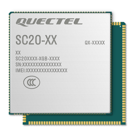
Figure 45: Top and Bottom Views of the Module NOTE Images above are for illustration purpose only and may differ from the actual module. For authentic appearance and label, please refer to the module received from Quectel. SC20_Series_Hardware_Design 126 / 133... -
Page 128: Storage, Manufacturing And Packaging
Smart Module Series Storage, Manufacturing and Packaging 9.1. Storage Conditions The module is provided with vacuum-sealed packaging. MSL of the module is rated as 3. The storage requirements are shown below. 1. Recommended Storage Condition: The temperature should be 23 ±5 °C and the relative humidity should be 35–60 %. -
Page 129: Manufacturing And Soldering
Smart Module Series put in a dry environment such as in a drying oven. NOTE 1. To avoid blistering, layer separation and other soldering issues, extended exposure of the module to the air is forbidden. 2. Take out the module from the package and put it on high-temperature-resistant fixtures before baking. All modules must be soldered to PCB within 24 hours after the baking, otherwise put them in the drying oven. -
Page 130: Packaging Specification
(e.g. selective soldering) that is not mentioned in document [4]. 9.3. Packaging Specification SC20 series is packaged in tape and reel carriers. Each reel is 12.32 meters long and contains 200 modules. The following figures show the package details, measured in mm. SC20_Series_Hardware_Design... - Page 131 Smart Module Series Figure 47: Tape Dimensions Figure 48: Reel Dimensions Table 69: Reel Packaging Model MOQ for MP Minimum Package: 200 pcs Minimum Package × 4 = 800 pcs Name Size: 370 mm × 350 mm × 85 mm Size: 380 mm ×...
-
Page 132: Appendix References
Smart Module Series Appendix References Table 70: Related Documents Document Name [1] Quectel_Smart_EVB_User_Guide [2] Quectel_SC20_Series_GPIO_Configuration [3] Quectel_RF_Layout_Application_Note [4] Quectel_Module_Secondary_SMT_Application_Note [5] Quectel_SC20_Series_Reference_Design Table 71: Terms and Abbreviations Abbreviation Description Analog-to-Digital Converter Adaptive Multi-rate Access Point Bits per Second CDMA Code Division Multiple Access Coding Scheme Circuit Switched Data Camera Serial Interface... - Page 133 Smart Module Series Discontinuous Reception Display Serial Interface Digital Signal Processor EDGE Enhanced Data Rate for GSM Evolution Enhanced Full Rate EGSM Enhanced GSM eSCO Extended Synchronous Connection Oriented Electrostatic Discharge Equivalent Series Resistance Frequency Division Duplex Full Rate GMSK Gaussian Minimum Shift Keying GNSS Global Navigation Satellite System...
- Page 134 Smart Module Series Inter-Integrated Circuit Leadless Chip Carrier Liquid Crystal Display LCD Module Low Dropout Regulator Low Energy Light Emitting Diode Land Grid Array Low Noise Amplifier Long-Term Evolution Modulation and Coding Scheme MIPI Mobile Industry Processor Interface Negative Temperature Coefficient Printed Circuit Board Protocol Data Unit Pulse Width Modulation...
- Page 135 Smart Module Series SD Card Secure Digital Card Short Message Service Serial Peripheral Interface Time-Division Duplex Touch Panel Transient Voltage Suppressor Transmit UART Universal Asynchronous Receiver & Transmitter UMTS Universal Mobile Telecommunications System Universal Serial Bus (U)SIM (Universal) Subscriber Identity Module VBAT Voltage at Battery (Pin) Vmax...
- Page 136 Smart Module Series FCC Certification Requirements. According to the definition of mobile and fixed device is described in Part 2.1091(b), this device is a mobile device. And the following conditions must be met: 1. This Modular Approval is limited to OEM installation for mobile and fixed applications only. The antenna installation and operating configurations of this transmitter, including any applicable source-based timeaveraging duty factor, antenna gain and cable loss must satisfy MPE categorical Exclusion Requirements of 2.1091.
- Page 137 Smart Module Series If the device is used for other equipment that separate approval is required for all other operating configurations, including portable configurations with respect to 2.1093 and different antenna configurations. For this device, OEM integrators must be provided with labeling instructions of finished products. Please refer to KDB784748 D01 v07, section 8.
- Page 138 Smart Module Series interference, including interference that may cause undesired operation of the device." or "Le présent appareil est conforme aux CNR d’Industrie Canada applicables aux appareils radio exempts de licence. L’exploitation est autorisée aux deux conditions suivantes : 1) l’appareil ne doit pas produire de brouillage; 2) l’utilisateur de l’appareil doit accepter tout brouillage radioélectrique subi, même si le brouillage est susceptible d’en compromettre le fonctionnement."...
Need help?
Do you have a question about the SC20 Series and is the answer not in the manual?
Questions and answers