
Related Manuals for Quectel SC600Y-NA Series


Summary of Contents for Quectel SC600Y-NA Series
- Page 1 SC600Y&SC600T Hardware Design Smart LTE Module Series Rev: SC600Y&SC600T_Hardware_Design_V1.0 Date: 2019-07-01 Status: Preliminary www.quectel.com...
- Page 2 QUECTEL OFFERS THE INFORMATION AS A SERVICE TO ITS CUSTOMERS. THE INFORMATION PROVIDED IS BASED UPON CUSTOMERS’ REQUIREMENTS. QUECTEL MAKES EVERY EFFORT TO ENSURE THE QUALITY OF THE INFORMATION IT MAKES AVAILABLE. QUECTEL DOES NOT MAKE ANY WARRANTY AS TO THE INFORMATION CONTAINED HEREIN, AND DOES NOT ACCEPT ANY LIABILITY FOR ANY INJURY, LOSS OR DAMAGE OF ANY KIND INCURRED BY USE OF OR RELIANCE UPON THE INFORMATION.
-
Page 3: About The Document
Smart LTE Module Series SC600Y&SC600T Hardware Design About the Document History Revision Date Author Description Light WANG/ 2019-07-01 Initial Rock CHEN SC600Y&SC600T_Hardware_Design 2 / 128... -
Page 4: Table Of Contents
Smart LTE Module Series SC600Y&SC600T Hardware Design Contents About the Document ........................... 2 Contents ............................... 3 Table Index ..............................6 Figure Index ..............................8 Introduction ............................14 1.1. Safety Information ........................15 Product Concept ..........................16 2.1. General Description ........................16 2.2. - Page 5 Smart LTE Module Series SC600Y&SC600T Hardware Design 3.21.1. Design Considerations ....................77 3.21.2. Flashlight Interfaces ....................... 79 3.22. Sensor Interfaces ........................80 3.23. Audio Interfaces ........................80 3.23.1. Reference Circuit Design for Microphone Interfaces ............. 82 3.23.2. Reference Circuit Design for Earpiece Interface ............83 3.23.3.
- Page 6 Smart LTE Module Series SC600Y&SC600T Hardware Design Storage, Manufacturing and Packaging ..................122 9.1. Storage ............................ 122 9.2. Manufacturing and Soldering ....................123 9.3. Packaging ..........................124 10 Appendix A References ........................126 11 Appendix B GPRS Coding Schemes ..................... 129 12 Appendix C GPRS Multi-slot Classes ....................
- Page 7 Smart LTE Module Series SC600Y&SC600T Hardware Design Table Index TABLE 1: SC600Y-EM*/SC600T-EM* FREQUENCY BANDS ................16 TABLE 2: SC600Y-NA*/SC600T-NA* FREQUENCY BANDS ................17 TABLE 3: SC600Y-JP*/SC600T-JP* FREQUENCY BANDS ................17 TABLE 4: SC600Y-WF*/SC600T-WF* FREQUENCY BANDS ................18 TABLE 5: SC600Y&SC600T KEY FEATURES ....................19 TABLE 6: I/O PARAMETERS DEFINITION .......................
- Page 8 Smart LTE Module Series SC600Y&SC600T Hardware Design TABLE 42: ANTENNA REQUIREMENTS ......................100 TABLE 43: ABSOLUTE MAXIMUM RATINGS ....................103 TABLE 44: SC600Y&SC600T MODULES POWER SUPPLY RATINGS ............103 TABLE 45: OPERATION AND STORAGE TEMPERATURES ................ 104 TABLE 46: SC600Y-JP*/SC600T-JP* CURRENT CONSUMPTION ............... 105 TABLE 47: SC600Y-EM*/SC600T-EM* CURRENT CONSUMPTION ............
- Page 9 Smart LTE Module Series SC600Y&SC600T Hardware Design Figure Index FIGURE 1: FUNCTIONAL DIAGRAM ....................... 23 FIGURE 2: PIN ASSIGNMENT (TOP VIEW)..................... 26 FIGURE 3: VOLTAGE DROP SAMPLE ......................43 FIGURE 4: STAR STRUCTURE OF POWER SUPPLY ..................44 FIGURE 5: REFERENCE CIRCUIT OF POWER SUPPLY ................45 FIGURE 6: TURN ON THE MODULE USING DRIVING CIRCUIT ..............
- Page 10 Smart LTE Module Series SC600Y&SC600T Hardware Design FIGURE 38: REFERENCE CIRCUIT DESIGN FOR WI-FI/BT ANTENNA INTERFACE ........98 FIGURE 39: REFERENCE CIRCUIT DESIGN FOR GNSS PASSIVE ANTENNA ........... 99 FIGURE 40: REFERENCE CIRCUIT DESIGN FOR GNSS ACTIVE ANTENNA ........... 100 FIGURE 41: DIMENSIONS OF THE U.FL-R-SMT CONNECTOR (UNIT: MM) ..........
- Page 11 Smart LTE Module Series SC600Y&SC600T Hardware Design OEM/Integrators Installation Manual Important Notice to OEM integrators 1. This module is limited to OEM installation ONLY. 2. This module is limited to installation in mobile or fixed applications, according to Part 2.1091(b). 3.
- Page 12 Smart LTE Module Series SC600Y&SC600T Hardware Design In the event that these conditions cannot be met (for example certain laptop configurations or co-location with another transmitter), then the FCC/IC authorization is no longer considered valid and the FCC ID/IC ID cannot be used on the final product. In these circumstances, the OEM integrator will be responsible for re-evaluating the end product (including the transmitter) and obtaining a separate FCC/IC authorization.
- Page 13 Smart LTE Module Series SC600Y&SC600T Hardware Design the user's authority to operate this equipment. This transmitter must not be co-located or operating in conjunction with any other antenna or transmitter. Industry Canada Statement This device complies with Industry Canada’s licence-exempt RSSs. Operation is subject to the following two conditions: (1) This device may not cause interference;...
- Page 14 Smart LTE Module Series SC600Y&SC600T Hardware Design This equipment complies with FCC/IC radiation exposure limits set forth for an uncontrolled environment. This equipment should be installed and operated with minimum distance cm between the radiator & your body. SC600Y&SC600T_Hardware_Design 13 / 128...
-
Page 15: Introduction
Smart LTE Module Series SC600Y&SC600T Hardware Design Introduction This document defines the SC600Y&SC600T modules and describes their air interfaces and hardware interfaces which are connected with customers’ applications. This document can help customers quickly understand module interface specifications, electrical and mechanical details as well as other related information of SC600Y&SC600T modules. -
Page 16: Safety Information
SC600Y&SC600T modules. Manufacturers of the cellular terminal should send the following safety information to users and operating personnel, and incorporate these guidelines into all manuals supplied with the product. If not so, Quectel assumes no liability for customers’ failure to comply with these precautions. -
Page 17: Product Concept
Smart LTE Module Series SC600Y&SC600T Hardware Design Product Concept 2.1. General Description SC600Y&SC600T are a series of Smart LTE modules based on Qualcomm platform and Android operating system, and provide industrial grade performance. Their general features are listed below: ⚫ Support worldwide LTE-FDD, LTE-TDD, DC-HSDPA, DC-HSUPA, HSPA+, HSDPA, HSUPA, WCDMA, EDGE and GPRS coverage ⚫... - Page 18 Smart LTE Module Series SC600Y&SC600T Hardware Design Wi-Fi 802.11a/b/g/n/ac 2402MHz~2482MHz; 5180MHz~5825MHz BT4.2 LE 2402MHz~2480MHz GPS: 1575.42MHz± 1.023MHz GNSS GLONASS: 1597.5MHz~1605.8MHz BeiDou: 1561.098MHz± 2.046MHz Table 2: SC600Y-NA*/SC600T-NA* Frequency Bands Type Frequency Bands LTE-FDD B2/B4/B5/B7/B12/B13/B14/B17/B25/B26/B66/B71 LTE-TDD WCDMA B2/B4/B5 TD-SCDMA EVDO/CDMA Wi-Fi 802.11a/b/g/n/ac 2402MHz~2482MHz;...
- Page 19 Smart LTE Module Series SC600Y&SC600T Hardware Design Wi-Fi 802.11a/b/g/n/ac 2402MHz~2482MHz; 5180MHz~5825MHz BT4.2 LE 2402MHz~2480MHz GPS: 1575.42MHz± 1.023MHz GNSS GLONASS: 1597.5MHz~1605.8MHz BeiDou: 1561.098MHz± 2.046MHz Table 4: SC600Y-WF*/SC600T-WF* Frequency Bands Type Frequency Bands LTE-FDD LTE-TDD WCDMA TD-SCDMA EVDO/CDMA Wi-Fi 802.11a/b/g/n/ac 2402MHz~2482MHz; 5180MHz~5825MHz BT4.2 LE 2402MHz~2480MHz GNSS...
-
Page 20: Key Features
Smart LTE Module Series SC600Y&SC600T Hardware Design 2.2. Key Features The following table describes the detailed features of SC600Y&SC600T modules. Table 5: SC600Y&SC600T Key Features Features Details SC600Y-XX Octa-core ARM Cortex-A53 64-bit CPU @1.8GHz ⚫ Two quad-core processors with 512KB L2 cache Application Processor SC600T-XX Octa-core ARM Cortex-A53 64-bit CPU @2.0GHz (high performance) - Page 21 Smart LTE Module Series SC600Y&SC600T Hardware Design Support Multiuser MIMO in DL direction ⚫ Cat 6* FDD: Max 300Mbps (DL)/Max 50Mbps (UL) ⚫ Cat 6* TDD: Max 265Mbps (DL)/Max 30Mbps (UL) ⚫ Cat 4 FDD: Max 150Mbps (DL)/Max 50Mbps (UL) ⚫...
- Page 22 Smart LTE Module Series SC600Y&SC600T Hardware Design SC600Y-XX Video encoding and decoding: up to 1080P @60fps Wi-Fi Video: encoding up to 1080P @30fps; decoding up to 1080P @60fps Video Codec SC600T-XX Video encoding and decoding: up to 4K @30fps, up to 1080P @60fps Wi-Fi Video: encoding up to 1080P @30fps;...
- Page 23 Smart LTE Module Series SC600Y&SC600T Hardware Design Charging Interface Used for battery voltage detection, fuel gauge, battery temperature detection Real Time Clock Supported Main antenna, Rx-diversity antenna, GNSS antenna and Wi-Fi/BT antenna Antenna Interfaces interfaces Size: (43.0± 0.15)mm × (44.0± 0.15)mm × (2.85± 0.2)mm Physical Characteristics Package: LCC + LGA Weight: approx.
-
Page 24: Functional Diagram
Smart LTE Module Series SC600Y&SC600T Hardware Design 2.3. Functional Diagram The following figure shows a block diagram of SC600Y&SC600T and illustrates the major functional parts. ⚫ Power management ⚫ Radio frequency ⚫ Baseband ⚫ LPDDR3+eMMC flash ⚫ Peripheral interfaces -- USB interface -- (U)SIM interfaces -- UART interfaces -- SD card interface... -
Page 25: Evaluation Board
SC600Y&SC600T Hardware Design 2.4. Evaluation Board In order to help customers develop applications with SC600Y&SC600T conveniently, Quectel supplies the evaluation board, USB to RS232 converter cable, USB Type-C data cable, power adapter, earphone, antenna and other peripherals to control or test the module. For more details, please refer to document [1]. -
Page 26: Application Interfaces
Smart LTE Module Series SC600Y&SC600T Hardware Design Application Interfaces 3.1. General Description SC600Y&SC600T are equipped with 323-pin 1.0mm pitch SMT pads that can be embedded into cellular application platform. The following chapters provide the detailed description of pins/interfaces listed below. ⚫... -
Page 27: Pin Assignment
Smart LTE Module Series SC600Y&SC600T Hardware Design 3.2. Pin Assignment The following figure shows the pin assignment of SC600Y&SC600T modules. POWER AUDIO (U)SIM CAMERA UART GPIO OTHERS RESERVED Figure 2: Pin Assignment (Top View) SC600Y&SC600T_Hardware_Design 26 / 128... -
Page 28: Pin Description
Smart LTE Module Series SC600Y&SC600T Hardware Design 3.3. Pin Description Table 6: I/O Parameters Definition Type Description Bidirectional Digital input Digital output Power input Power output Analog input Analog output Open drain The following tables show the SC600Y&SC600T’s pin definitions and electrical characteristics. Table 7: Pin Description Power Supply Pin Name... - Page 29 Smart LTE Module Series SC600Y&SC600T Hardware Design Vnorm=3.8V current of 1A approximately. Power supply for max=3.2V VRTC PI/PO internal RTC circuit =2.0V~3.25V Power supply for 1.8V output power Vnorm=1.8V external GPIO’s pull LDO5_1P8 supply max=20mA up circuits and level shift circuit. Power supply for VDD of sensors and TPs.
- Page 30 Smart LTE Module Series SC600Y&SC600T Hardware Design used. If unused, keep this pin open. Power supply for AVDD of cameras. Add a 1.0uF~4.7uF 2.8V output power Vnorm=2.8V LDO22_2P8 bypass capacitor if supply max=150mA used. If unused, keep this pin open. 3, 4, 18, 20, 31, 34, 35,...
- Page 31 Smart LTE Module Series SC600Y&SC600T Hardware Design Microphone positive MIC3_P input for channel 3 Earpiece positive EAR_P output Earpiece negative EAR_N output Speaker positive SPK_P output Speaker negative SPK_N output Headphone right HPH_R channel output Headphone HPH_REF reference ground Headphone left HPH_L channel output Headset insertion...
- Page 32 Smart LTE Module Series SC600Y&SC600T Hardware Design configuration channel 2 USB Type-C control USBC_CC1 configuration channel 1 USB Type-C switch USB_SS_SEL 226 control Float, select Type-C. Type-C/ Micro USB USB_OPT Connect 1K to GND, select control select Micro USB. (U)SIM Interfaces Pin Name Pin No.
- Page 33 Smart LTE Module Series SC600Y&SC600T Hardware Design Active Low. Need external pull-up to 1.8V. If unused, keep this (U)SIM2 card max=0.63V USIM2_DET pin open. detection min=1.17V Disabled by default, and can be enabled through software configuration. max=0.4V (U)SIM2 card reset USIM2_RST min= signal...
- Page 34 Smart LTE Module Series SC600Y&SC600T Hardware Design max=0.63V UART4_RXD UART4 receive data min=1.17V max=0.63V UART5_RXD UART5 receive data min=1.17V UART5 transmit max=0.45V UART5_TXD data min=1.35V UART5 request to max=0.45V UART5_RTS send min=1.35V UART5 clear to max=0.63V UART5_CTS send min=1.17V SD Card Interface Pin Name Pin No.
- Page 35 Smart LTE Module Series SC600Y&SC600T Hardware Design min=2.2V SD_DATA3 SD card insertion max=0.63V SD_DET Active low. detection min=1.17V Power supply for SD Vnorm=2.95V SD_LDO11 card max=800mA Vnorm=1.8V/2.95V Power supply for SD SD_LDO12 1.8V/2.95V output max=50mA card’s pull-up circuit. TP (Touch Panel) Interfaces Pin Name Pin No.
- Page 36 Smart LTE Module Series SC600Y&SC600T Hardware Design Current sink for LCD LCD_BL_K3 backlight Current sink for LCD LCD_BL_K4 backlight PMU_MPP4 PWM signal output max=0.45V 1.8V power domain. LCD0_RST LCD0 reset signal min=1.35V Active low. LCD0 tearing effect max=0.63V LCD0_TE 1.8V power domain. signal min=1.17V max=0.45V...
- Page 37 Smart LTE Module Series SC600Y&SC600T Hardware Design data signal (negative) LCD1 MIPI lane 0 DSI1_LN0_P data signal (positive) LCD1 MIPI lane 1 DSI1_LN1_N data signal (negative) LCD1 MIPI lane 1 DSI1_LN1_P data signal (positive) LCD1 MIPI lane 2 DSI1_LN2_N data signal (negative) LCD1 MIPI lane 2 DSI1_LN2_P data signal (positive)
- Page 38 Smart LTE Module Series SC600Y&SC600T Hardware Design MIPI lane 3 data CSI0_LN3_N signal of rear camera (negative) MIPI lane 3 data CSI0_LN3_P signal of rear camera (positive) MIPI clock signal of CSI1_CLK_N depth camera (negative) MIPI clock signal of CSI1_CLK_P depth camera (positive) MIPI lane 0 data...
- Page 39 Smart LTE Module Series SC600Y&SC600T Hardware Design MIPI clock signal of CSI2_CLK_P front camera (positive) MIPI lane 0 data CSI2_LN0_N signal of front camera (negative) MIPI lane 0 data CSI2_LN0_P signal of front camera (positive) MIPI lane 1 data CSI2_LN1_N signal of front camera (negative) MIPI lane 1 data...
- Page 40 Smart LTE Module Series SC600Y&SC600T Hardware Design I2C clock signal of CAM_I2C_SCL 1.8V power domain. camera I2C data signal of CAM_I2C_SDA 1.8V power domain. camera Master clock signal of max=0.45V DCAM_MCLK depth camera min=1.35V Master clock signal of max=0.45V CAM4_MCLK fourth camera min=1.35V Reset signal of depth...
- Page 41 Smart LTE Module Series SC600Y&SC600T Hardware Design General purpose ADC Maximum input PMU_MPP2 interface voltage: 1.7V. Charging Interface Pin Name Pin No. Description DC Characteristics Comment Differential input signal of battery BAT_PLUS Must be connected. voltage detection (plus) Differential input signal of battery BAT_MINUS Must be connected.
- Page 42 Smart LTE Module Series SC600Y&SC600T Hardware Design GPIO_44 GPIO GPIO_45 GPIO GPIO_66 GPIO GPIO_89 GPIO GPIO_90 GPIO GPIO_96 GPIO GPIO_97 GPIO GPIO_98 GPIO GPIO_99 GPIO GPIO_105 GRFC1 GRFC is only used for RF Tuner control. GPIO_107 GRFC2 SPI Interfaces Pin Name Pin No.
- Page 43 Smart LTE Module Series SC600Y&SC600T Hardware Design (negative) negative terminal of vibrator. Connected to the Vibrator drive VIB_DRV positive terminal of (positive) vibrator. Flashlight Interfaces Pin Name Pin No. Description DC Characteristics Comment Flash/torch current FLASH_LED1 driver output Support flash and torch modes.
-
Page 44: Power Supply
Smart LTE Module Series SC600Y&SC600T Hardware Design Pin Name Pin No. Description DC Characteristics Comment 154, 155, 156, 157, 158, 164, 165, 166, Keep these pins RESERVED Reserved pins 212, 213, open. 214, 218, 222, 235, 239, 240, 3.4. Power Supply 3.4.1. -
Page 45: Reference Design For Power Supply
Smart LTE Module Series SC600Y&SC600T Hardware Design To decrease voltage drop, a bypass capacitor of about 100µF with low ESR (ESR=0.7Ω) should be used, and a multi-layer ceramic chip capacitor (MLCC) array should also be reserved due to its ultra-low ESR. It is recommended to use three ceramic capacitors (100nF, 33pF, 10pF) for composing the MLCC array, and place these capacitors close to VBAT/VDD_RF/VPH_PWR pins. -
Page 46: Turn On And Off Scenarios
Smart LTE Module Series SC600Y&SC600T Hardware Design MIC29502WU DC_IN VBAT 100K 100nF 470uF 470R 100nF 470uF Figure 5: Reference Circuit of Power Supply NOTES It is recommended to switch off the power supply for module in abnormal state, and then switch on the power to restart the module. - Page 47 Smart LTE Module Series SC600Y&SC600T Hardware Design PWRKEY >1.6s 4.7K Turn on pulse Figure 6: Turn on the Module Using Driving Circuit Another way to control the PWRKEY is using a button directly. A TVS component is indispensable to be placed nearby the button for ESD protection.
-
Page 48: Turn Off Module
Smart LTE Module Series SC600Y&SC600T Hardware Design The turning on scenario is illustrated in the following figure. Note2 VBA T(Typ.:3.8V) PWRKEY >1.6s 61.2ms LDO5_1P8 Software controlled LDO6_1P8 Software controlled LDO10_2P8 LDO17_2P85 Others Acti ve Figure 8: Timing of Turning on Module NOTES The turn-on timing might be different from the above figure when the module powers on for the first time. -
Page 49: Vrtc Interface
Smart LTE Module Series SC600Y&SC600T Hardware Design VBAT > 8s PWRKEY Others Power down Figure 9: Timing of Turning off Module 3.6. VRTC Interface The RTC (Real Time Clock) can be powered by an external power source through VRTC when the module is powered down and there is no power supply for the VBAT. -
Page 50: Power Output
Smart LTE Module Series SC600Y&SC600T Hardware Design 3.7. Power Output SC600Y&SC600T support output of regulated voltages for peripheral circuits. During application, it is recommended to use parallel capacitors (33pF and 10pF) in the circuit to suppress high frequency noise. Table 8: Power Description Pin Name Default Voltage (V) Drive Current (mA) - Page 51 Smart LTE Module Series SC600Y&SC600T Hardware Design pre-charge mode. The charging current is 450mA (100mA~450mA programmable, 450mA by default). ⚫ Constant current mode (CC mode): When the battery voltage is increased to between the maximum pre-charge voltage and 4.2V (3.6V~4.5V programmable, 4.2V by default), the system will switch to CC mode.
-
Page 52: Usb Interface
Smart LTE Module Series SC600Y&SC600T Hardware Design Adapter or USB USB _VBUS VBAT VBAT 0805 BAT_PLUS BAT_THERM BAT_MINUS Battery Module 100uF 33pF Figure 11: Reference Design for Battery Charging Circuit SC600Y&SC600T offer a fuel gauge algorithm that is able to accurately estimate the battery’s state by current and voltage monitor techniques. - Page 53 Smart LTE Module Series SC600Y&SC600T Hardware Design Table 10: Pin Definition of USB Interface Pin Name Pin No. Description Comment Charging power input; Vmax=10V USB_VBUS 41, 42 PI/PO Power supply output for OTG device; Vmin=4.0V USB/charger insertion detection. Vnorm=5.0V USB 2.0 USB differential data bus USB_DM (minus) Require differential...
- Page 54 Smart LTE Module Series SC600Y&SC600T Hardware Design The following is a reference design for USB interface: VUSB USB_VUSB USB_DM USB_DM USB_DP USB_DP USB_ID USB_ID USB_OPT 100nF ESD ESD ESD Module Figure 12: Micro USB Interface Reference Design Module USB 3.0 USB_ VBUS VBUS_ VBUS USB_DM...
-
Page 55: Uart Interfaces
Smart LTE Module Series SC600Y&SC600T Hardware Design Table 11: USB Trace Length Inside the Module Pin No. Signal Length (mm) Length Difference (DP-DM) USB_DM 39.52 -0.45 USB_DP 39.07 USB_SS_RX_P 28.55 0.32 USB_SS_RX_M 28.23 USB_SS_TX_P 19.58 0.23 USB_SS_TX_M 19.35 3.10. UART Interfaces The module provides the following four UART interfaces: ⚫... - Page 56 Smart LTE Module Series SC600Y&SC600T Hardware Design UART5_RTS UART5 request to send SPI interface pin by default. SPI_MISO UART6 receive data Can be multiplexed into UART6_RXD. SPI interface pin by default. SPI_MOSI UART6 transmit data Can be multiplexed into UART6_TXD. SPI interface pin by default.
-
Page 57: U)Sim Interfaces
Smart LTE Module Series SC600Y&SC600T Hardware Design 1.8V 3.3V VCCA VCCB TXD_3.3V UART5_TXD TXD_1.8V DIN 1 DOUT1 RTS_3.3V UART5_RTS RTS_1.8V DIN 2 DOUT2 DIN 3 DOUT3 DIN 4 DOUT4 DIN 5 DOUT5 R1OUTB RXD_1.8V UART5_RXD RXD _3.3V ROUT1 RIN1 ROUT 2 RIN2 CTS _3.3V UART5_CTS... - Page 58 Smart LTE Module Series SC600Y&SC600T Hardware Design USIM1_CLK (U)SIM1 card clock signal Pull up to USIM1_VDD with a 10K USIM1_DATA (U)SIM1 card data signal resistor. Either 1.8V or 2.95V (U)SIM card USIM1_VDD (U)SIM1 card power supply is supported. Active low. Need external pull-up to 1.8V.
-
Page 59: Sd Card Interface
Smart LTE Module Series SC600Y&SC600T Hardware Design USIM _VDD (U)SIM Card Connector 100nF USIM_ VDD USIM_ RST USIM_ CLK Module USIM_ DET USIM_ DATA 22pF 22pF 22pF Figure 17: Reference Circuit for (U)SIM Interface with a 6-pin (U)SIM Card Connector In order to ensure good performance and avoid damage of (U)SIM cards, please follow the criteria below in (U)SIM circuit design: ⚫... - Page 60 Smart LTE Module Series SC600Y&SC600T Hardware Design Table 14: Pin Definition of SD Card Interface Pin Name Pin No. Description Comment Vnorm=2.95V SD_LDO11 Power supply for SD card max=800mA SD card pull-up power Support 1.8V or 2.95V power supply. SD_LDO12 supply The maximum drive current is 50mA.
-
Page 61: Gpio Interfaces
Smart LTE Module Series SC600Y&SC600T Hardware Design CMD, CLK, DATA0, DATA1, DATA2 and DATA3 are all high speed signal lines. In PCB design, please control the characteristic impedance of them as 50Ω, and do not cross them with other traces. It is recommended to route the trace on the inner layer of PCB, and keep the same trace length for CLK, CMD, DATA0, DATA1, DATA2 and DATA3. - Page 62 Smart LTE Module Series SC600Y&SC600T Hardware Design UART2_TXD GPIO_4 B-PD:nppukp UART2_RXD GPIO_5 B-PD:nppukp TP1_I2C_SDA GPIO_6 B-PD:nppukp TP1_I2C_SCL GPIO_7 B-PD:nppukp TP1_RST GPIO_8 B-PD:nppukp TP1_INT GPIO_9 B-PD:nppukp Wakeup TP0_I2C_SDA GPIO_10 B-PD:nppukp TP0_I2C_SCL GPIO_11 B-PD:nppukp UART4_TXD GPIO_12 B-PD:nppukp UART4_RXD GPIO_13 B-PD:nppukp Wakeup SENSOR_I2C_SDA GPIO_14 B-PD:nppukp SENSOR_I2C_SCL...
- Page 63 Smart LTE Module Series SC600Y&SC600T Hardware Design DCAM_I2C_SDA GPIO_31 B-PD:nppukp Wakeup DCAM_I2C_SCL GPIO_32 B-PD:nppukp GPIO_33 GPIO_33 B-PD:nppukp GPIO_36 GPIO_36 B-PD:nppukp Wakeup MCAM_PWDN GPIO_39 B-PD:nppukp MCAM_RST GPIO_40 B-PD:nppukp GPIO_42 GPIO_42 B-PD:nppukp Wakeup GPIO_43 GPIO_43 B-PD:nppukp Wakeup GPIO_44 GPIO_44 B-PD:nppukp Wakeup GPIO_45 GPIO_45 B-PD:nppukp Wakeup...
-
Page 64: I2C Interfaces
Smart LTE Module Series SC600Y&SC600T Hardware Design DCAM_RST GPIO_131 B-PD:nppukp Wakeup DCAM_PWDN GPIO_132 B-PD:nppukp Wakeup SD_DET GPIO_133 B-PD:nppukp Wakeup FP_SPI_CLK GPIO_135 B-PD:nppukp FP_SPI_CS GPIO_136 B-PD:nppukp FP_SPI_MOSI GPIO_137 B-PD:nppukp Wakeup FP_SPI_MISO GPIO_138 B-PD:nppukp Wakeup USB_SS_SEL GPIO_139 B-PD:nppukp Wakeup NOTES B: Bidirectional digital with CMOS input; PD: nppukp = default pulldown with programmable options following the colon (:). -
Page 65: I2S Interface
Smart LTE Module Series SC600Y&SC600T Hardware Design CAM_I2C_SCL I2C clock signal of camera Used for cameras CAM_I2C_SDA I2C data signal of camera DCAM_I2C_SCL I2C clock signal of depth camera Used for depth cameras DCAM_I2C_SDA I2C data signal of depth camera I2C clock signal for external SENSOR_I2C_SCL Used for external... -
Page 66: Adc Interfaces
Smart LTE Module Series SC600Y&SC600T Hardware Design Table 19: Pin Definition of SPI Interfaces Pin Name Pin No Description Comment Can be multiplexed SPI_CS Chip selection signal of SPI interface into UART6_CST. Can be multiplexed SPI_CLK Clock signal of SPI interface into UART6_RTS. -
Page 67: Lcm Interfaces
Smart LTE Module Series SC600Y&SC600T Hardware Design Table 21: Pin Definition of Vibrator Drive Interface Pin Name Pin No Description Comment Connected to the negative VIB_GND Vibrator GND (negative) terminal of avibrator. Connected to the positive VIB_DRV Vibrator drive (positive) terminal of vibrator. - Page 68 Smart LTE Module Series SC600Y&SC600T Hardware Design Current output for LCD LCD_BL_A backlight Current sink for LCD LCD_BL_K1 backlight Current sink for LCD LCD_BL_K2 backlight Current sink for LCD LCD_BL_K3 backlight Current sink for LCD LCD_BL_K4 backlight LCD0_RST LCD0 reset signal Active low.
- Page 69 Smart LTE Module Series SC600Y&SC600T Hardware Design signal (negative) LCD1 MIPI lane 0 data DSI1_LN0_P signal (positive) LCD1 MIPI lane 1 data DSI1_LN1_N signal (negative) LCD1 MIPI lane 1 data DSI1_LN1_P signal (positive) LCD1 MIPI lane 2 data DSI1_LN2_N signal (negative) LCD1 MIPI lane 2 data DSI1_LN2_P signal (positive)
- Page 70 Smart LTE Module Series SC600Y&SC600T Hardware Design LDO17_2P 85 LDO6_1P8 LCM1_LED+ LEDA LCM1_LED- LEDK LPTE LCD1_TE RESET LCD1_RST LCD_ID PMU_MPP2 NC (SDA-TP) NC (SCL-TP) NC (RST-TP) 1 uF 4.7 uF 100nF NC (EINT-TP) VIO18 VCC28 NC (VTP-TP) DSI1_LN3_P MIPI_TDP3 MIPI_TDN3 DSI1_LN3_N DSI1_LN2_P MIPI_TDP2...
-
Page 71: Touch Panel Interfaces
Smart LTE Module Series SC600Y&SC600T Hardware Design ⚫ Power two strings of WLEDs (about 16 WLEDs) with two current sink drivers, or power four strings of WLEDs (about 28 WLEDs) with four current sink drivers. ⚫ The frequency of PWM can be configured by software to adjust the backlight brightness. LCM0 uses the internal backlight driving circuit provided by SC600Y&SC600T by default. -
Page 72: Camera Interfaces
Smart LTE Module Series SC600Y&SC600T Hardware Design TP0_I2C_ I2C data signal of touch panel (TP0) TP1_INT Interrupt signal of touch panel (TP1) TP1_RST Reset signal of touch panel (TP1) Active low TP1_I2C_ I2C clock signal of touch panel (TP1) TP1_I2C_ I2C data signal of touch panel (TP1) A reference design for touch panel interfaces is shown below. - Page 73 Smart LTE Module Series SC600Y&SC600T Hardware Design Table 24: Pin Definition of Camera Interfaces Pin Name Pin No. Description Comment 1.1V output power supply Vnorm=1.1V LDO2_1P1 for digital core circuit of max=1200mA rear camera 1.8V output power supply Vnorm=1.8V LDO6_1P8 for digital I/O circuit of max=300mA camera...
- Page 74 Smart LTE Module Series SC600Y&SC600T Hardware Design MIPI lane 0 data signal of CSI1_LN0_P depth camera (positive) MIPI lane 1 data signal of CSI1_LN1_N depth camera (negative) MIPI lane 1 data signal of CSI1_LN1_P depth camera (positive) Can be multiplexed into MIPI lane 2 data signal of CSI1_LN2_N differential data of the fourth...
- Page 75 Smart LTE Module Series SC600Y&SC600T Hardware Design Reset signal of rear MCAM_RST camera Power down signal of rear MCAM_PWDN camera Reset signal of front SCAM_RST camera Power down signal of front SCAM_PWDN camera CAM_I2C_SCL I2C clock signal of camera CAM_I2C_SDA I2C data signal of camera Clock signal of depth DCAM_MCLK...
- Page 76 Smart LTE Module Series SC600Y&SC600T Hardware Design The following is a reference circuit design for two-camera applications. AF_VDD LDO17_2P85 AVDD LDO22_2P8 DVDD LDO2_1P1 DOVDD MCAM_ RST LDO 6_1P8 MCAM_PWDN 2.2K 2.2K MCAM_MCLK CAM_I2C_ SDA CAM_I2C_ SCL CSI0_LN3_P CSI0_LN3_N CSI0_LN2_P CSI0_LN2_N CSI0_LN1_P CSI0_LN1_N CSI0_LN0_P...
- Page 77 Smart LTE Module Series SC600Y&SC600T Hardware Design The following is a reference circuit design for three-camera applications. AF_ VDD LDO17_2P85 AVDD LDO22_2P8 DVDD LDO2_1P1 DOVDD LDO6_1P8 MCAM_ RST MCAM_PWDN MCAM_MCLK CAM_I2C_SDA CAM_I2C_SCL CSI0_LN3_P CSI0_LN3_N CSI0_LN2_P CSI0_LN2_N CSI0_LN1_P CSI0_LN1_N CSI0_LN0_P CSI0_LN0_N CSI0_CLK_P CSI0_CLK_N DOVDD...
-
Page 78: Design Considerations
Smart LTE Module Series SC600Y&SC600T Hardware Design 3.21.1. Design Considerations ⚫ Special attention should be paid to the pin definition of LCM/camera connectors. Assure the SC600Y&SC600T and the connectors are correctly connected. ⚫ MIPI are high speed signal lines, supporting maximum data rate up to 2.1Gbps. The differential impedance should be controlled as 100Ω. - Page 79 Smart LTE Module Series SC600Y&SC600T Hardware Design DSI1_LN0_N 10.27 -0.11 DSI1_LN0_P 10.16 DSI1_LN1_N 11.75 -0.17 DSI1_LN1_P 11.58 DSI1_LN2_N 14.86 -0.36 DSI1_LN2_P 14.5 DSI1_LN3_N 15.73 0.15 DSI1_LN3_P 15.88 CSI0_CLK_N 16.54 0.03 CSI0_CLK_P 16.57 CSI0_LN0_N 17.47 -0.07 CSI0_LN0_P 17.4 CSI0_LN1_N 12.13 -0.05 CSI0_LN1_P 12.08 CSI0_LN2_N...
-
Page 80: Flashlight Interfaces
Smart LTE Module Series SC600Y&SC600T Hardware Design CSI1_LN3_N 10.49 -0.43 CSI1_LN3_P 10.06 CSI2_CLK_N 22.00 0.17 CSI2_CLK_P 22.17 CSI2_LN0_N 22.07 -0.07 CSI2_LN0_P 22.00 CSI2_LN1_N 22.54 -0.49 CSI2_LN1_P 22.05 CSI2_LN2_N 22.03 -0.11 CSI2_LN2_P 21.92 CSI2_LN3_N 21.90 0.59 CSI2_LN3_P 22.49 3.21.2. Flashlight Interfaces SC600Y&SC600T modules support 2 flash LED drivers, with maximal output current up to 1.5A per channel in flash mode and 300mA in torch mode. -
Page 81: Sensor Interfaces
Smart LTE Module Series SC600Y&SC600T Hardware Design A reference circuit design is shown below. FLASH_LED1 FLASH_LED2 Module Figure 26: Reference Circuit Design for Flashlight Interfaces 3.22. Sensor Interfaces SC600Y&SC600T modules support communication with sensors via I2C interface, and it supports various sensors such as acceleration sensor, gyroscopic sensor, compass, optical sensor, temperature sensor. - Page 82 Smart LTE Module Series SC600Y&SC600T Hardware Design Table 28: Pin Definition of Audio Interfaces Pin Name Pin No. Description Comment MIC1_P Microphone positive input for channel 1 MIC1_N Microphone negative input for channel 1 If unused, connect this MIC_GND Microphone reference ground pin to the ground.
-
Page 83: Reference Circuit Design For Microphone Interfaces
Smart LTE Module Series SC600Y&SC600T Hardware Design 3.23.1. Reference Circuit Design for Microphone Interfaces MIC1_P MIC1_N ECM-MIC 33pF Module Figure 27: Reference Circuit Design for Analog ECM-type Microphone 100nF MIC_ BIAS MIC_ GND 33pF MIC3_P MEMS-MIC Module 33pF Figure 28: Reference Circuit Design for MEMS-type Microphone SC600Y&SC600T_Hardware_Design 82 / 128... -
Page 84: Reference Circuit Design For Earpiece Interface
Smart LTE Module Series SC600Y&SC600T Hardware Design 3.23.2. Reference Circuit Design for Earpiece Interface 33pF EAR_P 33pF EAR_N 33pF Module Figure 29: Reference Circuit Design for Earpiece Interface 3.23.3. Reference Circuit Design for Headphone Interface MIC_GND MIC2_P HPH_L HS_DET HPH_R HPH_REF D1 D2 D3 D4 Module... -
Page 85: Reference Circuit Design For Loudspeaker Interface
Smart LTE Module Series SC600Y&SC600T Hardware Design 3.23.4. Reference Circuit Design for Loudspeaker Interface SPK_P EARP SPK_N 33pF 33pF Module Figure 31: Reference Circuit Design for Loudspeaker Interface 3.23.5. Audio Interfaces Design Considerations It is recommended to use the electret microphone with dual built-in capacitors (e.g. 10pF and 33pF) for filtering out RF interference, thus reducing TDD noise. -
Page 86: Emergency Download Interface
Smart LTE Module Series SC600Y&SC600T Hardware Design 3.24. Emergency Download Interface USB_BOOT is an emergency download interface. Pull up to LDO5_1P8 during power-up will force the module enter into emergency download mode. This is an emergency option when there are failures such as abnormal startup or operation. -
Page 87: Wi-Fi And Bt
Smart LTE Module Series SC600Y&SC600T Hardware Design Wi-Fi and BT SC600Y&SC600T modules provide a shared antenna interface ANT_WIFI/BT for Wi-Fi and Bluetooth (BT) functions. The interface impedance is 50Ω. External antennas such as PCB antenna, sucker antenna and ceramic antenna can be connected to the module via the interface, so as to achieve Wi-Fi and BT functions. - Page 88 Smart LTE Module Series SC600Y&SC600T Hardware Design 802.11g 54Mbps 14dBm± 2.5dB 802.11n HT20 MCS0 15dBm± 2.5dB 802.11n HT20 MCS7 13dBm± 2.5dB 802.11n HT40 MCS0 14dBm± 2.5dB 802.11n HT40 MCS7 13dBm± 2.5dB 802.11a 6Mbps 14dBm± 2.5dB 802.11a 54Mbps 13dBm± 2.5dB 802.11n HT20 MCS0 15dBm±...
-
Page 89: Bt Overview
Smart LTE Module Series SC600Y&SC600T Hardware Design 802.11n HT20 MCS7 802.11n HT40 MCS0 802.11n HT40 MCS7 802.11a 6Mbps 802.11a 54Mbps -71.5 802.11n HT20 MCS0 -86dBm 802.11n HT20 MCS7 -67dBm 5GHz 802.11n HT40 MCS0 -84dBm 802.11n HT40 MCS7 -64dBm 802.11ac VHT20 MCS8 -68dBm 802.11ac VHT40... -
Page 90: Bt Performance
Smart LTE Module Series SC600Y&SC600T Hardware Design Table 31: BT Data Rate and Versions Version Data rate Maximum Application Throughput Comment 1Mbit/s > 80Kbit/s 2.0+EDR 3Mbit/s > 80Kbit/s 3.0+HS 24Mbit/s Reference to 3.0+HS 24Mbit/s Reference to 4.0 LE Reference specifications are listed below: ⚫... -
Page 91: Gnss
Smart LTE Module Series SC600Y&SC600T Hardware Design GNSS SC600Y&SC600T modules integrate a Qualcomm IZat™ GNSS engine (Gen 8C) which supports multiple positioning and navigation systems including GPS, GLONASS and BeiDou. With an embedded LNA, the module provides greatly improved positioning accuracy. 5.1. -
Page 92: Gnss Rf Design Guidelines
Smart LTE Module Series SC600Y&SC600T Hardware Design 5.2. GNSS RF Design Guidelines Bad design of antenna and layout may cause reduced GNSS receiving sensitivity, longer GNSS positioning time, or reduced positioning accuracy. In order to avoid these, please follow the design rules listed below: ⚫... -
Page 93: Antenna Interfaces
Smart LTE Module Series SC600Y&SC600T Hardware Design Antenna Interfaces SC600Y&SC600T provide four antenna interfaces for main antenna, Rx-diversity/MIMO antenna, GNSS antenna, and Wi-Fi/BT antenna, respectively. The antenna ports have an impedance of 50Ω. 6.1. Main/Rx-diversity Antenna Interfaces The pin definition of main/Rx-diversity antenna interfaces is shown below. Table 34: Pin Definition of Main/Rx-diversity Antenna Interfaces Pin Name Pin No. - Page 94 Smart LTE Module Series SC600Y&SC600T Hardware Design LTE-FDD B8 925~960 880~915 LTE-FDD B11 1475.9~495.9 1427.9~1447.9 LTE-FDD B18 860~875 815~830 LTE-FDD B19 875~890 830~845 LTE-TDD B21 1495.9~1510.9 1447.9~1462.9 LTE-TDD B26 758~788 703~733 LTE-FDD B28A 758~788 703~733 LTE-FDD B28B 773~803 718~748 LTE-TDD B41 2496~2690 2496~2690 Table 36: SC600Y-EM*/SC600T-EM* Module Operating Frequencies...
- Page 95 Smart LTE Module Series SC600Y&SC600T Hardware Design LTE-FDD B5 869~894 824~849 LTE-FDD B7 2620~2690 2500~2570 LTE-FDD B8 925~960 880~915 LTE-FDD B20 791~821 832~862 LTE-FDD B28A 758~788 703~733 LTE-FDD B28B 773~803 718~748 LTE-TDD B38 2570~2620 2570~2620 LTE-TDD B39 1880~1920 1880~1920 LTE-TDD B40 2300~2400 2300~2400 LTE-TDD B41...
-
Page 96: Main And Rx-Diversity Antenna Interfaces Reference Design
Smart LTE Module Series SC600Y&SC600T Hardware Design LTE-FDD B26 859~894 814~849 LTE-FDD B66 2110~2200 1710~1780 LTE-FDD B71 617 – 652 663 – 698 LTE-TDD B41 2496~2690 2496~2690 NOTES The bandwidth of LTE-TDD B41 for SC600Y-EM*/SC600T-EM*、SC600Y-JP*/SC600T-JP*、 SC600Y-NA*/SC600T-NA* is 200MHz (2496MHz~2690MHz), and the corresponding channel ranges from 39650 to 41589. -
Page 97: Reference Design Of Rf Layout
Smart LTE Module Series SC600Y&SC600T Hardware Design 6.1.2. Reference Design of RF Layout For user’s PCB, the characteristic impedance of all RF traces should be controlled to 50Ω. The impedance of the RF traces is usually determined by the trace width (W), the materials’ dielectric constant, the height from the reference ground to the signal layer (H), and the clearance between RF traces and grounds (S). - Page 98 Smart LTE Module Series SC600Y&SC600T Hardware Design Figure 36: Coplanar Waveguide Design on a 4-layer PCB (Layer 3 as Reference Ground) Figure 37: Coplanar Waveguide Design on a 4-layer PCB (Layer 4 as Reference Ground) In order to ensure RF performance and reliability, the following principles should be complied with in RF layout design: ⚫...
-
Page 99: Wi-Fi/Bt Antenna Interface
Smart LTE Module Series SC600Y&SC600T Hardware Design For more details about RF layout, please refer to document [3]. 6.2. Wi-Fi/BT Antenna Interface The pin definition of Wi-Fi/BT antenna interfaces and operating frequencies is shown below. Table 38: Pin Definition of Wi-Fi/BT Antenna Interface Pin Name Pin No. -
Page 100: Gnss Antenna Interface
Smart LTE Module Series SC600Y&SC600T Hardware Design 6.3. GNSS Antenna Interface The pin definition of GNSS antenna interfaces and operating frequencies is shown below. Table 40: Pin Definition of GNSS Antenna Pin Name Pin No. Description Comment ANT_GNSS GNSS antenna Interface 50Ω... -
Page 101: Recommended Circuit For Active Antenna
Smart LTE Module Series SC600Y&SC600T Hardware Design 6.3.2. Recommended Circuit for Active Antenna The active antenna is powered by a 56nH inductor through the antenna's signal path. The common power supply voltage ranges from 3.3V to 5.0V. Although featuring low power consumption, the active antenna still requires stable and clean power supplies. -
Page 102: Recommended Rf Connector For Antenna Installation
Smart LTE Module Series SC600Y&SC600T Hardware Design Cable Insertion Loss: <2dB (LTE-FDD B7, LTE-TDD B38/B40/B41) VSWR: ≤2 Gain (dBi): 1 Max Input Power (W): 50 Wi-Fi/BT Input Impedance (Ω): 50 Polarization Type: Vertical Cable Insertion Loss: <1dB Frequency range: 1559MHz~1609MHz Polarization: RHCP or linear VSWR: <2 (Typ.) Passive Antenna Gain: >0dBi... - Page 103 Smart LTE Module Series SC600Y&SC600T Hardware Design U.FL-LP serial connectors listed in the following figure can be used to match the U.FL-R-SMT. Figure 42: Mechanicals of U.FL-LP Connectors The following figure describes the space factor of mated connector. Figure 43: Space Factor of Mated Connector (Unit: mm) For more details, please visit http://www.hirose.com.
-
Page 104: Electrical, Reliability And Radio Characteristics
Smart LTE Module Series SC600Y&SC600T Hardware Design Electrical, Reliability and Radio Characteristics 7.1. Absolute Maximum Ratings Absolute maximum ratings for power supply and voltage on digital and analog pins of the module are listed in the following table. Table 43: Absolute Maximum Ratings Parameter Unit VBAT... -
Page 105: Operation And Storage Temperatures
Smart LTE Module Series SC600Y&SC600T Hardware Design Parameter Description Conditions Typ. Unit Peak supply Maximum power control level at current (during VBAT EGSM900 transmission slot) USB_VBUS Power supply VRTC voltage of backup 3.25 battery. 7.3. Operation and Storage Temperatures The operation and storage temperatures are listed in the following table. Table 45: Operation and Storage Temperatures Parameter Typ. -
Page 106: Current Consumption
Smart LTE Module Series SC600Y&SC600T Hardware Design 7.4. Current Consumption The current consumption of different conditions is listed in the following table. Table 46: SC600Y-JP*/SC600T-JP* Current Consumption OFF state Power down Sleep (USB disconnected) 4.568 @DRX=6 WCDMA supply Sleep (USB disconnected) 3.093 current @DRX=8... - Page 107 Smart LTE Module Series SC600Y&SC600T Hardware Design LTE-FDD B1 @max power LTE-FDD B3 @max power LTE-FDD B5 @max power LTE-FDD B8 @max power LTE-TDD B11 @max power LTE-TDD B18 @max power LTE data transfer LTE-TDD B19 @max power LTE-TDD B21 @max power LTE-TDD B26 @max power LTE-TDD B28A @max power LTE-TDD B28B @max power...
- Page 108 Smart LTE Module Series SC600Y&SC600T Hardware Design Sleep (USB disconnected) 2.959 @DRX=8 Sleep (USB disconnected) 4.273 @DRX=6 LTE-TDD supply current Sleep (USB disconnected) 3.173 @DRX=8 GSM850 @PCL 5 GSM850 @PCL 12 GSM850 @PCL 19 EGSM900 @PCL 5 EGSM900 @PCL 12 EGSM900 @PCL 19 GSM voice call DCS1800 @PCL 0...
- Page 109 Smart LTE Module Series SC600Y&SC600T Hardware Design EGSM900 (2UL/3DL) @PCL 5 EGSM900 (3UL/2DL) @PCL 5 EGSM900 (4UL/1DL) @PCL 5 DCS1800 (1UL/4DL) @PCL 0 DCS1800 (2UL/3DL) @PCL 0 DCS1800 (3UL/2DL) @PCL 0 DCS1800 (4UL/1DL) @PCL 0 PCS1900 (1UL/4DL) @PCL 0 PCS1900 (2UL/3DL) @PCL 0 PCS1900 (3UL/2DL) @PCL 0 PCS1900 (4UL/1DL) @PCL 0 GSM850 (1UL/4DL) @PCL 8...
- Page 110 Smart LTE Module Series SC600Y&SC600T Hardware Design PCS1900 (3UL/2DL) @PCL 2 PCS1900 (4UL/1DL) @PCL 2 B1 (HSDPA) @max power B2 (HSDPA) @max power B4 (HSDPA) @max power B5 (HSDPA) @max power B8 (HSDPA) @max power WCDMA data transfer B1 (HSUPA) @max power B2 (HSUPA) @max power B4 (HSUPA) @max power B5 (HSUPA) @max power...
- Page 111 Smart LTE Module Series SC600Y&SC600T Hardware Design LTE-TDD B41 @max power Table 48: SC600Y-NA*/SC600T-NA* Current Consumption Parameter Description Conditions Typ. Unit OFF state Power down Sleep (USB disconnected) 3.724 @DRX=6 WCDMA supply Sleep (USB disconnected) 3.076 current @DRX=8 Sleep (USB disconnected) 2.603 @DRX=9 Sleep (USB disconnected)
-
Page 112: Rf Output Power
Smart LTE Module Series SC600Y&SC600T Hardware Design LTE-FDD B5 @max power LTE-FDD B7 @max power LTE-FDD B12 @max power LTE-FDD B13 @max power LTE-TDD B14 @max power LTE-TDD B17 @max power LTE-TDD B25 @max power LTE-TDD B26 @max power LTE-TDD B66 @max power LTE-TDD B71 @max power LTE-TDD B41 @max power 7.5. - Page 113 Smart LTE Module Series SC600Y&SC600T Hardware Design 23dBm± 2dB <-39dBm LTE-FDD B11 23dBm± 2dB <-39dBm LTE-FDD B18 23dBm± 2dB <-39dBm LTE-FDD B19 23dBm± 2dB <-39dBm LTE-FDD B21 23dBm± 2dB <-39dBm LTE-FDD B26 23dBm± 2dB <-39dBm LTE-FDD B28A 23dBm± 2dB <-39dBm LTE-TDD B28B 23dBm±...
- Page 114 Smart LTE Module Series SC600Y&SC600T Hardware Design 23dBm± 2dB <-39dBm LTE-FDD B5 23dBm± 2dB <-39dBm LTE-FDD B7 23dBm± 2dB <-39dBm LTE-FDD B8 23dBm± 2dB <-39dBm LTE-FDD B20 23dBm± 2dB <-39dBm LTE-FDD B28A 23dBm± 2dB <-39dBm LTE-FDD B28B 23dBm± 2dB <-39dBm LTE-TDD B41 Table 51: SC600Y-NA*/SC600T-NA* RF Output Power Frequency...
-
Page 115: Rf Receiving Sensitivity
Smart LTE Module Series SC600Y&SC600T Hardware Design NOTE In GPRS 4 slots TX mode, the maximum output power is reduced by 3dB. This design conforms to the GSM specification as described in Chapter 13.16 of 3GPP TS 51.010-1. 7.6. RF Receiving Sensitivity The following table shows the conducted RF receiving sensitivity of SC600Y&SC600T modules. - Page 116 Smart LTE Module Series SC600Y&SC600T Hardware Design Table 53: SC600Y-EM*/SC600T-EM* RF Receiving Sensitivity Receive Sensitivity (Typ.) Frequency 3GPP (SIMO) Primary Diversity SIMO GSM850 -111 -102.4dBm EGSM900 -100.9 -102.4dBm DCS1800 -109.3 -102.4dBm PCS1900 -109.3 -102.4dBm WCDMA B1 -112 -111 -106.7dBm WCDMA B2 -112 -110 -106.7dBm...
-
Page 117: Electrostatic Discharge
Smart LTE Module Series SC600Y&SC600T Hardware Design LTE-TDD B41 (10M) -94.3dBm -97.7 -96.7 Table 54: SC600Y-NA*/SC600T-NA* RF Receiving Sensitivity Receive Sensitivity (Typ.) Frequency 3GPP (SIMO) Primary Diversity SIMO WCDMA B2 -110 -110.5 -106.7dBm WCDMA B4 -110.5 -110.5 -104.7dBm WCDMA B5 -111 -111 -104.7dBm... - Page 118 Smart LTE Module Series SC600Y&SC600T Hardware Design The following table shows the electrostatic discharge characteristics of SC600Y&SC600T modules. Table 55: ESD Characteristics (Temperature: 25° C, Humidity: 45%) Test Points Contact Discharge Air Discharge Unit VBAT, GND +/-5 +/-10 All Antenna Interfaces +/-5 +/-10 Other Interfaces...
-
Page 119: Mechanical Dimensions
Smart LTE Module Series SC600Y&SC600T Hardware Design Mechanical Dimensions This chapter describes the mechanical dimensions of the module. All dimensions are measured in millimeter (mm), and the tolerances for dimensions without tolerance values are ± 0.05mm. 8.1. Mechanical Dimensions of the Module P i n1 Top vi ew S i de vi ew... - Page 120 Smart LTE Module Series SC600Y&SC600T Hardware Design Figure 45: Module Bottom Dimensions (Top View) SC600Y&SC600T_Hardware_Design 119 / 128...
-
Page 121: Recommended Footprint
Smart LTE Module Series SC600Y&SC600T Hardware Design 8.2. Recommended Footprint Figure 46: Recommended Footprint (Top View) NOTES For easy maintenance of the module, keep about 3mm between the module and other components on host PCB. All RESERVED pins should be kept open and MUST NOT be connected to ground. SC600Y&SC600T_Hardware_Design 120 / 128... -
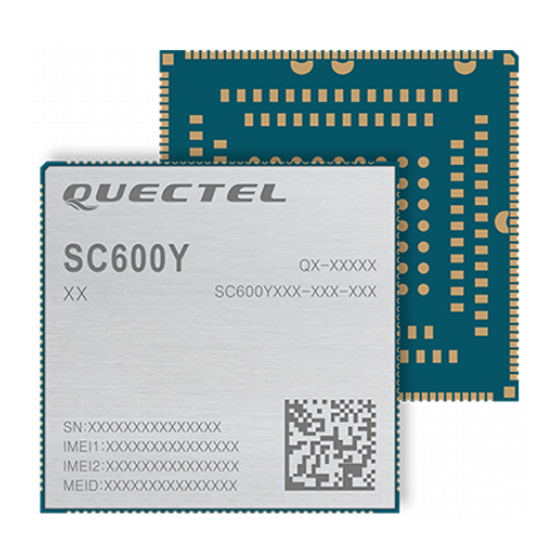
Page 122: Top And Bottom View Of The Module
Figure 47: Top View of SC600Y&SC600T Modules Figure 48: Bottom View of SC600Y&SC600T Modules NOTE These are renderings of SC600Y&SC600T modules. For authentic dimension and appearance, please refer to the module that you receive from Quectel. SC600Y&SC600T_Hardware_Design 121 / 128... - Page 123 Smart LTE Module Series SC600Y&SC600T Hardware Design Storage, Manufacturing and Packaging 9.1. Storage SC600Y&SC600T are stored in a vacuum-sealed bag. They are rated at MSL 3, and their storage restrictions are shown as below. 1. Shelf life in the vacuum-sealed bag: 12 months at <40º C/90%RH. 2.
- Page 124 Smart LTE Module Series SC600Y&SC600T Hardware Design 9.2. Manufacturing and Soldering Push the squeegee to apply the solder paste on the surface of stencil, thus making the paste fill the stencil openings and then penetrate to the PCB. The force on the squeegee should be adjusted properly so as to produce a clean stencil surface on a single pass.
- Page 125 Smart LTE Module Series SC600Y&SC600T Hardware Design Reflow Zone Max slope 2 to 3° C/sec Reflow time (D: over 220° C) 40 to 60 sec Max temperature 238° C ~ 245° C Cooling down slope 1 to 4° C/sec Reflow Cycle Max reflow cycle 9.3.
- Page 126 Smart LTE Module Series SC600Y&SC600T Hardware Design Figure 51: Reel Dimensions Table 57: Reel Packaging Model Name MOQ for MP Minimum Package: 200pcs Minimum Package×4=800pcs Size: 398mm × 383mm × 83mm Size: 420mm × 350mm × 405mm SC600Y& N.W: 1.92kg N.W: 8.18kg SC600T G.W: 3.67kg...
- Page 127 Smart LTE Module Series SC600Y&SC600T Hardware Design Appendix A References Table 58: Related Documents Document Name Remark EVB User Guide for Quectel_Smart_EVB-G2_User_Guide SC600Y&SC600T GPIO Configuration of Quectel_SC600Y&SC600T_GPIO_Configuration SC600Y&SC600T Quectel_RF_Layout_Application_Note RF Layout Application Note Quectel_Module_Secondary_SMT_User_Guide Module Secondary SMT User Guide Reference Design for Quectel_ SC600Y&SC600T_Reference_Design SC600Y&SC600T Table 59: Terms and Abbreviations...
- Page 128 Smart LTE Module Series SC600Y&SC600T Hardware Design Full Rate GMSK Gaussian Minimum Shift Keying Global Positioning System Graphics Processing Unit Global System for Mobile Communications Half Rate HSDPA High Speed Down Link Packet Access HSPA High Speed Packet Access Input/Output Inphase and Quadrature Liquid Crystal Display LCD Module...
- Page 129 Smart LTE Module Series SC600Y&SC600T Hardware Design RHCP Right Hand Circularly Polarized Real Time Clock Receive Short Message Service Terminal Equipment Transmitting Direction UART Universal Asynchronous Receiver & Transmitter UMTS Universal Mobile Telecommunications System (U)SIM (Universal) Subscriber Identity Module Vmax Maximum Voltage Value Vnorm Normal Voltage Value...
- Page 130 Smart LTE Module Series SC600Y&SC600T Hardware Design Appendix B GPRS Coding Schemes Table 60: Description of Different Coding Schemes Scheme CS-1 CS-2 CS-3 CS-4 Code Rate Pre-coded USF Radio Block excl.USF and BCS Tail Coded Bits Punctured Bits Data Rate Kb/s 9.05 13.4 15.6...
- Page 131 Smart LTE Module Series SC600Y&SC600T Hardware Design Appendix C GPRS Multi-slot Classes Twenty-nine classes of GPRS multi-slot modes are defined for MS in GPRS specification. Multi-slot classes are product dependent, and determine the maximum achievable data rates in both the uplink and downlink directions.
- Page 132 Smart LTE Module Series SC600Y&SC600T Hardware Design SC600Y&SC600T_Hardware_Design 131 / 128...
- Page 133 Smart LTE Module Series SC600Y&SC600T Hardware Design Appendix D EDGE Modulation and Coding Schemes Table 62: EDGE Modulation and Coding Schemes Coding Modulation Coding Family 1 Timeslot 2 Timeslot 4 Timeslot Schemes CS-1: GMSK 9.05kbps 18.1kbps 36.2kbps CS-2: GMSK 13.4kbps 26.8kbps 53.6kbps CS-3:...
- Page 134 Smart LTE Module Series SC600Y&SC600T Hardware Desig IC & FCC Requirement FCC Certification Requirements. According to the definition of mobile and fixed device is described in Part 2.1091(b), this device is a mobile device. And the following conditions must be met: 1.
- Page 135 Smart LTE Module Series SC600Y&SC600T Hardware Desig WIFI 2.4G/5G 5. This module must not transmit simultaneously with any other antenna or transmitter 6. The host end product must include a user manual that clearly defines operating requirements and conditions that must be observed to ensure compliance with current FCC RF exposure guidelines. For portable devices, in addition to the conditions 3 through 6 described above, a separate approval is required to satisfy the SAR requirements of FCC Part 2.1093 If the device is used for other equipment that separate approval is required for all other operating...
- Page 136 Smart LTE Module Series SC600Y&SC600T Hardware Desig The OEM integrator has to be aware not to provide information to the end user regarding how to install or remove this RF module in the user’s manual of the end product which integrates this module. The end user manual shall include all required regulatory information/warning as show in this manual.
Need help?
Do you have a question about the SC600Y-NA Series and is the answer not in the manual?
Questions and answers