
Related Manuals for ADLINK Technology Q7-AL


Summary of Contents for ADLINK Technology Q7-AL
- Page 1 Q7-AL User’s Manual Qseven Computer On Module (COM) with Embedded Intel® Atom™, Pentium®, and Celeron® Processors Manual Rev.: Revision Date: March 2, 2018 Part Number: 50-1Z231-1000...
- Page 2 Preface Copyright Copyright 2018 ADLINK Technology, Inc. This document contains proprietary information protected by copyright. All rights are reserved. No part of this manual may be reproduced by any mechanical, electronic, or other means in any form without prior written permission of the manufacturer.
-
Page 3: Table Of Contents
2.15. Operating Systems ....................19 2.16. Functional Diagram ....................20 2.17. Mechanical Drawing ....................21 2.18. Q7-AL Heatspreaders ..................... 22 2.19. Q7-AL Top View and Bottom View ................26 Pinouts and Signal Descriptions ................13 3.1. Primary/Secondary Pin Definitions ................13 3.2. -
Page 4: Preface
4.5. Status LEDs ......................33 4.6. BIOS Switch Settings ....................35 Smart Embedded Management Agent (SEMA) ............. 37 5.1. Board Specific SEMA Functions ................38 System Resources ....................41 6.1. System Memory Map ....................41 6.2. Direct Memory Access Channels ................41 6.3. -
Page 5: List Of Figures
Figure 5: Q7-AL-HS4 Passive Heatsink Mechanical Drawing ...............24 Figure 6: Q7-AL-HS5 Passive Heatsink Mechanical Drawing ...............25 Figure 7: Q7-AL Connector, Switch and LED Locations ................29 Figure 8: Q7-AL and the DB40 Debug Module ..................30 Figure 9: Q7-AL LED Locations ......................33 Figure 10: Q7-AL BIOS Switch Location ....................35... - Page 6 List of Tables Table 1: Q7-AL Primary/Secondary Pin Definitions ................13 Table 2: 36-pin MIPI-CSI Camera Connector Pin Definition on the Qseven Module......31 Table 3: 40-pin Debug Connector Pin Definition on the Qseven Module ..........32 Table 4: LED Descriptions ........................34 Table 5: BIOS Select and Mode Configuration Switch Settings.............35 Table 6: SEMA Onboard Voltage Monitor ....................38...
-
Page 7: Introduction
70mm width, 70mm length, and 2.3mm of overall height, Qseven ranks as one of the smallest COM standards currently available. The Q7-AL utilizes the upgrades in Intel’s latest (“Apollo Lake”) N-series and E-series SoCs such as the Intel 64 Architecture (“Goldmont”), the new HD graphics 500/505 engine (Gen-9), and a faster, 4-vector image processing unit. - Page 8 This page intentionally left blank. Introduction...
-
Page 9: Specifications
Q7-AL 2. Specifications 2.1. Core System Intel® Atom™ E39xx, Pentium® N4200, and Celeron® N3350, x86 dual-core or quad- core SoCs (System on Chips) with integrated memory, graphics, and I/O (formerly ‘Apollo Lake’) • Atom E3950 Quad-Core; 12W TDP; 1.6 GHz base freq; 2.0 GHz burst freq; up to 2400 MT/s;... -
Page 10: Video
2.3. Video Integrated on Processor Intel 9 Generation Low Power Graphics core architecture (Intel HD Graphics 500/505) • GPU Feature Support 2 to 3 independent and simultaneous display combinations of DisplayPort, HDMI, LVDS and eDP • Encode/transcode HD content • Playback of high definition content including Blu-ray Disc •... -
Page 11: Audio
Q7-AL 2.4. Audio Integrated Intel® HD Audio integrated on SoC Codec Located on carrier Q7-BASE (ALC886 standard support) 2.5. Integrated MAC integrated on SoC Intel PHY Intel® Ethernet Controller I210-IT or I211-IT Interface 10/100/1000 Mbit/s connection Specifications... -
Page 12: Multi I/O And Storage
All USBs supported by XHCI controller SATA 2x SATA 6Gb/s ports (1x used for optional SATA SSD) GPIO 8 GPIO from BMC multiplexed with LPC from SoC (build option) Q7-AL supports a standard USB topology as shown in the figure below: Specifications... -
Page 13: Serial I/O On Module
Q7-AL As a build option it can also be provided including a USB hub: 2.7. Serial I/O on Module Chipset: Embedded in SoC Ports: 1x UART Rx/Tx only, the bit rate can support up to 115.2k bps ... -
Page 14: Debug
2.9. Debug • 40-pin flat cable connector to be used with DB-40 debug module Supports: BIOS POST code LED, BMC access, SPI BIOS flashing, power testpoints, debug LEDs 2.10. Power Specifications Power Modes AT and ATX mode (AT mode startup controlled by SEMA Board Controller) Standard Voltage Input +5V±5% / 5Vsb ±5% Wide Voltage Input... -
Page 15: Operating Temperatures
Q7-AL Parameter 12W, E3950 9W, E3940 6W, E3930 6W, N4200 6W, N3350 Atom SoC Atom SoC Atom SoC Pentium SoC Celeron SoC System S4 0.04A (0.20W) N/A on DVT 0.04A (0.20W) N/A on DVT 0.05A (0.25W) @ mode (240 GB... -
Page 16: Functional Diagram
2.16. Functional Diagram Figure 1: Q7-AL Functional Block Diagram Specifications... -
Page 17: Mechanical Drawing
Q7-AL 2.17. Mechanical Drawing All are dimensions shown in millimeters. Tolerances should be ± 0.25mm, unless otherwise noted. Figure 2: Q7-AL Mechanical Drawing Specifications... -
Page 18: Q7-Al Heatspreaders
2.18. Q7-AL Heatspreaders The Q7-AL is designed to operate at its maximum CPU speed and requires a thermal solution to cool the CPU. ADLINK offers two passive heatsinks, one active heatsink, and two heat spreaders for cooling. Each Q7-AL module... -
Page 19: Figure 4: Q7-Al-Hs2 Heat Spreader Mechanical Drawing
Q7-AL 2.18.2. The Q7-AL-HS2 heat spreader is designed for the Q7-AL-N4200/N3350 modules and must be used for these lower profile SoCs. As can be seen in Figure-1, the Intel Pentium and Celeron N4200/N3350 SoCs come without mounted Intel heat spreaders, and their profiles are 2mm lower than the Atom E39xx SoCs. -
Page 20: Figure 5: Q7-Al-Hs4 Passive Heatsink Mechanical Drawing
Figure-1, the Intel Atom E39xx SoCs come with mounted Intel heat spreaders, which look like metallic lids and add 2mm to the heights of the SoCs. The Q7-AL-HS-4 passive heatsink is designed for the extra heights of these SoCs. See the following diagram for a mechanical overview of the Q7-AL-HS-4 passive heatsink. -
Page 21: Figure 6: Q7-Al-Hs5 Passive Heatsink Mechanical Drawing
Q7-AL 2.18.4. The Q7-AL-HS-5 passive heatsink is designed for the Q7-AL-N4200/N3350 modules and must be used for these lower profile SoCs. As can be seen in Figure-1, the Intel Pentium and Celeron N4200/N3350 SoCs come without mounted Intel heat spreaders, and their profiles are 2mm lower than the Atom E39xx SoCs. -
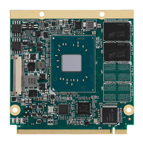
Page 22: Q7-Al Top View And Bottom View
2.19. Q7-AL Top View and Bottom View Specifications... -
Page 23: Pinouts And Signal Descriptions
Primary/Secondary Pin Definitions The Q7-AL is a Qseven 2.1 compliant module supporting some of the options of the specification. All pins in the Qseven 2.1 specification are described, including those not supported on the Q7-AL. Those not supported on the Q7-AL module are crossed out. - Page 24 Primary side (BOTTOM) Secondary side (TOP) Reserved USB_OTG_VBUS HDA_SYNC /I2S_WS SMB_CLK /GP1_I2C_CLK HDA_RST# SMB_DAT /I2S_RST# /GP1_I2C_DAT HDA_BITCLK SMB_ALERT# /I2S_CLK HDA_SDI GP0_I2C_CLK /I2S_SDI HDA_SDO GP0_I2C_DAT /I2S_SDO THRM# WDTRIG# THRMTRIP# WDOUT U3_USB1_TX_N U3_USB1_RX_N USB_P7- USB_P6- /USB_SSTX0- /USB_SSRX0- U3_USB1_TX_P U3_USB1_RX_P USB_P7+/USB_SST USB_P6+/USB_SSR USB_OC1# USB_OC1# USB_6_7_OC# USB_4_5_OC#...
- Page 25 Q7-AL Primary side (BOTTOM) Secondary side (TOP) [LVDS Default] [LVDS Default] eDP0_TX1+ / PU, 470k, V1P8S DDI0_TX1+ LVDS_A1+ eDP1_TX1+ / [LVDS Default] LVDS_B1+ [LVDS Default] eDP0_TX1- / PU, 470k, V1P8S DDI0_TX1- LVDS_A1- eDP1_TX1- / [LVDS Default] LVDS_B1- [LVDS Default] eDP0_TX2+ /...
- Page 26 Primary side (BOTTOM) Secondary side (TOP) DP_LANE1+ / DP_AUX+ TMDS_LANE1+ DP_LANE1- / DP_AUX- TMDS_LANE1- DP_LANE2+ / U3_USB0_RX_N TMDS_LANE0+ USB_SSRX1- DP_LANE2- / U3_USB0_RX_P TMDS_LANE0- USB_SSRX1+ DP_LANE0+ / HDMI_CTRL_DAT TMDS_LANE2+ DP_LANE0- / HDMI_CTRL_CLK TMDS_LANE2- DP_HDMI_HPD# DP_HPD# PCIE_CLK_REF+ PCIE_WAKE# PCIE_CLK_REF- PCIE_RST# PCIE3_TX+ PCIE3_RX+ PCIE3_TX- PCIE3_RX- PCIE2_TX+...
- Page 27 Q7-AL Primary side (BOTTOM) Secondary side (TOP) SPI_MISO SPI_CS1# SPI_SCK MFG_NC4 VCC_5V_SB VCC_5V_SB MFG_NC0 MFG_NC2 MFG_NC1 MFG_NC3 Notes: (1) eDP is available as a build option in place of LVDS. Pinouts and Signal Descriptions...
-
Page 28: Signal Description Terminology
3.2. Signal Description Terminology The following terms are used in the Qseven Signal Descriptions below. Input to the Module Output from the Module Bi-directional input/output signal Open drain output I 3.3V Input 3.3V tolerant I 5V Input 5V tolerant O 3.3V Output 3.3V signal level O 5V Output 5V signal level... -
Page 29: Qseven Signal Descriptions
Q7-AL 3.3. Qseven Signal Descriptions 3.3.1. Gigabit Ethernet Gigabit Ethernet Description PU/PD Comment Media Dependent Interface (MDI) differential pair 0. The GBE0_MDI0+ Twisted pair MDI can operate in 1000, 100, and 10Mbit/sec modes. GBE0_MDI0- Gb_LAN signals for external This signal pair is used for all modes. - Page 30 3.3.3. SDIO Signal Description PU/PD Comment SDIO_CD# SDIO Card Detect. This signal indicates when an SDIO/MMC card is present. CMOS 100K 3.3V 3.3V SDIO_CLK SDIO Clock. With each cycle of this signal a one-bit transfer on the command and each data line occurs. CMOS 3.3V SDIO_CMD...
- Page 31 Q7-AL 3.3.5. Miscellaneous Signal Description PU/PD Comment WDTRIG# Watchdog trigger signal. This signal restarts the watchdog timer of the Qseven ® module CMOS 3.3V on the falling edge of a low active pulse. WDOUT Watchdog event indicator. High active output used for signaling a missing CMOS 3.3V...
- Page 32 Signal Description PU/PD Comment PU 2.2K 3.3V GPO0 General Purpose Output 0 CMOS 3.3V 3.3.6. Signal Description PU/PD Comment U2_USB1_P USB 2.0 differential data pairs for Port 1 USB 1.1/ 2.0 compliant U2_USB1_N 3.3VSB U2_USB2_P USB 2.0 differential data pairs for Port 2 USB 1.1/ 2.0 compliant U2_USB2_N 3.3VSB...
- Page 33 Q7-AL 3.3.7. LVDS Signal Description PU/PD Comment LVDS_A0+ LVDS Channel A differential pairs LVDS is default LVDS_A0- LVDS (through eDP to LVDS_A1+ LVDS bridge) LVDS_A1- LVDS_A2+ Note: eDP support LVDS_A2- LVDS_A3+ is a build option LVDS_A3- LVDS_A_CK+ LVDS Channel A differential clock...
- Page 34 3.3.9. DisplayPort Signal Description PU/PD Comment DP_LANE3+ DDI1 differential pair for DisplayPort AC coupled on lane 3 module DP_LANE3- eDP/DP DP_LANE1+ DDI1 differential pair for DisplayPort AC coupled on lane 1 module DP_LANE1- eDP/DP DP_LANE2+ DDI1 differential pair for DisplayPort AC coupled on lane 2 module...
- Page 35 Q7-AL 3.3.11. PCI Express Signal Description PU/PD Comment PCIE0_TX+ PCI Express channel 0, Transmit Output AC coupled on module PCIE0_TX- differential pair. PCIE PCIE0_RX+ PCI Express channel 0, Receive Input AC coupled close to PCIE0_RX- differential pair. PCIE respective device...
- Page 36 3.3.13. LPC Bus Signal Description PU/PD Comment LPC_AD0 LPC multiplexed address, command, and data bus signal 0 CMOS 3.3V LPC_AD1 LPC multiplexed address, command, and data bus signal 1 CMOS 3.3V LPC_AD2 LPC multiplexed address, command, and data bus signal 2 CMOS 3.3V LPC_AD3...
- Page 37 Q7-AL 3.3.15. Power and System Management Signal Description PU/PD Comment PWRBTN# Power Button: Low active power button input. This signal is PU 100K triggered on the falling edge. CMOS 3.3V 3.3V suspend S3 State: This signal shuts off power to all runtime system...
- Page 38 3.3.17. Thermal Management Signal Description PU/PD Comment THRM# Thermal Alarm active low signal generated by the external hardware to indicate an over CMOS temperature situation. This signal can be 3.3V used to initiate thermal throttling. THERMTRIP# Thermal Trip indicates an overheating condition of the processor.
-
Page 39: Connector Pinouts On Module
This chapter describes connectors, LEDs, and switches that are used on the module. 4.1. Connector, Switch, and LED Locations Figure 7: Q7-AL Connector, Switch and LED Locations 4.2. Q7-AL and the DB40 Debug Module The DB40 debug board can be connected via a FPC 40-pin flat cable to the module. It provides bus extensions to the SPI bus (out of band BIOS flashing) and the BMC (access to Board Management Controller). -
Page 40: 36-Pin Mipi-Csi2 Camera Connector
Figure 8: Q7-AL and the DB40 Debug Module 4.3. 36-pin MIPI-CSI2 Camera Connector FPC Connector Type: Flatfoil with 0.5mm pitch Pin Orientation Connector Pinouts on Module... -
Page 41: Table 2: 36-Pin Mipi-Csi Camera Connector Pin Definition On The Qseven Module
Q7-AL Table 2: 36-pin MIPI-CSI Camera Connector Pin Definition on the Qseven Module Signal Description V3P3S 3.3 volts +/-5% to power the camera device (output) V3P3S 3.3 volts +/-5% to power the camera device (output) MCSI1_D0_P CSI1 Camera 0 Data Lane 0+... -
Page 42: 40-Pin Debug Connector
4.4. 40-pin Debug Connector FPC Connector Type: FCI 59GF Flex 10042867 Pin Orientation Table 3: 40-pin Debug Connector Pin Definition on the Qseven Module Interface Signal RESERVED SMC_STATUS BIOS_MODE SMC Debug SEL_BIOS POSTWDT_DIS# SUS_S5# SUS_S4# SUS_S3# Test Point CB_PWROK CB_RESET# SYS_RESET# PWRBTN# SMC_OCD0B... -
Page 43: Status Leds
Note: The pin definition on the debug module is the inverse of that on the Qseven module. 4.5. Status LEDs To facilitate easier maintenance, status LEDs are mounted on the board. Figure 9: Q7-AL LED Locations Connector Pinouts on Module... -
Page 44: Table 4: Led Descriptions
Table 4: LED Descriptions Name Color Connection Function LED1 Blue BMC output Power Sequence Status Code (BMC) Power Changes, RESET (see 5.1.4 Exception Codes below) During startup of the module this LED may be lit or show blink codes. During normal operation, this LED is switched off. LED2 Green Power Source 3Vcc... -
Page 45: Bios Switch Settings
Q7-AL 4.6. BIOS Switch Settings Figure 10: Q7-AL BIOS Switch Location BIOS Select and Mode Configuration Switch The module has two BIOS chips, and BIOS operation can be configured to "Normal" and dual-BIOS "Failsafe" modes using the BIOS Select and Mode Configuration switch (BSW1), Pin 2. - Page 46 This page intentionally left blank. Connector Pinouts on Module...
-
Page 47: Smart Embedded Management Agent (Sema)
Q7-AL 5. Smart Embedded Management Agent (SEMA) The onboard microcontroller (BMC) implements power sequencing and Smart Embedded Management Agent (SEMA) functionality. The microcontroller communicates via the System Management Bus with the CPU/chipset. The following functions are implemented: ‧ Total operating hours counter. Counts the number of hours the module has been run in minutes. -
Page 48: Board Specific Sema Functions
5.1.2. Main Current The BMC of the Q7-AL implements a current monitor. The current can be read by calling the SEMA function “Get Main Current”. The function returns four 16-bit values divided in high-byte (MSB) and low-byte (LSB). These 4 values represent the last 4 currents drawn by the board. -
Page 49: Table 8: Sema Exception Codes
Q7-AL 5.1.4. Exception Codes In case of an error, the BMC drives a blinking code on the blue Status LED (LED1). The same error code is also reported by the BMC Flags register. The Exception Code is not stored in the Flash Storage and is cleared when the power is removed. - Page 50 This page intentionally left blank. Smart Embedded Management Agent (SEMA)
-
Page 51: System Resources
Q7-AL 6. System Resources 6.1. System Memory Map Address Range (decimal) Address Range (hex) Size Description (4GB-2MB) FFE00000 – FFFFFFFF 16 MB High BIOS Area (4GB-18MB) – (4GB-17MB-1) FEE00000 – FEEFFFFF 1 MB MSI Interrupts (4GB-20MB) – (4GB-19MB-1) FEC00000 – FECFFFFF... - Page 52 Hex Range Device 52h – 53h Timer/Counter LPC/eSPI NMI Controller Microcontroller NMI Controller1 Microcontroller NMI Controller1 Microcontroller NMI Controller1 RTC Controller RTC Controller RTC Controller RTC Controller RTC Controller RTC Controller 76h – 77h RTC Controller LPC/eSPI or PCIe 84h – 86h Reserved Reserved 8Ch –...
-
Page 53: Interrupt Request (Irq) Lines
Q7-AL 6.4. Interrupt Request (IRQ) Lines PIC Mode IRQ# Typical Interrupt Resource Connected to Pin Available Counter 0 Keyboard controller Cascade interrupt from slave PIC Serial Port 3 (COM3) Note (1) Serial Port 2 (COM2) Note (1) Serial Port 1 (COM1) -
Page 54: Pci Configuration Space Map
IRQ# Typical Interrupt Resource Connected to Pin Available Secondary IDE controller IRQ15 via SERIRQ / PIRQ Note (1) P.E.G Root Port, Intel HDA, PCIE Port Note (1) 0/1/2/3/4/5/6, EHCI Controller #2 , I.G.D ,XHCI Controller PCIE Port 0/1/2/3/4/5/6, P.E.G Root Note (1) Port, PCIE Port 0/1/2/3/4/5/6, P.E.G Root... - Page 55 Q7-AL Device: Functions # Function Description Bus 0: Device 28: Function 3 PCI Express Port 4 Bus 0: Device 28: Function 4 PCI Express Port 5 Bus 0: Device 28: Function 5 PCI Express Port 6 Bus 0: Device 28: Function 6...
-
Page 56: Pci Interrupt Routing Map
6.6. PCI Interrupt Routing Map P.E.G. Root Audio xHCI Controller ME Controller ME Controller IDE-R Line Port Controller Int0 INTA:16 INTA:16 INTA:16 INTA:16 Int1 INTB:17 INTD:17 Int2 INTC:18 INTC:18 Int3 INTD:19 INTB:19 PCIE port1 PCIE port 2 PCIE port 3 PCIE port 4 PCIE port5 Line... -
Page 57: Bios Setup
Q7-AL 7. BIOS Setup 7.1. Menu Structure This section presents the six primary menus of the BIOS Setup Utility. Use the following table as a quick reference for the contents of the BIOS Setup Utility. The subsections in this section describe the submenus and setting options for each menu item. -
Page 58: Main
7.2. Main The Main Menu provides read-only information about your system and also allows you to set the System Date and Time. Refer to the following tables for details of the submenus and settings. 7.2.1. BIOS Information Feature Options Description BIOS Vendor Info only Vendor... - Page 59 Q7-AL 7.2.3. Board Information 7.2.3.1. Board Information > Board Information Feature Options Description Serial Number Info only Display System Serial Number Manufacturing Date Read only Display Manufacturing Date Last Repair Date Read only Display Last Repair Date MAC ID Read only Display MAC ID 7.2.3.2.
-
Page 60: Advanced
7.3. Advanced This menu contains the settings for most of the user interfaces in the system. 7.3.1. Advanced > CPU Configuration Feature Options Description CPU Configuration Info only ► Submenu Display socket specific CPU Information Socket 0 CPU Information Speed Info only Display CPU Speed Frequency 64-bit... - Page 61 Q7-AL Feature Options Description L2 Cache Info only Display L2 Cache L3 Cache Info only Display L3 Cache 7.3.1.2. Advanced > CPU Configuration > CPU Power Management Feature Options Description CPU Power Management Info only Configuration EIST Disabled Enable/Disable Intel SpeedStep...
- Page 62 Feature Options Description Power Limit 1 Time Window Auto Power Limit 1 Time Window value in Seconds. Auto will program Power Limit 1 Time Window based on silicon default support value. 7.3.2. Advanced > Graphics Configuration Feature Options Description LVDS Info only Data format and Color Depth VESA 24 bpp...
- Page 63 Q7-AL Feature Options Description Active Low LVDS Backlight Brightness Value Range A change takes effect immediately. The Value range starts by 0 and ends of 255. 7.3.3. Advanced > Power Management Feature Options Description Enable ACPI Auto Configuration Disabled Enable/Disable BIOS ACPI Auto Configuration.
- Page 64 7.3.4. Advanced > System Management Feature Options Description System Management Info only Version Info only Display Version SEMA Firmware Read only Display SEMA firmware Build Date Read only Display SEMA firmware build date SEMA Boot loader Read only Display SEMA boot loader Build Date Read only Display SEMA boot loader build date...
- Page 65 Q7-AL 7.3.4.2. Advanced > System Management > Flags Feature Options Description Flags Info only BMC Flags Read only BIOS Select Read only Display the selection of current BIOS ROM. ATX/AT-Mode Read only Display ATX/AT-Mode. Exception Code Read only System exception reason.
- Page 66 7.3.6. Advanced > Watchdog Timer Feature Options Description Watchdog Timer Info only RunTime Watchdog Disabled The Runtime Watchdog resets the system after a certain amount of time after power up Enabled 7.3.7. Advanced > CSM Configuration Feature Options Description Compatibility Support Module Info only Configuration CSM Support...
- Page 67 Q7-AL 7.3.8. Advanced > Super IO Configuration Feature Options Description W83627DHG Info only ► Submenu Set Parameters of serial port 1 Serial Port1 Configuration Serial Port 1 Configuration Info only Serial Port Disabled Enable or Disable Serial Port (COM) Enabled...
- Page 68 Feature Options Description Bits per second 9600 Selects serial port transmission speed. The speed must be matched on the remote computer. Long or 19200 noisy lines may require lower speeds. 38400 57600 115200 Data Bits Select data bits. None Parity Select parity.
- Page 69 Q7-AL Feature Options Description Device reset time-out 10 sec USB mass storage device start unit command time- out. 20 sec 30 sec 40 sec Device power-up delay Auto Maximum time the device will take before it properly reports itself to the host controller.
-
Page 70: Chipset
7.4. Chipset Feature Options Description North Bridge ► Submenu North Bridge Parameters South Bridge ► Submenu South Bridge Parameters Uncore Configuration ► Submenu Uncore Configuration. South Cluster Configuration ► Submenu South Cluster Configuration 7.4.1. Chipset > North Bridge Feature Options Description Memory Information Info Only... - Page 71 Q7-AL 7.4.3. Chipset > Uncore Configuration 7.4.3.1. Chipset > Uncore Configuration > GOP Configuration Feature Options Description No LFP Active LFP Config Active Local Flat Panel Config GTT Mode LVDS Backlight Mode Select LVDS Backlight control function. BMC Mode DDI Port 2...
- Page 72 Feature Options Description 320MB 352MB 384MB 416MB 448MB 480MB 512MB DVMT Total Gfx Mem 128M Select DVMT5.0 Total Graphic Memory size used by the Internal Graphics Device. 256M 7.4.4. Chipset > South Cluster Configuration Feature Options Description HD-Audio Configuration ► Submenu HD-Audio Configuration Settings PCI Express Configuration ►...
- Page 73 Q7-AL Feature Options Description Enable: Enable PCIE root port Disable: Disable PCIE root port ► Submenu Control the PCI Express Root Port. PCIe Express Root Port2 Auto: To disable unused root port automatically for the most optimum power savings. Enable: Enable PCIE root port Disable: Disable PCIE root port ►...
- Page 74 Feature Options Description SEFE Disabled Root PCI Express System Error on Fatal Error Enable/Disable. Enabled SENFE Disabled Enable or disable Root PCI Express System Error on Non-Fatal Error. Enabled SECE Disabled Root PCI Express System Error on Correctable Error Enable/Disable. Enabled PME SCI Disabled...
- Page 75 Q7-AL Feature Options Description SATA Mode Selection AHCI Determines how SATA Controller(s) operate. SATA Interface Speed Gen1 Select SATA Interface Speed, CHV A1 always with Gen1 Speed Gen2 Gen3 SATA Test Mode Disabled Test mode Enabled / Disabled Enabled Disabled Aggressive LPM Support Enable PCH to aggressively enter link power state.
-
Page 76: Security
7.4.4.5. Chipset > South Cluster Configuration > USB Configuration Feature Options Description XHCI Pre-Boot Driver Disabled Enable/Disable XHCI Pre-Boot Driver Support Enabled XHCI Mode Disabled Once disable, XHCI controller would be function disabled, none of the USB devices are detectable and Enabled usable during boot and in OS. -
Page 77: Boot
Q7-AL 7.6. Boot 7.6.1. Boot > Boot Configuration Feature Options Description Boot Configuration Info only Setup Prompt Timeout Number of seconds to wait for setup activation key. 65535 (0xFFFF ) means indefinite waiting. Bootup NumLock State Select the keyboard NumLock state. - Page 78 This page intentionally left blank. BIOS Setup...
-
Page 79: Bios Checkpoints, Beep Codes
Q7-AL 8. BIOS Checkpoints, Beep Codes This section lists checkpoints and beep codes generated by the AMI Aptio BIOS. The checkpoints defined in this document are inherent to the AMIBIOS generic core and do not include any chipset or board specific checkpoint definitions. -
Page 80: Status Code Ranges
8.1. Status Code Ranges Status Code Description Range 0x01 – 0x0B SEC execution 0x0C – 0x0F SEC errors 0x10 – 0x2F PEI execution up to and including memory detection 0x30 – 0x4F PEI execution after memory detection 0x50 – 0x5F PEI errors 0x60 –... - Page 81 Q7-AL SEC Error Codes 0x0C – 0x0D Reserved for future AMI SEC error codes 0x0E Microcode not found 0x0F Microcode not loaded 8.2.2. SEC Beep Codes None 8.2.3. PEI Phase Status Code Description Progress Codes 0x10 PEI Core is started...
- Page 82 Status Code Description 0x35 CPU post-memory initialization. Boot Strap Processor (BSP) selection 0x36 CPU post-memory initialization. System Management Mode (SMM) initialization 0x37 Post-Memory North Bridge initialization is started 0x38 Post-Memory North Bridge initialization (North Bridge module specific) 0x39 Post-Memory North Bridge initialization (North Bridge module specific) 0x3A Post-Memory North Bridge initialization (North Bridge module specific) 0x3B...
- Page 83 Q7-AL Status Code Description S3 Resume Error Codes 0xE8 S3 Resume Failed 0xE9 S3 Resume PPI not Found 0xEA S3 Resume Boot Script Error 0xEB S3 OS Wake Error 0xEC-0xEF Reserved for future AMI error codes Recovery Progress Codes 0xF0...
- Page 84 8.2.5. DXE Status Codes Status Code Description 0x60 DXE Core is started 0x61 NVRAM initialization 0x62 Installation of the South Bridge Runtime Services 0x63 CPU DXE initialization is started 0x64 CPU DXE initialization (CPU module specific) 0x65 CPU DXE initialization (CPU module specific) 0x66 CPU DXE initialization (CPU module specific) 0x67...
- Page 85 Q7-AL Status Code Description 0x95 PCI Bus Request Resources 0x96 PCI Bus Assign Resources 0x97 Console Output devices connect 0x98 Console Input devices connect 0x99 Super IO Initialization 0x9A USB initialization is started 0x9B USB Reset 0x9C USB Detect 0x9D USB Enable 0x9E –...
- Page 86 Status Code Description 0xB8 – 0xBF Reserved for future AMI codes 0xC0 – 0xCF OEM BDS initialization codes DXE Error Codes 0xD0 CPU initialization error 0xD1 North Bridge initialization error 0xD2 South Bridge initialization error 0xD3 Some of the Architectural Protocols are not available 0xD4 PCI resource allocation error.
-
Page 87: Oem-Reserved Checkpoint Ranges
Q7-AL Status Code Description 0x10 System is waking up from the S1 sleep state 0x20 System is waking up from the S2 sleep state 0x30 System is waking up from the S3 sleep state 0x40 System is waking up from the S4 sleep state 0xAC System has transitioned into ACPI mode. - Page 88 This page intentionally left blank. BIOS Checkpoints, Beep Codes...
-
Page 89: Mechanical Information
Q7-AL 9. Mechanical Information 9.1. Board-to-Board Connector The high-speed serialized Qseven edge connector is designed for ultra-low power CPUs and chipsets with ultra- low Thermal Design Power (TDP). Refer to the following illustration for the mechanical dimensions of the Qseven edge connector. -
Page 90: Thermal Solution
9.2. Thermal Solution 9.2.1. Heat Spreaders The function of the heat spreader is to ensure an identical mechanical profile for all Qseven modules. By using a heat spreader, the thermal solution that is built on top of the module is compatible with all Qseven modules. 9.2.2. - Page 91 Q7-AL Step 4: Lay the heat spreader or heatsink on the module so that the thermal pads on the heat spreader or heatsink completely cover their respective components on the module, and the mounting holes on the heat spreader or heatsink line up with the mounting holes on the module.
- Page 92 Step 4: Use the four 2.7mm countersink screws provided to fasten the heat spreader or four 2.7mm panhead screws to fasten the passive heatsink to the module. Refer to the following four photos. Install the screws using an alternating installation sequence as the red arrows in the second two photos indicate. Mechanical Information...
-
Page 93: Mounting Requirements
Q7-AL 9.3. Mounting Requirements Qseven modules accommodate Top mounting to the carrier board. In Top mounting, the threaded standoffs are on the carrier board and the thermal solution is equipped with through-hole standoffs. For mounting dimension requirements, refer to the following diagram from the Qseven 2.0 specification. -
Page 94: Safety Instructions
Safety Instructions Read and follow all instructions marked on the product and in the documentation before you operate your system. Retain all safety and operating instructions for future use. • Please read these safety instructions carefully. • Please keep this User‘s Manual for later reference. •... -
Page 95: Getting Service
5215 Hellyer Avenue, #110, San Jose, CA 95138, USA Tel: +1-408-360-0200 Toll Free: +1-800-966-5200 (USA only) Fax: +1-408-360-0222 Email: info@adlinktech.com ADLINK Technology (China) Co., Ltd. Address: 300 Fang Chun Rd., Zhangjiang Hi-Tech Park, Pudong New Area Shanghai, 201203 China Tel: +86-21-5132-8988 Fax: +86-21-5132-3588 Email: market@adlinktech.com...
Need help?
Do you have a question about the Q7-AL and is the answer not in the manual?
Questions and answers