
Related Manuals for ADLINK Technology nanoX-EL


Summary of Contents for ADLINK Technology nanoX-EL
- Page 1 User’s Guide PICMG COM.0 R3.0 nanoX-EL User’s Guide Revision: Rev. 0.1 Preliminary Date: 2021-11-11 Part Number: 50M-00055-1000 Page 1 Copyright © 2021 ADLINK Technology, Inc.
-
Page 2: Preface
Product names mentioned herein are used for identification purposes only and may be trademarks / registered trademarks of respective companies. Copyright © 2021 ADLINK Technology Incorporated This document contains proprietary information protected by copyright. All rights are reserved. No part of this manual may be reproduced by any mechanical, electronic, or other means in any form without prior written permission of the manufacturer. - Page 3 Only install/attach and operate equipment on stable surfaces and/or recommended mountings; If the equipment will not be used for long periods of time, turn off the power source and unplug the equipment. Page 3 Copyright © 2021 ADLINK Technology, Inc.
- Page 4 Caution: This information indicates the possibility of minor physical injury, component damage, data loss, and/or program corruption. Warning: This information warns of possible serious physical injury, component damage, data loss, and/or program corruption. Page 4 Copyright © 2021 ADLINK Technology, Inc.
- Page 5 User’s Guide PICMG COM.0 R3.0 Revision History Revision Description Date Author Preliminary release 2021-11-11 Page 5 Copyright © 2021 ADLINK Technology, Inc.
-
Page 6: Table Of Contents
DDI0 Port ..................................................................28 4.3.4 Gigabit Ethernet................................................................. 31 4.3.5 SATA ....................................................................32 4.3.6 PCI Express ................................................................... 33 4.3.7 LPC Bus ..................................................................35 4.3.8 USB 2.0/1.1................................................................... 36 4.3.9 USB 3.x Extension ..............................................................37 Page 6 Copyright © 2021 ADLINK Technology, Inc. - Page 7 8.2. Thermal Solutions ................................................................. 53 8.2.1 Heatspreader – Bottom Mount: HTS-nXEL-B-I ..................................................... 53 8.2.2 Heatsink High Profile – Bottom Mount: THSH-nXEL-B-I ................................................54 8.2.3 Heatsink Low Profile – Bottom Mount: THS-nXEL-B-I ................................................55 Page 7 Copyright © 2021 ADLINK Technology, Inc.
-
Page 8: List Of Figures
Figure 2 - Module rear side row and pin numbering ..............................................18 Figure 3 – Module feature locations ....................................................... 45 Figure 4 – nanoX-EL and Debug Module ..................................................... 46 Figure 5 – Module mechanical dimensions ..................................................52 Figure 6 – Heatspreader – Bottom Mount: HTS-nXEL-B-I .............................................. 53 Figure 8 –... -
Page 9: Introduction
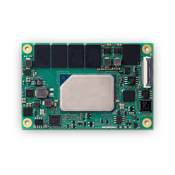
Warning: this is an EA (early available) engineering manual, meaning contents may not properly reflect the actual or final version of this product The nanoX-EL is the first COM Express® COM.0 R3.0 Mini Size Type 10 module featuring the IT/OT convergence 6th Generation Intel Atom® x6000E processor and Pentium, Celeron processors (formerly “Elkhart Lake”). -
Page 10: Specifications
SKUs with Intel® TCC feature paired with specific LAN solutions can support TSN (TBC). Pentium, Celeron and some of Atom SKUs are supported by project basis. Please contact your local ADLINK presentative. Page 10 Copyright © 2021 ADLINK Technology, Inc. -
Page 11: Video
Playback of HD content, including Blu-ray Disc and Blu-ray Disc 3D, using HDMI (1.4a spec compliant with 3D) Intel® QuickSync and Intel® Clear Video HD HEVC/H.265 10-bit/8-bit, H.264, M/JPEG, MPEG2, VC1/WMV9, VP9, VP8 HW decode Page 11 Copyright © 2021 ADLINK Technology, Inc. -
Page 12: Display Interface Support
4 PCI Express x1 Gen3: Lanes 0,1,2,3 (configurable to 4 x1, 2 x2, 1 x4, 2 x1 + 1 x2, 1 x2 + 2 x1) Other: SMBus (system), I2C (user), LPC bus (via eSPI-to-LPC bridge IC) Page 12 Copyright © 2021 ADLINK Technology, Inc. -
Page 13: Ethernet
COM 3 Supported by Super I/O (W83627DHG) on carrier board 0x240 COM 4 Supported by Super I/O (W83627DHG) on carrier board 0x248 Note: SER0, SER1 from SoC HSUART are BOM option support by project basis Page 13 Copyright © 2021 ADLINK Technology, Inc. - Page 14 VxWorks Enterprise (Yotco) (Ubuntu) OS Installation eMMC Note: eMMC and SD functionality as an OS installation device may change dependent on Intel updates. Please contact your local sales representative for more information. Page 14 Copyright © 2021 ADLINK Technology, Inc.
-
Page 15: Trusted Platform Module (Tpm)
Power Management: ACPI 5.0 compliant, Smart Battery support Power States: C1-C6, S0, S1, S3, S4, S5, S5 ECO mode (Wake-on-USB S3/S4, WoL S3/S4/S5) ECO Mode support for deep S5 for 5Vsb power saving Page 15 Copyright © 2021 ADLINK Technology, Inc. -
Page 16: Mechanical And Environmental
Shock and Vibration IEC 60068-2-64 and IEC-60068-2-27 MIL-STD-202F, Method 213B, Table 213-I, Condition A and Method 214A, Table 214-I, Condition D HALT tested Thermal Stress, Vibration Stress, Thermal Shock and Combined Test Page 16 Copyright © 2021 ADLINK Technology, Inc. -
Page 17: Block Diagram
BIOS SMBus SDIO 3.0 HSUART eSPI Thermal sensor eMMC 5.1 GPIO/SDIO (SOC) 16GB-64GB Embedded Controller Thermal UART 0-1/CAN sensor build option (board) LPC/eSPI eSPI to LPC Figure 1 – Module function diagram Page 17 Copyright © 2021 ADLINK Technology, Inc. -
Page 18: Pinout And Signal Descriptions
The table below is a comprehensive list of all signal pins supported on the single 220-pin COM Express connectors as defined for Type 10 in the PICMG COM.0 R3.0 specification. Signals described in the specification but not supported on the nanoX-EL are strikethrough STRIKETHROUGH. - Page 19 GND (FIXED) GND (FIXED) USB_SSRX0- USB_SSTX0- USB_SSRX0+ USB_SSTX0+ SUS_S5# PWR_OK USB_SSRX1- USB_SSTX1- USB_SSRX1+ USB_SSTX1+ BATLOW# (S)ATA_ACT# AC/HDA_SDIN2 HDA_SYNC AC/HDA_SDIN1 HDA_RST# AC/HDA_SDIN0 GND (FIXED) GND (FIXED) HDA_BITCLK SPKR HDA_SDOUT I2C_CK BIOS_DIS0#/ESPI_SAFS I2C_DAT THRMTRIP# THRM# Page 19 Copyright © 2021 ADLINK Technology, Inc.
- Page 20 RSVD RSVD- GPO2 PCIE_TX3+ PCIE_RX3+ PCIE_TX3- PCIE_RX3- GND (FIXED) GND (FIXED) PCIE_TX2+ PCIE_RX2+ PCIE_TX2- PCIE_RX2- GPI1 GPO3 PCIE_TX1+ PCIE_RX1+ PCIE_TX1- PCIE_RX1- WAKE0# GPI2 WAKE1# PCIE_TX0+ PCIE_RX0+ PCIE_TX0- PCIE_RX0- GND (FIXED) GND (FIXED) Page 20 Copyright © 2021 ADLINK Technology, Inc.
- Page 21 TYPE10# SPI_CS# SER0_TX DDI0_CTRLCLK_AUX+ SER0_RX DDI0_CTRLDATA_AUX- A100 GND (FIXED) B100 GND (FIXED) A101 SER1_TX/CAN_TX B101 FAN_PWMOUT A102 SER1_RX/CAN_RX B102 FAN_TACHIN A103 LID# B103 SLEEP# A104 VCC_12V B104 VCC_12V A105 VCC_12V B105 VCC_12V Page 21 Copyright © 2021 ADLINK Technology, Inc.
- Page 22 Note: STRIKETHROUGH strike-through entries are not supported functions on this product eDP (in place of LVDS) is BOM option support by project basis SD (in place of GPIO) is BOM option support by project basis Page 22 Copyright © 2021 ADLINK Technology, Inc.
-
Page 23: Signal Terminology Descriptions
Pull-down strap. A Module output pin that is either tied to GND or is not connected. Used to signal Module capabilities to the Carrier Board. PU (pull-up) resistor on module PD (pull-down) resistor on module Page 23 Copyright © 2021 ADLINK Technology, Inc. -
Page 24: Ab Connector Signal Descriptions
Serial TDM data output to the CODEC. O 3.3V HDA_SDOUT AC_SDIN[2:0] / B28- B30 Serial TDM data inputs from up to 3 CODECs. B28 (SDIN2) Not supported HDA_SDIN[2:0] 3.3VSB Elkhart Lake doesn’t offer this pin Page 24 Copyright © 2021 ADLINK Technology, Inc. -
Page 25: Lvds Or Edp
LVDS_A2+ eDP_TX0+ LVDS_A2- eDP_TX0- LVDS_A3+ LVDS_A3- LVDS_A_CK+ eDP_TX3+ LVDS_A_CK- eDP_TX3- LVDS_VDD_EN eDP_VDD_EN LVDS_BKLT_EN eDP_BKLT_EN LVDS_BKLT_CTRL eDP_BKLT_CTRL LVDS_I2C_CK eDP_AUX+ LVDS_I2C_DAT eDP_AUX- eDP_HPD Note: LVDS is default, eDP is BOM option by project basis Page 25 Copyright © 2021 ADLINK Technology, Inc. - Page 26 PD 100K LVDS_I2C_CK DDC lines used for flat panel detection and control. O 3.3V PU 2k2 3.3V LVDS_I2C_DAT DDC lines used for flat panel detection and control. I/O 3.3V PU 2k2 3.3V Page 26 Copyright © 2021 ADLINK Technology, Inc.
- Page 27 I/O PCIE AC coupled off module eDP_HPD Detection of Hot Plug / Unplug and notification of the I 3.3V PD 100K PD 100K on this pin when eDP is supported link layer Page 27 Copyright © 2021 ADLINK Technology, Inc.
-
Page 28: Ddi0 Port
DP_AUX+ /- pair must be AC coupled. A set of FET switches may be used to resolve this problem. The FET gates can be controlled by the AUX_SEL pin function. Page 28 Copyright © 2021 ADLINK Technology, Inc. - Page 29 AC coupled on Module Management and Device Control DDI0_DDC_AUX_SEL Strapping Signal to select HDMI or DP output I 3.3V DP mode enabled 1M pull-down to logic ground enables HDMI Floating enables DisplayPort mode Page 29 Copyright © 2021 ADLINK Technology, Inc.
- Page 30 AC couple on Module DDI0_DDC_AUX_SEL Strapping Signal to select HDMI or DP output I 3.3V PD 1M HDMI mode enabled 1M pull-down to logic ground enables HDMI Leve this signal floating enables DisplayPort mode Page 30 Copyright © 2021 ADLINK Technology, Inc.
-
Page 31: Gigabit Ethernet
GBE0_LINK100# will be active for 1GbE speed indication. The LAN LED for 100Mbit/sec and 10Mbit/sec speed will be OFF. This product supports up to 2.5GbE Ethernet speed. The LAN LED behavior is optimized for maximum 2.5GbE speed (TBC). Page 31 Copyright © 2021 ADLINK Technology, Inc. -
Page 32: Sata
ATA (parallel and serial) or SAS activity indicator, active low. O 3.3V PU 10K 3.3V 4.3.5.1. PCH HSIO Lane Assignments Name HSIO name on SOC Comment SATA0 HSIO 10 SATA1 HSIO 11 Page 32 Copyright © 2021 ADLINK Technology, Inc. -
Page 33: Pci Express
PCI Express channel 3, Receive Input differential pair. I PCIE AC coupled off Module PCIE_RX3- PCIE_CLK_REF+ PCI Express Reference Clock output for all PCI Express and PCI O PCIE PCIE_CLK_REF- Express Graphics Lanes. Page 33 Copyright © 2021 ADLINK Technology, Inc. - Page 34 User’s Guide PICMG COM.0 R3.0 4.3.6.1. PCH HSIO Lane Assignments Name HSIO name on SOC Comment PCIE0 HSIO 2 PCIE1 HSIO 3 PCIE2 HSIO 4 PCIE3 HSIO 5 Page 34 Copyright © 2021 ADLINK Technology, Inc.
-
Page 35: Lpc Bus
I/O 3.3VSB PU 8.2K 3.3VSB LPC_CLK LPC clock output –33MHz nominal O 3.3VSB The LPC_CLK frequency is 24MHz on this platform Note : LPC Bus is supported by a eSPI-to-LPC bridge IC Page 35 Copyright © 2021 ADLINK Technology, Inc. -
Page 36: Usb 2.0/1.1
USB0. A high value indicates that a host is present. Not supported USB7_HOST_PRSNT Module USB client may detect the presence of a USB I 3.3VSB host on USB7. A high value indicates that a host is present. Page 36 Copyright © 2021 ADLINK Technology, Inc. -
Page 37: Usb 3.X Extension
USB_SSTX1+ USB data path on USB1 4.3.9.1. USB 3.x Extension Root Segmentation Name HSIO name on SOC Comment USB 0 HSIO 0 from XHCI controller from XHCI controller USB 1 HSIO 1 Page 37 Copyright © 2021 ADLINK Technology, Inc. -
Page 38: Spi Bus (Bios Only)
PU 10K Carrier shall pull to GND or leave not- connected. 3.3VSB BIOS_DIS1# Selection strap to determine the BIOS boot device. PU 10K Carrier shall pull to GND or leave not- connected 3.3VSB Page 38 Copyright © 2021 ADLINK Technology, Inc. -
Page 39: Miscellaneous
PD only when TPM on module. Active high. TPM chip has an internal pull down. This Modules implementing a TPM shall pull down signal is used to indicate Physical Presence to the TPM. Page 39 Copyright © 2021 ADLINK Technology, Inc. -
Page 40: Smbus
General purpose I²C port data I/O line I/O OD PU 2.2K Source SEMA BMC as default (chipset by BOM 3.3VSB 3.3VSB option) Note: I2C from 6th Gen Intel Atom® x6000E processor is BOM option supported by project basis Page 40 Copyright © 2021 ADLINK Technology, Inc. -
Page 41: General Purpose I/O (Gpio)
Note: 8x GPIO from 6th Gen Intel Atom® x6000E processor is BOM option supported by project basis (TBC). GPO[0:3] PU 10K 3.3V is by build option for programming these pins to be GPI. GPI [0:3] PD 10K is by build option for programming these pins to be GPO. Page 41 Copyright © 2021 ADLINK Technology, Inc. -
Page 42: Serial Interface Signals
General purpose serial port receiver I CMOS PU 47K 3.3V Power rail tolerance 5V, 12V 3.3V Note: 2x UART from 6th Gen Intel Atom® x6000E processor are BOM option support by project basis Page 42 Copyright © 2021 ADLINK Technology, Inc. -
Page 43: Power And System Management
Sleep button. Low active signal used by the ACPI operating system to bring the I OD 3.3VSB PU 47K 3.3VSB Emulated on GPIO (BIOS) system to sleep state or to wake it up again. Page 43 Copyright © 2021 ADLINK Technology, Inc. -
Page 44: Power And Ground
A1, A11, A21, A31, A41, A51, Ground - DC power and signal and AC signal return A57, A60, A66, A70, A80, A90, path. A100, A110, B1, B11, B21, B31, B41, B51, B60, B70, B80, B90, B100, B110 Page 44 Copyright © 2021 ADLINK Technology, Inc. -
Page 45: Additional Features
This chapter describes connectors, LEDs, switches and additional items located on the module and not necessarily included in the PICMG standard spec- ification. The locations of these items are as below: Status LEDs BIOS Default 30-pin Reset Button Debug Connector Figure 3 – Module feature locations Page 45 Copyright © 2021 ADLINK Technology, Inc. -
Page 46: Debug Connector
Test points measurement of internal power rails I2C bus for BIOS POST code readout SPI BIOS programming interface Embedded Controller programming interface Figure 4 – nanoX-EL and Debug Module Page 46 Copyright © 2021 ADLINK Technology, Inc. -
Page 47: Status Leds
Rebooted after PWRBTN WD LED = LED OFF Rebooted after RESET BTN WD LED = LED OFF Note: only a RESET not initiated by the BMC can clear the WD LED (user action) Page 47 Copyright © 2021 ADLINK Technology, Inc. -
Page 48: Exception Codes
PICMG COM.0 R3.0 5.3. Exception Codes Exception Code Error Message NOERROR NO_SUSCLK NO_SLP_S5 NO_SLP_S4 NO_SLP_S3 BIOS_FAIL RESET_FAIL RESETIN_FAIL NO_CB_PWROK CRITICAL_TEMP POWER_FAIL VOLTAGE_FAIL RSMRST_FAIL NO_VDDQ_PG NO_V1P05A_PG NO_VCORE_PG NO_SYS_GD NO_V5SBY NO_V3P3A NO_V5_DUAL NO_PWRSRC_GD NO_P_5V_3V3_S0_PG NO_SAME_CHANNEL NO_PCH_PG Page 48 Copyright © 2021 ADLINK Technology, Inc. -
Page 49: Bios Boot Select
PICMG COM.0 R3.0 Note: Exception codes in strikethrough are not used by the nanoX-EL module. 5.4. BIOS Boot Select The module has two BIOS chips (BOM option) and BIOS operation can be configured to "PICMG" and dual-BIOS "Failsafe" modes using BIOS Select and Mode Configuration Switch, Pin 2. -
Page 50: Bios Checkpoints, Beep Codes
These PCI add-on cards show the value of I/O port 80h on an LED display. Aptio V Checkpoint and Beep Codes Download the Aptio V Checkpoint and Beep Codes from the AMI website at: www.ami.com/download/aptio-v-checkpoint-and-beep-codes Page 50 Copyright © 2021 ADLINK Technology, Inc. -
Page 51: Software Support
User’s Guide PICMG COM.0 R3.0 7. Software Support 7.1.1 Windows 10 IOT Enterprise 64-bit 7.1.2 Yocto Linux 64-bit https://github.com/ADLINK/meta-adlink-x86-64bit 7.1.3 Ubuntu Under planning, TBC 7.1.4 VxWorks 64-bit Under planning, TBC Page 51 Copyright © 2021 ADLINK Technology, Inc. -
Page 52: Mechanical And Thermal
All dimensions are shown in millimeters. Tolerances should be ± 0.25mm, unless otherwise noted. The tolerances on the module connector locating peg holes (dimensions [9.8, 49]) should be ± 0.10mm. Dimensions: mm Figure 5 – Module mechanical dimensions Page 52 Copyright © 2021 ADLINK Technology, Inc. -
Page 53: Thermal Solutions
Heatspreader with threaded standoffs for bottom mounting A = M2.5 threaded through x4 Dimensions: mm B = M3.0 threaded through x4 7±0.1 34.9 25.4 Hair line direction 20.4 10.9 Figure 6 – Heatspreader – Bottom Mount: HTS-nXEL-B-I Page 53 Copyright © 2021 ADLINK Technology, Inc. -
Page 54: Heatsink High Profile - Bottom Mount: Thsh-Nxel-B-I
Heatsink High Profile – Bottom Mount: THSH-nXEL-B-I High profile heatsink with threaded standoffs for bottom mounting Dimensions: mm A = M2.5 threaded through x4 Figure 7 – Heatsink High Profile –Bottom Mount: THSH-nXEL-B-I Page 54 Copyright © 2021 ADLINK Technology, Inc. -
Page 55: Heatsink Low Profile - Bottom Mount: Ths-Nxel-B-I
Heatsink Low Profile – Bottom Mount: THS-nXEL-B-I Low profile heatsink with threaded standoffs for bottom mounting A = M2.5 threaded through x4 Dimensions: mm Figure 8 – Heatsink Low Profile – Bottom Mount: THS-nXEL-B-I Page 55 Copyright © 2021 ADLINK Technology, Inc.
Need help?
Do you have a question about the nanoX-EL and is the answer not in the manual?
Questions and answers