
Related Manuals for ADLINK Technology nanoX-AL


Summary of Contents for ADLINK Technology nanoX-AL
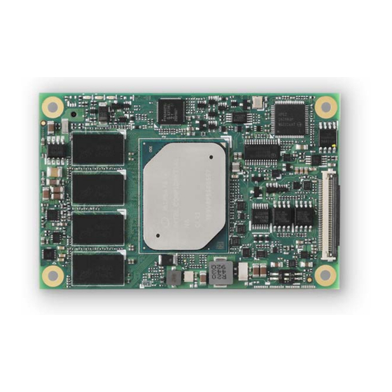
- Page 1 User’s Manual COM Express Mini Size Type 10 Module with Intel Atom®, Pentium®, Celeron® SoC Manual Rev.: Revision Date: July 16, 2020 Part Number: 50-1J088-1030 Leading EDGE COMPUTING...
- Page 2 Preface Copyright Copyright © 2018-2020 ADLINK Technology, Inc. This document contains proprietary information protected by copyright. All rights are reserved. No part of this manual may be reproduced by any mechanical, electronic, or other means in any form without prior written permission of the manufacturer.
-
Page 3: Table Of Contents
Table of Contents Preface ..........................ii List of Figures ........................vii List of Tables........................viii Introduction........................1 Specifications ......................3 2.1. Core System .......................3 2.2. Expansion Busses ......................3 2.3. Video........................... 4 2.4. Audio........................... 4 2.5. LAN..........................4 2.6. Multi I/O and Storage....................4 2.7. Serial I/O on Module ....................5 2.8. -
Page 4: Preface
3.3.9. USB 1.1/2.0........................18 3.3.10. USB 3.0 Extension......................19 3.3.11. USB Root Segmentation....................20 3.3.12. SPI (BIOS only) ........................ 21 3.3.13. Miscellaneous ........................21 3.3.14. SMBus..........................22 3.3.15. I2C Bus ..........................22 3.3.16. General Purpose I/O (GPIO).................... 22 3.3.17. Serial Interface Signals ....................23 3.3.18. - Page 5 7.2.5. Main >Access Level ......................45 7.3. Advanced........................46 7.3.1. Advanced > CPU Configuration..................46 7.3.2. Advanced > Graphics Configuration .................. 48 7.3.3. Advanced > Power Management..................49 7.3.4. Advanced > System Management..................50 7.3.5. Advanced > Thermal Management..................50 7.3.6.
- Page 6 Mechanical Information...................83 9.1. Board-to-Board Connectors..................83 9.2. Thermal Solution.......................84 9.2.1. Heat Spreaders........................84 9.2.2. Heat Sinks.......................... 84 9.2.3. Installation .......................... 84 9.3. Mounting Methods ....................86 9.4. Standoff Types......................87 Safety Instructions......................88 Getting Service.........................89 Preface...
-
Page 7: List Of Figures
List of Figures Figure 1: nanoX-AL Functional Block Diagram ..................8 Figure 2: nanoX-AL Mechanical Drawing....................9 Figure 3: nanoX-AL Connector, Switch and LED Locations ..............25 Figure 4: nanoX-AL and the DB40 Debug Module................25 Figure 5: cExpress Switch Locations ....................30 Figure 6: COM Express Mounting Methods .................. - Page 8 List of Tables Table 1: nanoX-AL Type 10 COM.0 Rev. 3.0 Pin Definitions ............... 11 Table 2: 40-pin Debug Connector Pin Definition ................... 27 Table 3: nanoX-AL LED Descriptions....................28 Table 4: MIPI60 Debug Header Pin Definition ..................29 Table 5: BIOS Select and Mode Configuration Switch Settings............30 Table 6: SEMA Onboard Voltage Monitor .....................
-
Page 9: Introduction
(8GB/16GB/32GB) and SD signals are available as build options. The nanoX-AL features a single onboard Gigabit Ethernet port, multiple PCIe lanes, USB 3.0 ports and USB 2.0 ports, and SATA 6 Gb/s ports. Support is provided for SMBus and I C. - Page 10 This page intentionally left blank. Introduction...
-
Page 11: Specifications
2. Specifications 2.1. Core System Dual or quad-core Intel Atom® processor E3900 SoC • Intel Atom® E3950 1.6/2.0GHz (Burst), 400-650MHz (Graphics) 12W (4C/1866) • Intel Atom® E3940 1.6/1.8GHz (Burst), 400-600MHz (Graphics) 9W (4C/1866) • Intel Atom® E3930 1.3/1.8GHz (Burst), 400-550MHz (Graphics) 6W (2C/1866) •... -
Page 12: Video
2.3. Video Intel® Generation 9 Low Power Graphics core architecture with up to 18 execution units Integrated on SoC supporting two independent displays • GPU Feature Support 3D graphics hardware acceleration • Support for DirectX12/11.3/10/9.3, OCL 2.0, OGL ES 3.0, OGL 4.3 •... -
Page 13: Serial I/O On Module
Boot Device Support Windows 10 Linux Enterprise (Yocto) Storage only eMMC 5.0 OS Installation eMMC 5.0 Note: eMMC and SD functionality as an OS installation device may change dependent on Intel updates. Please contact your local sales representative for more information. -
Page 14: Debug
2.10. Debug 40-pin flat cable connector to be used with DB-40 debug module Supports: BIOS POST code LED, BMC access, SPI BIOS flashing, power testpoints, debug LEDs MIPI60 60-pin header for debug of SoC (build option) 2.11. Power Specifications AT and ATX mode (AT mode startup controlled by SEMA Board Controller) Power Modes ATX: 12V ±5% / 5Vsb ±5% or AT = 12V ±5% Standard Voltage Input... -
Page 15: Operating Systems
2.16. Operating Systems • Standard Support Windows 10 (64-bit) • Linux (64-bit) • VxWorks (64-bit) • Extended Support (BSP) Linux (64-bit) • VxWorks (64-bit) Specifications... -
Page 16: Functional Diagram
2 UART (Tx/Rx) HSUART Super I/O TPM 2.0 LPC to UART (build option) LPC Bus SMBus GPIO SPI0 PCA9535 BIOS SPI1 4x GP0, 4x GPI (SDIO) BIOS GP I SEMA DDC I LM73 SPI_CS# Figure 1: nanoX-AL Functional Block Diagram Specifications... -
Page 17: Mechanical Drawing
2.18. Mechanical Drawing Top View Side View All are dimensions shown in millimeters. Tolerances should be ± 0.25mm, unless otherwise noted. The tolerances of the module connector locating peg holes (dimensions [9.8, 49]) should be ±0.10mm. Figure 2: nanoX-AL Mechanical Drawing Specifications... - Page 18 This page intentionally left blank. Specifications...
-
Page 19: Pinouts And Signal Descriptions
AB/CD Pin Definitions The nanoX-AL is a Type 10 module supporting USB 3.0 and DDI channel on the AB connector. All standard pins of the COM Express specification are described in the table below, including those not supported on the nanoX-AL. - Page 20 Row A Row B Name Name USB6- USB7- USB6+ USB7+ USB_6_7_OC# USB_4_5_OC# USB4- USB5- USB4+ USB5+ GND(FIXED) GND(FIXED) USB2- USB3- USB2+ USB3+ USB_2_3_OC# USB_0_1_OC# USB0- USB1- USB0+ USB1+ VCC_RTC ESPI_EN RSVD USB0_HOST_PRSNT GBE0_SDP SYS_RESET# LPC_SERIRQ / ESPI_CS1# CB_RESET# GND(FIXED) GND(FIXED) RSVD RSVD RSVD...
- Page 21 Row A Row B Name Name LVDS_A_CK+ / eDP_TX3+ DDI0_PAIR3+ LVDS_A_CK- / eDP_TX3- DDI0_PAIR3- LVDS_BKLT_CTRL / LVDS_I2C_CK / eDP_AUX+ eDP_BKLT_CTRL LVDS_I2C_DAT / eDP_AUX- VCC_5V_SBY GPI3 VCC_5V_SBY RSVD VCC_5V_SBY eDP_HPD VCC_5V_SBY PCIE_CLK_REF+ BIOS_DIS1# PCIE_CLK_REF- DDI0_HPD GND(FIXED) GND(FIXED) SPI_POWER DDI0_PAIR5+ SPI_MISO...
-
Page 22: Signal Description Terminology
3.2. Signal Description Terminology The following terms are used in the COM Express AB/CD Signal Descriptions below. Input to the Module Output from the Module Bi-directional input/output signal Open drain output I 3.3V Input 3.3V tolerant I 5V Input 5V tolerant O 3.3V Output 3.3V signal level O 5V... -
Page 23: Ab Signal Descriptions
3.3. AB Signal Descriptions 3.3.1. Audio Signals Signal Description PU/PD Comment HDA_RST# Reset output to CODEC, active low. PU 10k 3.3VSB 3.3VSB HDA_SYNC Sample-synchronization signal to the O 3.3V CODEC(s). HDA_BITCLK Serial data clock generated by the I/O 3.3V external CODEC(s). -
Page 24: Ddi0 Channel
3.3.3. DDI0 Channel Signal Description PU/PD Comment DDI0_PAIR0+ Digital Display Interface differential pairs O PCIE Pair 4 to Pair 6 DDI0_PAIR0- are not supported DDI0_PAIR1+ DDI0_PAIR1- DDI0_PAIR2+ DDI0_PAIR2- DDI0_PAIR3+ DDI0_PAIR3- DDI0_PAIR4+ DDI0_PAIR4- DDI0_PAIR5+ DDI0_PAIR5- DDI0_PAIR6+ DDI0_PAIR6- DDI0_HPD Digital Display Interface Hot-Plug Detect I 3.3V 100k DDI0_CTRLCLK_A... -
Page 25: Sata
Gigabit Ethernet Description PU/PD Comment low. 3.3VSB Gigabit Ethernet Controller 0 1000Mbit/sec link indicator, GBE0_LINK1000# A5 active low. 3.3VSB GBE0_CTREF Reference voltage for Carrier Board Ethernet channel 1 and 2 magnetics center tap. The reference voltage is determined by... -
Page 26: Express Card (Not Supported)
3.3.7. Express Card (Not supported) Signal Description PU/PD Comment EXCD0_CPPE# PCI ExpressCard: PCI Express I 3.3V PU 10k Not supported EXCD1_CPPE# capable card request 3.3V EXCD0_PERST# PCI ExpressCard: reset O 3.3V Not supported EXCD1_PERST# 3.3.8. LPC Bus Signal Description PU/PD Comment LPC multiplexed address, command LPC_AD[0:3]... -
Page 27: Usb 3.0 Extension
Signal Description PU/PD Comment module. An open drain driver from a USB current monitor on the carrier board may drive this line low. USB_2_3_OC# USB over-current sense, USB ports 2 and 3. A I 3.3VSB PU 10k Do not pull high pull-up for this line shall be present on the 3.3VSB... -
Page 28: Usb Root Segmentation
3.3.11. USB Root Segmentation xHCI Engine USB 2.0 USB 2.0 USB 2.0 USB 2.0 USB 3.0 Upgrade Port 1 USB 2.0 USB 2.0 USB 3.0 Upgrade Port 0 USB 3.0 USB 3.0 USB 2.0 USB 2.0 USB 2.0 Port 7 USB 2.0 Port 7 (Host/Device) USB 3.0... -
Page 29: Spi (Bios Only)
3.3.12. SPI (BIOS only) Signal Description PU/PD Comment SPI_CS# Chip select for Carrier Board SPI BIOS Flash. O 3.3VSB PU 10k 3.3VSB SPI_MISO Data in to module from carrier board SPI BIOS flash. I 3.3VSB SPI_MOSI Data out from module to carrier board SPI BIOS flash. -
Page 30: Smbus
3.3.14. SMBus Signal Description PU/PD Comment SMB_CK System Management Bus bidirectional clock line. Power I/O OD PU 8k2 sourced through 5V standby rail and main power rails. 3.3VSB 3.3VSB SMB_DAT# System Management Bus bidirectional data line. Power I/O OD PU 8k2 sourced through 5V standby rail and main power rails. -
Page 31: Serial Interface Signals
3.3.17. Serial Interface Signals Signal Description PU/PD Comment SER0_TX General purpose serial port transmitter (TTL PU 4k7 Power rail tolerance 5V/12V level output) CMOS There shall be PD on carrier board General purpose serial port receiver (TTL level PU 4k7... -
Page 32: Power And Ground
Signal Description PU/PD Comment BATLOW# Battery low input. This signal may be driven low by I 3.3VSB PU 10k external circuitry to signal that the system battery is 3.3VSB low, or may be used to signal some other external power-management event. LID# A103 LID button. -
Page 33: Module Interfaces
PICMG standard specification 4.1. Connector, Switch and LED Locations Figure 3: nanoX-AL Connector, Switch and LED Locations Note: The optional MIPI60 Debug Header is located on the breakout PCB. nanoX-AL and the DB40 Debug Module (the diagram below is for illustration purpose only) -
Page 34: 40-Pin Debug Connector
4.2. 40-pin Debug Connector FPC Connector Type: FCI 59GF Flex 10042867 Pin Orientation 40-pin Debug Connector Pin Definition on the COM Express Module Pin # Interface Siganls Remark RSVD SMC_STATUS Connect to LED BIOS_MODE Connect to Jumper for Debug For SMC Debug SEL_BIOS Connect to Jumper for Debug POSTWDT_DIS#... -
Page 35: Table 2: 40-Pin Debug Connector Pin Definition
Pin # Interface Siganls Remark LPC_AD0 LPC_AD1 LPC_AD2 LPC_AD3 LPC_FRAME# LPC Debug card Interface CLK33_LPC RST# BIOS_DIS0 GND2 3V3_LPC System power 3.3V provided from COM module SPI_BIOS_CLK SPI_BIOS_MOSI SPI_BIOS_MISO SPI_BIOS_CS1# SPI Program Interface SPI_BIOS_CS0# GND1 SPI Power Input from flash tool to module. -
Page 36: Status Leds
Rebooted after PWRBTN WD LED = LED OFF Rebooted after RESET BTN WD LED = LED OFF Note: only a RESET not initiated by the BMC can clear the WD LED (user action) Table 3: nanoX-AL LED Descriptions Module Interfaces... -
Page 37: Mipi60 Debug Header (Build Option)
4.4. MIPI60 Debug Header (build option) Not all pins of the Intel MIPI60 connector are connected to the CombiProbe Intel x86/x64 MIPI60-C. ® Signal XDP Signal VREF_DEBUG TCK0 Open Drain Reset Out Reset In No Connect TRST_N PREQ_N PRDY_N... -
Page 38: Switch Settings
4.5. Switch Settings Switch Locations BIOS Select and Mode Configuration Switch Figure 5: cExpress Switch Locations BIOS Select and Mode Configuration Switch Module has two BIOS chips and BIOS operation can be configured to "PICMG" and "Failsafe" modes using BSW1, Pin 2. -
Page 39: Smart Embedded Management Agent (Sema)
5. Smart Embedded Management Agent (SEMA) The onboard microcontroller (BMC) implements power sequencing and Smart Embedded Management Agent (SEMA) functionality. The microcontroller communicates via the System Management Bus with the CPU/chipset. The following functions are implemented: ‧ Total operating hours counter. Counts the number of hours the module has been run in minutes. -
Page 40: Board Specific Sema Functions
5.1.2. Main Current The BMC of the nanoX-AL implements a current monitor. The current can be read by calling the SEMA function “Get Main Current”. The function returns four 16-bit values divided in high-byte (MSB) and low-byte (LSB). These 4 values represent the last 4 currents drawn by the board. -
Page 41: Exception Codes
5.1.4. Exception Codes In case of an error, the BMC drives a blinking code on the blue Status LED (LED1). The same error code is also reported by the BMC Flags register. The Exception Code is not stored in the Flash Storage and is cleared when the power is removed. - Page 42 This page intentionally left blank. Smart Embedded Management Agent (SEMA)
-
Page 43: System Resources
6. System Resources 6.1. System Memory Map Address Range (hex) Description FF00_0000 – IFAW (BIOS) FFFF_FFFF FED0_0000 – HPET FEDF_33FF FEC0_0000 – IOAPIC FECF_FFFF 0K –1MB DOS DRAM 6.2. I/O Map I/O Address IOSF Primary Target IOSF SB Target 000h–01Fh... - Page 44 I/O Address IOSF Primary Target IOSF SB Target 066h P2SB LPC/eSPI 067h P2SB ITSS (CPU I/F) 070h P2SB ITSS (CPU I/F), RTC, PMC 071h P2SB RTC, PMC 072h–073h P2SB RTC, PMC 073h P2SB RTC, PMC 074h P2SB RTC, PMC 075h P2SB RTC, PMC 076h–077h...
-
Page 45: Interrupt Request (Irq) Lines
I/O Address IOSF Primary Target IOSF SB Target 170h–177h P2SB Terminate 2F8h–2FFh P2SB Serial Port 240h–24Fh P2SB Serial Port 2F8h–2FFh P2SB Serial Port 376h P2SB Terminate 3F6h P2SB Terminate 3F8h–3FFh P2SB Serial Port 4D0h–4D1h P2SB ITSS (interrupt) CF9h P2SB ITSS (CPU I/F) 6.3. - Page 46 IO APIC Pin Routing Option for configurable sources including internal ACPI/PCI devices Option for configurable sources including internal PIRQA, internal ACPI/PCI devices PIRQB (xHCI) Option for configurable sources including internal PIRQC, internal ACPI/PCI devices Option for configurable sources including internal PIRQD, internal ACPI/PCI devices Option for configurable sources including internal PIRQE, SCI, TCO, internal ACPI/PCI devices and HPET...
- Page 47 IO APIC Pin Routing reserved reserved reserved reserved 50 - 119 GPIO (Not for end user) Note: These IRQs can be used for PCI devices when onboard device is disabled. APIC Mode IRQ# Typical Intterupt Resource Connected to Pin...
-
Page 48: Pci Configuration Space Map
6.4. PCI Configuration Space Map Logical Function Device Function Host Bridge DPTF (Camarillo) NPK (PSF ghost) Iunit Reserved (CSE) P2SB Shared SRAM Audio CSE-HECI1 CSE-HECI2 CSE-HECI3 CSE-fTPM (PSF ghost) CSE-HOFFL SATA PCIe-A 1 PCIe-A 2 PCIe-A 3 PCIe-B 1 (multpixted with USB3.0 port) PCIe-B 2 (connect to onboard LAN) PCIe-A 1... -
Page 49: Pci Interrupt Routing Map
Logical Function Device Function I2C 5 I2C 6 I2C 7 UART 0 UART 1 UART 2 UART 3 SPI 0 SPI 1 SPI 2 SD Card eMMC SDIO SMBUS 6.5. PCI Interrupt Routing Map PCIE PCIE PCIE PCIE Mobile... -
Page 50: Smbus Address Table
I2C0 I2C1 I2C2 I2C3 I2C4 I2C5 I2C6 I2C7 Line Int0 INTA:27 INTF:31 Int1 INTB:28 INTB:32 Int2 INTC:29 INTC:33 Int3 INTD:30 INTD:34 SPI1 SPI3 SPI3 SD Host #0 SD Host #1 SD Host #2 SD Host #3 Line Int0 INTA:35 INTC:15 INTD:39 INTH:38 INTB:37... -
Page 51: Bios Setup
7. BIOS Setup 7.1. Menu Structure This section presents the six primary menus of the BIOS Setup Utility. Use the following table as a quick reference for the contents of the BIOS Setup Utility. The subsections in this section describe the submenus and setting options for each menu item. -
Page 52: Main
7.2. Main The Main Menu provides read-only information about your system and also allows you to set the System Date and Time. Refer to the tables below the screen shot of this menu for details of the submenus and settings. 7.2.1. -
Page 53: Main > Board Information
7.2.3. Main > Board Information Feature Options Description Board Information Submenu Board Information Info only Serial Number Info only Display SEMA serial Number. Manufacturing Date Info only Display SEMA manufacturing date. Last Repair Date Info only Display SEMA last repair date. -
Page 54: Advanced
7.3. Advanced This menu contains the settings for most of the user interfaces in the system. 7.3.1. Advanced > CPU Configuration Feature Options Description CPU Configuration Info only Socket 0 CPU Information Submenu Socket Specific CPU Information. Stocket 0 CPU information Info only CPU Signature Info only... - Page 55 Feature Options Description C-State Auto Demotion Disabled Configure C-State Auto Demotion Disabled C-State Un-demotion Configure C-State Auto Un-demotion Power Limit 1 Enable Disabled Enable / Disable Power Limit 1 Enabled Power Limit 1 Info Only Display Power Limit 1 Power Watts.
-
Page 56: Advanced > Graphics Configuration
Feature Options Description VT-d Disabled Enable / Disable CPU VT-d Enabled Disabled When a processor thermal sensor trips (either core), Bi-directional PROCHOT the PROCHOT# will be driven. Enabled If bi-direction is enabled, external agents can drive PROCHOT# to throttle the processor. When Enabled, the processor will limit the maximum Limit CPUID Maximum Disabled... -
Page 57: Advanced > Power Management
7.3.3. Advanced > Power Management Feature Options Description Power Management Info only Enable ACPI Auto Configuration Enables or Disables BIOS ACPI Auto Configuration. Disabled Enabled Enable Hibernation Disabled Enable or Disable System ability to Hibernate (OS/S4 Sleep State). Enabled This option maybe not effective with some OS. -
Page 58: Advanced > System Management
7.3.4. Advanced > System Management Feature Options Description System Management Info Only Version Info Only Display SEMA Module Version. SEMA Firmware Info Only Display SEMA Firmware Version. Build Date Info Only Display SEMA Firmware Build Date. SEMA Bootloader Info Only Display SEMA Bootloader Version. -
Page 59: Advanced > Watchdog Timer
7.3.5.1. Advanced > Thermal Management > Thermal and Fan Speed Feature Options Description Temperatures and Fan Speed Info Only CPU Temperature Info Only Current Info Only Display Current CPU Temperature Board Temperature Info Only Current Info Only Display Current Board Temperature... - Page 60 Feature Options Description W83627DHG Info Only Serial Port 1 Configuration Submenu Set Parameters of Serial Port 1 (COMA). Serial Port 2 Configuration Submenu Set Parameters of Serial Port 2 (COMB). 7.3.8.1. Advanced > Super IO Configuration > Serial Port 1 Configuration (NCT5104D) Feature Options Description...
-
Page 61: Advanced > Serial Console Redirection
7.3.8.4. Advanced > Super IO Configuration > Serial Port 2 Configuration (W83627DHG) Feature Options Description Serial Port 2 Configuration Submenu Set Parameters of Serial Port 2 (COMB). Serial Port 2 Configuration Info only Serial Port Disableed Enable or Disable Serial Port (COM). - Page 62 Feature Options Description Console Redirection Enabled Console Redirection Enable or Disable. Disabled The settings specify how the host computer and the Console Redirection Settings Submenu remote computer (which the user is using) will exchange data. Both computers should have the same or compatible settings.
-
Page 63: Advanced > Usb
Feature Options Description VT-UTF8 Combo Key Support Enable VT-UTF8 Combination Key Support for Enabled Disabled ANSI/VT100 terminals Enabled On Legacy OS, the Number of Rows and Columns Resolution 100x31 supported redirection Disabled Legacy OS Redirection On Legacy OS, the Number of Rows and Columns... -
Page 64: Advanced > Network
Feature Options Description Device reset time-out 10 sec USB mass storage device Start Unit command time- out. 20 sec 30 sec 40 sec Device power-up delay Maximum time the device will take before it properly Auto Manual reports itself to the Hot Controller. ‘Auto’... -
Page 65: Advanced > Trusted Computing
Feature Options Description TPM2.0 UEFI Spec Version TCG_1_2 Select the TCG2 Spec Version Support, TCG_1_2: the Compatible mode for Win8/Win10, TCG_2 TCG_2: Support new TCG2 protocol and event format for Win10 or later Physical Presence Spec Version Select to Tell O.S. to support PPI Spec Version 1.2 or 1.3. -
Page 66: Chipset
7.4. Chipset 7.4.1. Chipset > North Bridge Feature Options Description Memory Information Info only Total Memory Info only Display Total Memory Size. Memory Vlotage Info only Display Memory Vlotage. Memory Slot0 Info only Display Installed Memory Slot0 Information. Memory Slot1 Info only Display Installed Memory Slot1 Information. - Page 67 Feature Options Description DDI port 1 No Device DDI port 1 function choose to Display Port or HDMI. Display Port HDMI DisplayPort with HDMI/DVI Compatible LFP Panel Type Select LFP panel used by Internal Graphics Device by Auto 640x480 selecting the appropriate setup item.
-
Page 68: Chipset > South Cluster Configuration
Feature Options Description DVMT Total Gfx Mem 128M Select DVMT5.0 Total Graphic Memory size used by the Internal Graphics Device 256M 7.4.4. Chipset > South Cluster Configuration Feature Options Description HD-Audio Configuration Submenu HD-Audio Configuration Setting. PCI Express Configuration Submenu PCI Express Configuration Setting. - Page 69 Feature Options Description PCI ExpressRoot Port 3 Submenu Control the PCI Express Root Port. AUTO: To disable unused root port automatically for the most optimum power savings. Enable: Enable PCIe root port Disable: Disable PCIe root port Chipset > South Cluster Configuration > PCI Express Configuration > PCI Express Root Port 1...
- Page 70 Feature Options Description Extra Bus Reserved Extra Bus Reserved (0-7) for bridges behind this Root Bridge Reserved Memory and Prefetchable Memory (1- Reserved Memory 20MB) Range for this Root Bridge Reserved I/O Reserved I/O (4K/8K/12K/16K/20K) Range for this Root Bridge PCH PCIe LTR Info only Configuration...
- Page 71 Feature Options Description PCI Express Completion Timer TO Enable/Disable. Default Setting 16-15 ms 65-210 ms 260-900 ms 1-3.5 s Disable SEFE Root PCI Express System Error on Fatal Error Disable Enable Enable/Disable SENFE Root PCI Express System Error on Non-Fatal Error...
- Page 72 Chipset > South Cluster Configuration > PCI Express Configuration > PCI Express Root Port 3 Feature Options Description PCI Express Root Port 3 Disable Control the PCI Express Root Port. Enable AUTO: To disable unused root port automatically for Auto the most optimum power savings.
- Page 73 Feature Options Description PCH PCIe LTR Info only Configuration Disable PCH PCIE LTR PCH PCIE Latency Reporting Enable/Disable Enable Snoop Latency Override Disabled Snoop Latency Override for PCH PCIE. Manual Disabled: Disable override. Auto Manual: Manually enter override values.
- Page 74 Feature Options Description Spin Up Device If enabled for any of ports Staggerred Spin Up will be Disabled Enabled performed and only the drives which have this option enabled will spin up at boot. Otherwise all drives spin up at boot. SATA Device Type Identify the SATA port is connected to Solid State Hard Disk Drive...
- Page 75 7.4.4.4. Chipset > South Cluster Configuration > SSC Configuration Feature Options Description SSC SD Card Support (D27:F0) Disabled Enable / Disable SCC SD Card Support. Enabled SCC eMMC Support (D28:F0) Disabled Enable / Disable SCC eMMC Support. Enabled eMMC Max Speed Select the eMMC max Speed allowed.
- Page 76 7.4.4.6. Chipset > South Cluster Configuration > Miscellaneous Configuration Feature Options Description Miscellaneous Configuration Info only State After G3 Specify what state to go to when power is re-applied S0 State S5 State after a power failure (G3 state). Last State S0 State: System will boot directly as soon as power applied.
-
Page 77: Security
7.5. Security 7.5.1. Security > Password Description Feature Options Description Password Description Info only Setup Administrator Password Enter Password Set Setup Administrator Password User Password Enter Password Set User Password Secure Boot Submenu Customizable Secure Boot settings. System Mode... -
Page 78: Boot
7.6. Boot 7.6.1. Boot > Boot Configuration Feature Options Description Boot Configuration Info only Setup Prompt Timeout Number of seconds to wait for setup activation key. 65535(0xFFFF) means indefinite waiting. Bootup NumLock State Select the keyboard Number state. Ouiet Boot Disabled Select the keyboard NumLock state. -
Page 79: Save & Exit
7.7. Save & Exit Feature Options Description Save Changes and Exit Exit system setup after saving the changes. Discard Changes and Exit Exit system setup without saving any changes. Save Change and Reset Reset the system after saving the changes. - Page 80 This page intentionally left blank. BIOS Setup...
-
Page 81: Bios Checkpoints, Beep Codes
8. BIOS Checkpoints, Beep Codes This section of this document lists checkpoints and beep codes generated by AMI Aptio BIOS. The checkpoints defined in this document are inherent to the AMIBIOS generic core, and do not include any chipset or board specific checkpoint definitions. -
Page 82: Status Code Ranges
8.1. Status Code Ranges Status Code Description Range 0x01 – 0x0B SEC execution 0x0C – 0x0F SEC errors 0x10 – 0x2F PEI execution up to and including memory detection 0x30 – 0x4F PEI execution after memory detection 0x50 – 0x5F PEI errors 0x60 –... -
Page 83: Sec Beep Codes
SEC Error Codes 0x0C – 0x0D Reserved for future AMI SEC error codes 0x0E Microcode not found 0x0F Microcode not loaded 8.2.2. SEC Beep Codes None 8.2.3. PEI Phase Status Code Description Progress Codes 0x10 PEI Core is started... - Page 84 Status Code Description 0x35 CPU post-memory initialization. Boot Strap Processor (BSP) selection 0x36 CPU post-memory initialization. System Management Mode (SMM) initialization 0x37 Post-Memory North Bridge initialization is started 0x38 Post-Memory North Bridge initialization (North Bridge module specific) 0x39 Post-Memory North Bridge initialization (North Bridge module specific) 0x3A Post-Memory North Bridge initialization (North Bridge module specific) 0x3B...
-
Page 85: Pei Beep Codes
Status Code Description S3 Resume Error Codes 0xE8 S3 Resume Failed 0xE9 S3 Resume PPI not Found 0xEA S3 Resume Boot Script Error 0xEB S3 OS Wake Error 0xEC-0xEF Reserved for future AMI error codes Recovery Progress Codes 0xF0... -
Page 86: Dxe Status Codes
8.2.5. DXE Status Codes Status Code Description 0x60 DXE Core is started 0x61 NVRAM initialization 0x62 Installation of the South Bridge Runtime Services 0x63 CPU DXE initialization is started 0x64 CPU DXE initialization (CPU module specific) 0x65 CPU DXE initialization (CPU module specific) 0x66 CPU DXE initialization (CPU module specific) 0x67... - Page 87 Status Code Description 0x95 PCI Bus Request Resources 0x96 PCI Bus Assign Resources 0x97 Console Output devices connect 0x98 Console input devices connect 0x99 Super IO Initialization 0x9A USB initialization is started 0x9B USB Reset 0x9C USB Detect 0x9D USB Enable 0x9E –...
-
Page 88: Dxe Beep Codes
Status Code Description 0xB8 – 0xBF Reserved for future AMI codes 0xC0 – 0xCF OEM BDS initialization codes DXE Error Codes 0xD0 CPU initialization error 0xD1 North Bridge initialization error 0xD2 South Bridge initialization error 0xD3 Some of the Architectural Protocols are not available 0xD4 PCI resource allocation error. -
Page 89: Oem-Reserved Checkpoint Ranges
Status Code Description 0x10 System is waking up from the S1 sleep state 0x20 System is waking up from the S2 sleep state 0x30 System is waking up from the S3 sleep state 0x40 System is waking up from the S4 sleep state 0xAC System has transitioned into ACPI mode. - Page 90 This page intentionally left blank. BIOS Checkpoints, Beep Codes...
-
Page 91: Mechanical Information
9. Mechanical Information 9.1. Board-to-Board Connectors To allow for different stacking heights, the receptacles for COM Express carrier boards are available in two heights: 5 mm and 8 mm. When 5 mm receptacles are chosen, the carrier board should be free of components. -
Page 92: Thermal Solution
9.2. Thermal Solution 9.2.1. Heat Spreaders The function of the heat spreader is to ensure an identical mechanical profile for all COM Express modules. By using a heat spreader, the thermal solution that is built on top of the module is compatible with all COM Express modules. - Page 93 Step 3: Put heatsink on the COM Express module and assemble the heatsink onto the COM Express module. Use the four M2.5, L=6mm screws provided to fasten the heatsink to the module. Mechanical Information...
-
Page 94: Mounting Methods
9.3. Mounting Methods There are several standard ways to mount the COM Express module with a thermal solution onto a carrier board. In addition to the choice of 5 mm or 8mm board-to-board connectors, there is the choice of Top and Bottom mounting. -
Page 95: Standoff Types
9.4. Standoff Types The standoffs available for Top and Bottom mounting methods are shown below. Note that threaded standoffs are DIP type and through-hole standoffs are SMT type. Other types not listed are available upon request. 5mm through-hole standoff (SMT type) -
Page 96: Safety Instructions
Safety Instructions Read and follow all instructions marked on the product and in the documentation before you operate your system. Retain all safety and operating instructions for future use. • Please read these safety instructions carefully. • Please keep this User‘s Manual for later reference. •... -
Page 97: Getting Service
5215 Hellyer Avenue, #110, San Jose, CA 95138, USA Tel: +1-408-360-0200 Toll Free: +1-800-966-5200 (USA only) Fax: +1-408-360-0222 Email: info@adlinktech.com ADLINK Technology (China) Co., Ltd. Address: 300 Fang Chun Rd., Zhangjiang Hi-Tech Park, Pudong New Area Shanghai, 201203 China Tel: +86-21-5132-8988 Fax: +86-21-5132-3588 Email: market@adlinktech.com...
Need help?
Do you have a question about the nanoX-AL and is the answer not in the manual?
Questions and answers