Table of Contents
Advertisement
Quick Links
Advertisement
Table of Contents

Related Manuals for ICS ELECTRONICS 4863


Summary of Contents for ICS ELECTRONICS 4863
- Page 1 ELECTRONICS MODEL 4863 GPIB Parallel Interface MODEL 2363 Serial Parallel Interface...
- Page 2 MODEL 4863 GPIB Parallel Interface Model 2363 Serial Parallel Interface Instruction Manual ELECTRONICS division of Systems West Inc. 7034 Commerce Circle, Pleasanton, CA 94588 Phone 925.416.1000, Fax 925.416.0105 Publication Number 120143 Web Site http://www.icselect.com October 2006 Edition Rev 9...
- Page 3 The Model 4863 and 2363 have been tested and found to comply with the limits for a Class A computing device pursuant to Subpart J of...
- Page 4 Commands, SCPI Commands, Single Letter Commands, Programming Guidelines and Serial Interface Operation. Theory of Operation Describes the 4863 and 2363's Theory of Operation and provides Block Diagram Descriptions. Troubleshooting and Repair Theory of Operation, Self test error codes, Troubleshooting guide, and Repair Information.
- Page 5 This page left intentionally blank...
- Page 6 48 mA. The interfaces can also monitor 15 of the digital lines and report any changes to the Bus Controller. The 4863 transfers data either as the parameter in a command or as a transparent data string. Data can be formatted as decimal or hex characters or unformatted binary bytes.
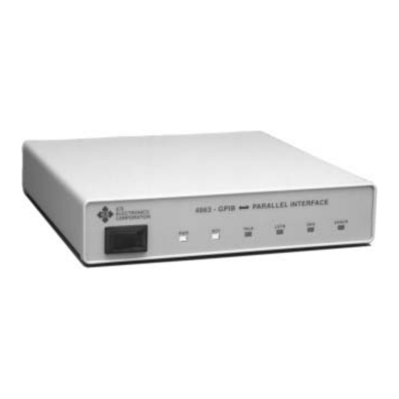
- Page 7 LEDs before displaying their normal Power-on - Ready condition. The 4863 is a member of ICS's Minibox product family and is packaged in a small metal case that is less than 1U (1.6 inches) in height. The front panel contains the power switch and LEDs which indicate the unit's status.
- Page 8 MODEL 4863/2363 SPECIFICATIONS 1.3.1 4863/2363 Model Numbers and Options The following specifications apply to all 4863 and 23633 models. Options for your unit may be found by comparing the list below to those listed on the serial label on your unit.
- Page 9 1.3.2 OEM Board Part Numbers and Configurations OEM Board versions of the 4863 and 2363 are available in the configurations shown in Table 1-1. On OEM Boards, the GPIB connector is a vertical header that mates with one of ICS's GPIB Connector/Address Switch Assemblies which may be used to mount an Address Switch and a GPIB Connector on the user's rear panel.
- Page 10 GPIB Addressing The 4863 has three, user selectable address modes. In the Single address mode, the 4863 responds to a single primary address for all commands. In the Dual mode, the 4863 responds to two consecutive primary addresses. The lower address is used for commands and setting the device's address, the upper address is used for transparent data transfer.
- Page 11 1.4.5 SCPI Parser The 4863 and 2363 include an extended SCPI parser that complies with the SCPI Standard Version 1994.0. 1.4.6 Buffers The 4863 and 2363 use the same input and output buffers. Buffer size is 1024 bytes.
- Page 12 SERIAL INTERFACES (2363) Model 2363s have their RS-232 and RS-485 signals on an RS-530 compatible 25-pin female connector on the rear panel. The 2363 automatically responds to the serial port that received the last message. 1.5.1 Baud Rate and Character Format Baud Rate Any rate from 300 to 115,200 baud.
- Page 13 1.5.4 Buffers Input Buffer 1024 bytes 1.5.5 RS-232 Transmission Protocol 1.5.5.1 Echos and Prompts The 2363 returns a prompt when ready for the next command. If Echo is enabled, the prompt character is lined along the left edge of the screen. The CNTL-E and CNTL-F commands turn echo on and off and change the prompt sequence and message terminators as follows: Command Echo...
- Page 14 1.5.6 RS-485 Basic Protocol When the Network mode is set to Off, the RS-485 interface operates as does the RS-232 interface with Echo OFF. All responses messages are terminated with a linefeed character (LF). A '> LF' prompt is sent after each command or after the response message.
- Page 15 An acknowledgment packet is: ACK Addr ESR_Register_Value ETX Checksum ACK Addr Query_response ETX Checksum An NAK packet is: NAK Addr ESR_Register_Value ETX Checksum Where: ASCII characters 0 to 1F hex are reserved for message control. ASCII characters 20-7F are for address and data. Address character is 30-3F hex.
- Page 16 DIGITAL SIGNAL SPECIFICATIONS The 4863/2363's Digital I/O signals have the following specifications: 1.6.1 Data Lines Number 48 with internal 33 Kohm pullups to + 5 Vdc Input High >=2.4 Vdc or open circuit Levels < 0.5 Vdc at 200 µA...
- Page 17 Monitored Digital Inputs The first fifteen Digital I/O lines (CH1-15) are sampled at an approximate 1 kHz rate and the values placed in the Questionable Register in the 4863/ 2363's IEEE-488.2 Status Reporting Structure. Changes may be used to generate a Service Request. The digital input lines are reported at the...
- Page 18 A false input inhibits data transfer. Status B may be used as a request for the 4863 to go to the local state. The 4863 will deassert the Remote output in response to a true Status B input if the unit is not in the GPIB Local Lockout State.
- Page 19 Data Lines EDR Input TdLoad Inhibit Output Talk Address GPIB DAV Pulses TdTDav TdLoad is time to load data after being addressed to talk Data must remain stable until Inhibit goes false TdTDav is the time to output first byte on GPIB Bus Figure 1-1 Input Data Timing DAV Pulses...
- Page 20 1.6.12 Timing Chart The times in Table 1-2 are for a 4863 with a 20 MHz clock. TABLE 1-2 4863 TIMING Symbol Command/Notes Time TdLoad Loading time for 6 hex characters 4.0 ms TdTDAV Delay to first Talk DAV Pulse 0.7 ms...
- Page 21 CONFIGURABLE FUNCTIONS Table 1-3 lists the 4863's configuration parameters and their factory settings. Table 1-4 lists the 2363's factory settings. The configuration parameters are saved in nonvolatile Flash memory. TABLE 1-3 4863 CONFIGURATION PARAMETERS Command Function Factory Setting :ADDRESS Sets 4863's GPIB bus address...
- Page 22 TABLE 1-4 2363 CONFIGURATION PARAMETERS Command Function Factory Setting :BAUD Sets 2363's baud rate 9600 :PARity Sets 2363's serial parity NONE :BITS Sets 2363's data bits : :SBITs Sets 2363's stop bits : :NETwork Sets RS-485 protocol OFF # :ADDRess Sets 2363's address for network use :INPut Sets number of Talk bytes...
- Page 23 GPIB or network address by blinking it address on the front panel LEDs for a half a second. If the 4863 is set for dual secondary addresses, the address is blinked twice. The LED...
- Page 24 - 7.0" L x 7.0" W x 1.26" H (17.78 cm L x 17.78 cm W x 3.20 cm H) (See Figure 1-6) Weight - 3 lbs (1.4 kg) including adapter (4863) Temperature - Operating-10° C to +55° C Storage -40°...
- Page 25 Figure 1-5 Outline Dimensions 1-20...
- Page 26 7.00 .150 62/42/21 .150 Serial Header Digital I/O Connector Remote 7.00 Header 43/22/1 GPIB Header MAX COMPONENT HEIGHT 1.08 4-40 UNC STAND-OFF .187 in .25 DIA X .187 Figure 1-6 4863 OEM Board Outline Dimensions 1-21...
- Page 27 20780 and complies with EEC Standards EN 55022 and 50082-1. CE Certificate of Compliances reproduced in Figures 1-7 and 1-8. UL/CSA/VDE AC Wall adapter has applicable UL/CSA/VDE and CE approval. GPIB TO DIGITAL INTERFACE 4863 1996 Figure 1-7 4863 Certificate of Compliance 1-22...
- Page 28 Figure 1-8 2363 Certificate of Compliance 1-23...
- Page 29 CM long. 90 CM standard) 113642-L Vertical GPIB Connector/Address Switch Assembly (L= cable length in CM, 90 CM standard) 125076 Kit - Mating Serial Header Connector 902270 Mating Digital I/O Connector for 4863 OEM Board 902105 Hood (Plastic) for 902270 Digital I/O Connector 1-24...
- Page 30 Model 4863 or Model 2363 Parallel Interface AC Power Adapter Mating Digital I/O Connector and hood 4863/2363 Instruction Manual Support CD-ROM 4863 and 2363 OEM boards include the mating Digital I/O connector, Instruction Manual and Support CD-ROM.
- Page 31 FACTORY CONFIGURATION When shipped, the 4863 and 2363 are set to the configurations listed in Tables 1-3 and 1-4. The configurable parameters are stored in Flash memory and can be queried and changed by the user. CONFIGURATION DIRECTIONS Configuring a 4863 or 2363 is a multistep process. First design the connections between the digital interface and the external device as directed in Section 2.8.
- Page 32 THE SUPPORT CD The Support CD-ROM contains Configuration Programs, useful utility programs and example programs for ICS's interface products. The Configuration Programs folder contains DOS and Windows configuration programs that walk the user through a menu to configure the card's power- on condition.
- Page 33 First copy the configuration program to a directory on your hard drive as directed in 2.5. Connect the 4863 to the GPIB controller card in the PC as shown in Figure 2-1. Plug the AC adapter plug into the DC jack in the 4863’s rear panel.
- Page 34 Return e.g. 4863 <return> for the Model 4803 2363 <return> for the Model 2303 Cycle Power The program may ask that you turn the unit's power off and on.
- Page 35 entered from the GPIBkybd program or as part of the user's program. After the last selection, the program will ask if the unit is configured correctly. Enter N to go back and change the configuration; Y to continue. Saving the New Settings The program will ask if you want to save the current configuration.
- Page 36 CONFIGURING FROM THE GPIBKYBD AND OTHER PROGRAMS The 4863 can be configured from any GPIB bus controller by using the following procedure and a interactive control program like ICS’s GPIBkybd program. The example commands can also be imported into any program language.
- Page 37 Use the equivalent OUTPUT and ENTER type statements in your computer's program to send the configuration commands to the 4863. Each new configuration statement should be followed with a query to verify that the unit accepted the new setting or visually monitor the ERR LED.
- Page 38 i.e., to change the unit's GPIB address to dual secondary OUTPUT 720; "SYST:COMM:GPIB:ADDR:MODE DUAL" OUTPUT 72000;"SYST:COMM:GPIB:ADDR:MODE?" ENTER 72000, A$ PRINT A$ 'displays the query response With the NI 488.2 command set, secondary addresses are offset by 96 and multiplied by 256 to be in the upper byte of the address variable.
- Page 39 REM 4863 COMMAND ENTRY / READOUT PROGRAM PRINT “” PRINT “” PRINT “4863 COMMAND ENTRY PROGRAM” DIM A$[100] DIM B$[200] Devadr=4 Adr=704 ON TIMEOUT 7,5 GOTO 820 ON INTR 7 GOSUB 620 Mask=2 ENABLE INTR 7;Mask GOSUB 470 CLEAR Adr WAIT .1...
- Page 40 REM Help Menu PRINT PRINT “HELP for this menu” PRINT “SPOL! to Serial Poll Device address” PRINT “DATA! select DATA address” PRINT “CMD! select CMD address” PRINT “ENTER to read data from Device address” PRINT A$=”XXX” RETURN REM Serial Poll PRINT PRINT “********** SRQ INTERRUPT OCCURRED! **********”...
- Page 41 100 REM BASIC GPIB ADDRESS SETTING PROGRAM 110 DIM A$[100], B$[20] 120 CLEAR 7 130 WAIT .1 140 INPUT “Enter Current Device Address (0-30):”, Devadr 150 Adr=Devadr+700 160 SEND 7; UNL LISTEN Devadr 170 WAIT .1 180 A$=”SYST:COMM:GPIB:ADDR?” 190 OUTPUT Adr; A$ END 200 ENTER Adr;...
- Page 42 The 4863 has two connectors on the rear panel. J1 is the IEEE 488/GPIB bus connector and J2 is the Digital I/O Connector. Any standard IEEE 488 bus cable may be used to connect the 4863 to the bus controller as shown in Figure 2-4. ICS can provide IEEE Bus Cables with standard double headed connectors or straight-in connectors.
- Page 43 2.7.2 2363 Connections The 2363 has two connectors on the rear panel. J1 is the serial interface connector and J2 is the Digital I/O Connector. 2.7.2.1 RS-232 Connections The 2363's serial interface connector (J1) is a DB-25S 25 pin female connector with both RS-232 and RS-485 signals.
- Page 44 2.7.2.2 RS-485 Connections The 2363 has two RS-485 signals on Pins 14 and 16 for a half-duplex RS- 485 connection. Pin 14 has the Tx/Rx+ signal; pin 16 has the Tx/Rx- signal. The 2363 contains an internal network termination circuit with 1 Kohm pullup and pulldown resistors and a 220 ohm termination resistor.
- Page 45 The Digital I/O connector on OEM Boards is the same as on the standard 4863/2363. Use the mating connector supplied with the unit and follow the directions in Sections 2.9 to connect the OEM Board to the host equipment.
- Page 46 The Serial Header J4 is a 10-pin male header with 0.025 square pins on 0.1 centers. Pin 8 is the key position and is omitted from the header. The Serial Header location on the 4863 lower board is shown in Figure 2-6. Signal pin assignments are listed in Table 2-2.
- Page 47 + 5 Vdc thru 3 KΩ 2.7.3.3 LED Header The LED Header J7 contains the signals for driving a duplicate set of 4863 LEDs. The LED Header is a 7-pin male header with 0.025 square pins on 0.1 centers. The header is not keyed. The LED header location on the 4863 OEM board is shown in Figure 2-6.
- Page 48 TABLE 2-4 LED HEADER PIN ASSIGNMENTS Signal Function + 5 Vdc Signal Ground ERR# ERROR LED SRQ# SRQ LED LSTN# LSTN LED TALK# TALK LED RDY# READY LED The LED drive signals are low true and designed to sink 15 mA of extra current to operate the remote LEDs.
- Page 49 DIO8 GRN 3 GROUND BLU 3 (a) J2 GPIB/Sw Connector Layout Notes: Switch shown set to address 4 (See Figure 1-6 (b) GPIB Address Switch for connector orientation) Rocker Layout Figure 2-6 4863 J2 Connector and Address Switch Layouts 2-20...
- Page 50 Rocker 'S' used for Address 0 Figure 2-8 Address Switch Layout 2.7.3.5 Board Jumpers 4863/2363s have two jumpers on the PC board as shown in Figure 2-6. The jumper functions are listed in Table 2-6 TABLE 2-6 4863/2363 JUMPER SETTINGS...
- Page 51 This page intentionally left blank 2-22...
- Page 52 DIGITAL I/O CONNECTIONS The 4863/2363's Digital Signals are on connector J2. Connector J2 is a 62 pin metal DC shell connector with female lockstuds that mates to a DC-62S plug. Table 2-7 lists the J2 signal-pin assignments. Table 2-8 is a worksheet for recording the configuration settings when designing the interface.
- Page 53 2.8.2 Data Transfer Methods The 4863 transfers data between the GPIB bus and the 48 digital I/O lines with byte I/O commands, by bit manipulation, with data string commands, or by transparent data strings. The 2363 does not have transparent data transfer capability.
- Page 54 Input Handshaking When input handshaking is enabled, the External Data Ready (EDR) signal sets the EDR flip-flop and tells the 4863/2363 that the external data is valid and can be read. The INH output signal is generated by the EDR flip-flop.
- Page 55 TABLE 2-7 4863 SIGNAL-PIN ASSIGNMENTS Signal Weighting User Signals Signal Pin# Binary BCD/HEX Pin# Signal CH 8 Byte 1 Bit 7 MSN Bit 8 CH 7 Byte 1 Bit 6 MSN Bit 4 CH 6 Byte 1 Bit 5 MSN...
- Page 56 TABLE 2-7 4863 SIGNAL-PIN ASSIGNMENTS CONT'D Signal Weighting User Signals Signal Pin# Binary BCD/HEX Pin# Signal CH 40 Byte 5 Bit 7 MSN-8 Bit 8 CH 39 Byte 5 Bit 6 MSN-8 Bit 4 CH 38 Byte 5 Bit 5 MSN-8 Bit 2...
- Page 57 User programs Trigger polarity. Use the Trigger output to initiate external action. 2.8.8 Reset Output The 4863/2363 pulses the Reset line at power turn-on or when the 4863/ 2363 receives the 488.2 *RST command. Use the Reset output to initialize an external device. 2.8.9...
- Page 58 GPIB controlled functions. The Status B input can be used as a Request to go to Local input into the 4863 by connecting it to a button on the host chassis front panel. Momentarily pulse the Status B line and the 4863 will respond by deasserting the Remote State line if the 4863 is not in the GPIB Remote Lockout State.
- Page 59 Tables 2-9 and 2-8. Use these sheets when directed to record signals, pin numbers etc. The 4863 Open End Cable is a five foot long cable terminated into a 62- pin connector. Table 2-9 lists the cable wire colors.
- Page 60 TABLE 2-9 4863 CABLE SIGNAL ASSIGNMENTS Signal Weighting Signal Wire Color User Binary BCD/HEX of Pair Color Pin# CH 8 Byte 1 Bit 7 MSN Bit 8 Yel of Yel/Wht CH 7 Byte 1 Bit 6 MSN Bit 4 Red of Grn/Red...
- Page 61 TABLE 2-9 4863 CABLE SIGNAL ASSIGNMENTS Cont'd Signal Weighting Signal Wire Color User Binary BCD/HEX of Color Pair Pin# CH 40 Byte 5 Bit 7 MSN-8 Bit 8 Blu of Blu/Blk CH 39 Byte 5 Bit 6 MSN-8 Bit 4...
- Page 62 If handshaking is enabled, record the external signal (and pin number) that will be connected to the EDR input in Table 2-7. If the 4863's Inhibit output is being used, record the signal name and pin number in Table 2-7 or 2-9. In Table 2-8 record the number of input bytes used, the data polarity, Talk handshaking enabled status, EDR polarity and Inhibit polarity.
- Page 63 Overrange '+199' MSD-1 100's 1 Digital Panel Meter MSD-2 MSD-3 Binary Listen String Byte4 '0C4A' Bits 8-11 12 bit Bits 0-7 Byte 5 LEDS and Byte Byte 6 Control Signals Output '25' Figure 2-11 Example 4863 Digital I/O Connections 2-34...
- Page 64 ASCII '-' and character 11 is set to an ASCII '+'. Bytes 4 and 5 are used to output 12 bits to a D/A converter. The 4863 Strobe line is used to load the data into the D/A's internal latch. Data transfer is done with a string of four HEX characters, two characters per byte.
- Page 65 TABLE 2-10 EXAMPLE CONNECTION TABLE Signal Weighting User Signals Signal Binary BCD/HEX Signal CH 8 Byte 1 Bit 7 MSN Bit 8 gnd = 0 CH 7 Byte 1 Bit 6 MSN Bit 4 gnd = 0 CH 6 Byte 1 Bit 5 MSN Bit 2 Status bit 2 CH 5...
- Page 66 TABLE 2-10 EXAMPLE CONNECTION TABLE CONT'D Signal Weighting User Signals Signal Binary BCD/HEX Signal CH 40 Byte 5 Bit 7 MSN-8 Bit 8 D/A bit 7 CH 39 Byte 5 Bit 6 MSN-8 Bit 4 D/A bit 6 CH 38 Byte 5 Bit 5 MSN-8 Bit 2 D/A bit 5 CH 37...
- Page 67 TABLE 2-11 EXAMPLE CONNECTION CONFIGURATION SETTINGS Parameter Function New Setting Talk String :INPut Sets Talk bytes :POLarity Sets Input data polarity :HANDshake Enables Input Handshaking :EDR Sets input polarity of edge :INH Sets inhibit output polarity :TALK Selects Input String Format TABLE :TRANSlation Sets input conversion table if needed...
- Page 68 Programming Instructions INTRODUCTION This section describes the operation of the 4863 and 2363, its IEEE 488.2 Status Structure, 488.2 Commands, SCPI commands, Programming Guide- lines and Serial Interface. Functional descriptions of the 4863 apply to the 2363 unless otherwise stated.
- Page 69 Commands for Programmable Instruments Standard. The advantage of the SCPI commands is that they are common to a wide variety of instruments and are self documenting in the program listing. Most of the 4863's SCPI commands or queries have a corresponding short form command for easy programming.
- Page 70 Listen data can be hexadecimal characters (0-9, A-F), the ASCII number subset (0-9 and :<=>?), decimal values that represent the sum of the binary bits in a byte, or binary bytes (4863 only). If listen handshaking is enabled, data transfer will only occur if the Status A input signal is in its logic true state.
- Page 71 When power is turned off, the current configuration values are lost. The *SAV 0 command must be sent to the 4863 to save the new current configuration in the 4863's Flash memory. The user should set the 4863's digital outputs to their correct power-on values before doing a *SAV 0 command.
- Page 72 When the external switch is enabled, the external inputs are examined at power turn-on time and replace the internal GPIB address. The 4863 displays its GPIB bus address by blinking the front panel LEDs at the end of the power-on self test.
- Page 73 SETTING THE 4863's GPIB ADDRESS The 4863 can be set to any unused GPIB primary addresses between 0 and 30. GPIB addresses 0 and 21 should be avoided as they are customarily reserved for use by the GPIB bus controllers. If the dual primary address mode is selected, the lower (command) address range is limited from 0 to 29.
- Page 74 Event and Status registers are controlled and queried with the IEEE-488.2 common commands. The Status Byte Register may also be read by serial polling the 4863. The added Questionable and Operation registers are controlled and queried with SCPI commands. As shown in Figure 3-2, IEEE 488.2 SRQ generation is a multilevel function and is determined by the occurrence of an event that has its corresponding enable bit set to '1'.
- Page 75 & includes EDR not set and & missing Listen handshake & e r r o r s . & & Service Request 7 6 5 4 3 2 1 0 Enable Register **SRE<>, *SRE? Figure 3-2 4863 Status Reporting Structure...
- Page 76 3.4.3.1 Monitoring Digital Inputs for State Changes The 4863 can be set to monitor the digital inputs and generate a SRQ or SRM when they change state. The following example sets the Questionable Event register to monitor digital inputs CH1 and CH2 by capturing a...
- Page 77 A and Status B inputs, the EDR Flip-flop and the WTG (Waiting for Trigger) status. The WTG bit is true when the unit has been armed and is waiting for a trigger. The 4863 also has the LLO and REM status bits from the GPIB interface. The following commands demonstrate some possibili-...
- Page 78 Reading the Output Queue by addressing the 4863 to talk at its GPIB address clears the summary bit. If the Output Queue is not read before sending another query, its contents will be lost and an error reported.
- Page 79 488.2 Differences from 488.1 Devices The IEEE 488.1 Device Clear command does not reset the 4863's digital outputs as would be expected of a 488.1 device. To reset the 4863's digital outputs, use the *RST (Reset) or *RCL 0 (Recall default) command to output the default values.
- Page 80 488.2 CONFORMANCE INFORMATION The IEEE 488.2 Standard mandated a list of common commands that are common to all IEEE 488.2 compatible devices. The 4863 responds to these commands and to some optional common commands defined in the IEEE- 488.2 Standard. Table 3-1 lists how the 4863 responds to these commands and describes their effect on the 4863 and its status reporting structure.
- Page 81 Standard Event Command Status Register when all pending selected 4863 operations have been finished. *OPC? Operation Places an ASCII character 1 into the 4863's Complete Output Queue when all pending selected Query 4863 operations have been finished. *PSC<value>...
- Page 82 <value> is not between 0 and 255, an Execution Error is generated. *SRE? Service Request 4863 returns the <value> of the "Service Enable Query Request Enable Register" (with bit six set to zero). <value> is an integer whose binary equivalent corresponds to the state (1 or 0) of bits in the register.
- Page 83 SCPI's hierarchal 'tree like' structure which starts with a root keyword and branches out to the final action keyword. Each command can be used as a query except where noted. The SCPI commands in the 4863/ 2363 are not case sensitive. The portion of the command shown in capitals denotes the abbreviated form of the keyword.
- Page 84 SCPI COMMAND TREE Keyword Parameter Form Notes & Single Letter Commands SYSTem System Address :COMMunicate :GPIB 4863 and OEM Bd :ADDRess 0 - 30 [4] :EXTernal 0|1 or OFF|ON [0] :MODE SINGle | DUAL | SECondary :OFFset 1 - 10 [1]...
- Page 85 TABLE 3-2 SCPI COMMAND TREE (CONT'D) Keyword Parameter Form Notes & Single Letter Commands FORMat Format Strings [:DATA] :TALK ASCii | HEX | HEXL | TABLE | BINary [HEX] :TRANSlation <16 char string> [0123456789:;<=>?] :LISTen ASCii | HEXL | HEX | 4833 | BINary [HEX] ROUTe Bit Manipulation...
- Page 86 TABLE 3-2 SCPI COMMAND TREE (CONT'D) Keyword Parameter Form Notes & Single Letter Commands STATus :OPERation Status Inputs, WTG [:EVENt]? bits 0-2,5,8 and 9 active (0) :CONDition? bits 0-2,5,8 and 9 active (0) :ENABle bits 0-2,5,8 and 9 active (0) :ENABLE? :PTRansition 0-#h7FFF [All 1s]...
- Page 87 5. Keyword enclosed by [ ] - denotes optional use 6. Only a configuration command that has one of its parameters enclosed by [ ] can change its parameter setting and have this setting stored in the 4863's E PROM (with the *SAV command).
- Page 88 Changing either one, changes both settings. :ADDRess? Returns 0 - 30 for 4863 primary address. :EXTernal Enables an external address switch to be used to input a switch setting for the GPIB address instead of the value saved in Flash.
- Page 89 TABLE 3-3 SCPI COMMANDS AND QUERIES (CONTINUED) Keyword Default Description Value :SERial Controls Serial Interface settings :BAUD 9600 Sets serial baud rate. Values = 300 to 115,200 in all standard rates. Parser uses closest divider for non-standard rates. :PARity NONE Sets serial parity.
- Page 90 Error messages are: 0, "no error" -100, "Command error" -200, "Execution error" -400, "Query error" :VERSion? 1994.0 4863 returns the <value> of the applicable SCPI version number. CONFigure Starts string configuration branch DIGital Optional digital data identifier INPut (@1:6) Defines bytes on the digital interface that are used to create the talk string.
- Page 91 Values are OFF | ON. CLEar Sets the active level of the 4863 Clear output pulse. Values are 0 | 1. Sets the active level of the EDR input signal (both EDRs in 4803). A value of 1 selects positive signal transition.
- Page 92 TABLE 3-3 SCPI COMMANDS AND QUERIES (CONTINUED) Keyword Default Description Value FORMat Starts string format branch. DATA Optional digital data identifier :TALK Sets talk string format. ASCII expresses a byte's input bit pattern as a decimal value equal to the binary sum of the input bits. Multiple bytes are separated by commas.
- Page 93 TABLE 3-3 SCPI COMMANDS AND QUERIES (CONTINUED) Keyword Default Description Value LISTEN user to insert commas between hex byte Continued values. BINary outputs binary bytes in dual or secondary address mode. There are no separators with the BINary format and input strings end with EOI asserted on the last byte.
- Page 94 SENSe branch. Bits may be set indepen- dently. Value is 0 to 255. May be queried to read current polarity. :RESet:EDR Resets 4863 EDR or 4803 EDR #1 flip-flop without reading the input data. [SOURce] Starts direct digital byte output branch...
- Page 95 = 0 to 255. :NTRansition Sets the negative Transition register. Val- ues - 0 to 255. :PREset Sets the selected Enable Register, PTR and NTR registers to their default values (0, 255 and 0 respectively) so the 4863 detects a positive changes 3-28...
- Page 96 Sets user IDN message. String is up to 72 characters and consists of four fields (manu- facturer, model code, serial number and firmware revision) separated by commas. e.g. ICS Electronics,4863, S/N 012345, Rev 0.6 (05-19-06). :DATe <date> 00/00/0000 Saves IDN message and date.
- Page 97 SHORT FORM COMMANDS The 4863/2363 accepts short form commands as well as the SCPI commands to configure its digital interface and to transfer data bytes. The short form commands are one to three characters long and are not case sensitive. The short form commands have the advantage of reduce the typing load on the programmer when operating the inter- face from a computer or keyboard.
- Page 98 PROGRAMMING GUIDELINES This section shows the user how to program the 4863/2363 to transfer data, to configure the unit, how to use the IEEE-488.2 Status Reporting Structure to generate SRQs, binary data transfer, programming the IDN message and saving the configuration. For additional examples, check the Application Notes page at http:\\www.icselect.com.
- Page 99 3.8.2 Program Example This section shows how to use the configuration the 4863 to control the example device shown in Figure 3-3 and used to make the example cable described in Section 2.10. Before you start, review Section 2.10 to learn how the 4863 is connected to the example device.
- Page 100 Note that the above commands use the values recorded in Table 2-10 when the example cable was designed. The 4863 uses the DPM's polarity output signal to generate plus and minus signs in the talk data string. The technique to do this is to jumper three of...
- Page 101 The FORMat:LISTen command provides the user with four formats for outputting data to the 4863. ASCii lets the user send the byte output value as decimal numbers from 0 to 255. The numbers are separated by commas.
- Page 102 EOI asserted on the last charac- ter. The data can be sent with the SOURce:DATA command if the 4863 is set for a single primary address or if the lower primary or secondary address is used.
- Page 103 When Listen Handshaking is enabled, the 4863 tests the Status A input and only outputs data if the Status input is in its true state. Else the 4863 will report an Execution Error and discard the data. The recommended proce- dure is for the user to test the Status A input before outputting data if Listen handshaking is enabled.
- Page 104 3.8.2.7 Configuring the Control Signals The 4863's control signals are configured with the CONFIGURE sub- system. In the example, Clear is wired into the D/A to reset it to zero, Reset is wired to the DPM to reset the meter at power turn-on time. Trigger could be used by the DPM or it could be set to free run.
- Page 105 If you do not receive data, query the Event Status Register (ESR) to determine the state of the 4863's EDR flip-flop. (It must be on to read data if handshaking is enabled.). If ESR bit 6 is set, the data is ready to be read.
- Page 106 3.8.3.2 Using SRQs to Input Data The 4863 can be set to monitor the status inputs, digital lines or the EDR flip-flop and generate an SRQ (2363 generates a SRM) when selected input signals change state. The signal changes are collected in the individual event registers and summarized in the Status Byte Register.
- Page 107 3.8.3.3 Outputting Binary Data (4863 Only) The 4863's BINary format outputs 8-bit bytes to the 4863's configured output ports and generates a Output Data Strobe when all ports that are configured as outputs have been updated. The BINary data format works with transparent data in the Dual or Secondary address mode.
- Page 108 3.8.3.5 Configuring the IDN Message The 4863's IDN message can be changed with the CALIBRATE subsystem commands to personalize the 4863 or OEM board as part of the system or product. The format for the IEEE-488.2 IDN message is four fields separated by commas.
- Page 109 SERIAL INTERFACE OPERATION DIFFERENCES The 2363's serial interface is factory set to operate at 9600 baud, with 8 data bits, 1 stop bit and no parity. For user convenience, serial commands that change the UART or Network settings do not take affect until the next power turn-on or until a *RST, *RCL 0, or SYST:COMM:SER:UPdate command is received.
- Page 110 CR LF > space e.g. IDN query from a terminal with echo on: *IDN? CR LF *IDN? CR LF ICS Electronics, 2363, S/N 002123, Rev. 1.1 CR LF CR LF > 3.9.3 Program operation examples Send CNTL-F before any serial commands to turn echo off.
- Page 111 RS-232 and RS-485 operation. The Address command message format is STX Addr Message LF e.g. The IDN query example becomes: STX 4 *IDN? LF ICS Electronics, 2363, S/N 910123, Rev. X1.X0 LF > LF 3.9.6 Packet Protocol Network messages can be made more secure by enclosing the commands in a packet that is protected with a checksum.
- Page 112 If Packet Protocol is enabled, messages must conform to the following format: STX Addr Message Characters..ETX Checksum Where STX and ETX are ASCII characters Addr is the 2363's address Checksum is a 8 bit checksum created by exclusive ORing all of the characters from the STX to the ETX character.
- Page 113 3.9.7 SERkybd Program ICS supplies an interactive SERkybd program that lets you send commands to any serial unit and receive back responses. SERkybd can operate with basic serial messages, in the Network Address protocol and in Network Packet protocol. SERkybd is in its own directory on the Support CD-ROM that is shipped with the 2363.
- Page 114 For Windows 3.1 and Win 95 programming, use a serial command library to get control of the computer's serial ports. Recommended communication utility packages are: COMBIOS from ICS Electronics Phone 1-800-952-4499 COMM-DRV from Willies Computer Software Co. 2470 So. Dairy Ashford, Houston TX 77077.
- Page 115 3.10 OEM DOCUMENTATION GUIDELINES Users of the 4863 OEM Boards should provide the end user with the necessary instructions to operate the complete system. In most cases this includes directions for: 1. Setting the GPIB (or Serial) Address. 2. Controlling the overall system. Show which commands the user needs to use to control the system and how to read back data or system status.
- Page 116 This section describes the theory of operation of the 4863 and 2363. BLOCK DIAGRAM DESCRIPTION A block diagram of the 4863 is shown in Figure 4-1. The 4863 is a microprocessor based device that accepts commands from the GPIB (IEEE 488) bus to control its relay outputs and to read digital inputs.
- Page 117 Supply FIGURE 4-1 4863 BLOCK DIAGRAM The Flash memory also contains all of the 4863’s configuration settings, serial number and other parameters that are subject to change. At power on time, the microprocessor copies the configuration from Flash memory to RAM memory where it is used to operate the unit.
- Page 118 +5 Vdc to run the 4863’s internal logic chips. Satisfactory input range is +9 to +32 Vdc. Due to the use of CMOS circuits, the 4863's power consumption is very low. Less than 220 mA at 12 Vdc when the outputs are unloaded.
- Page 119 µP BUS Latch GPIB GPIB CTLR Latch Digital Inputs Outputs Latch EEPROM Latch EPROM Address DCDR RS-232 Microprocessor RS-485 Power 12-24 VDC Supply FIGURE 4-2 OEM BOARD BLOCK DIAGRAM...
- Page 120 GPIB interface and put into the Remote state. The serial parameters default to 9600 baud, 8 data bits, no parity and one stop bit. The 4863 detects which serial input is being used and directs query responses back on the appropriate interface.
- Page 121 This page left intentionally blank...
- Page 122 MAINTENANCE The 4863 and the 2363 do not require periodic calibration and have no internal adjustments. However, if the 4863 is used in an application where the IEEE 488 bus cables are frequently changed or if the input signals appear erratic, the 4863's connectors may require cleaning to remove wax and dirt buildup.
- Page 123 5.3.1 Self Test Errors The 4863 and 2363 indicate self test errors by blinking one or more of their LEDs at a 2 Hz rate. Self test is performed at power turn-on time. Verify the error by turning the unit off for 10 seconds, disconnect the unit from any other equipment and then turn the power back on.
- Page 124 Flash, U9, and reprogram configuration. See DEFAULT command. TALK Flash 4863 Flash loose in its socket or has a bent pin. Check Flash, U9, for a bent pin then press Flash, U8, into its socket. Flash Memory dropped a bit. Replace with a known good Flash.
- Page 125 TABLE 5-1 4863/2363 - SELF TEST ERROR CODES CONTINUED Blinking Error Possible Fault GPIB Defective GPIB controller chip. Replace GPIB Controller, U4 in 4863. Address Address value should be between 0 and 30. Setting Check and or correct address setting.
- Page 126 TABLE 5-1 4863/2363 - SELF TEST ERROR CODES CONTINUED Solid Error Possible Fault Program Open GPIB chip selection line (After hung or grounded interrupt into Z180 blinking address) Cal Date Flash data reset and all calibration settings (When reset lost. Reset defaults, reconfigure the unit and...
- Page 127 Unit fails to respond No delay after an Provide a 70 ms minimum or responds wrong the address or delay after changing 4863's after an address change address mode GPIB address or address mode or address mode change setting.
- Page 128 TABLE 5-2 TROUBLESHOOTING GUIDE CONT'D Possible Symptom Fault Action or Check String data transfer No talk data EDR flip-flop not set fails Continued Talk handshake on Set talk handshake off when not needed for static data Wrong Format Selected data format Inserting commas or terminators in HEX or 4833 between data bytes.
- Page 129 RESTORING FACTORY SETTINGS A 4863 or 2363's can be restored to the factory default settings with the following procedure. Note that you will have to reconfigure the unit for your application after restoring the factory settings. Turn the 4863/2363's power off. Disconnect all cables from the unit.
- Page 130 REPAIR Repair of the 4863 is done by the user or by returning the unit to the factory or to your local distributor. Units in warranty should always be returned to the factory or else repaired only after receiving permission to do so from an ICS customer service representative.
- Page 131 This page left intentionally blank 5-10...
-
Page 132: Table Of Contents
Appendix Appendix Page IEEE 488 Bus Description A1.1 IEEE 488.1 Bus A1.2 IEEE 488.2 Standard A1.3 SCPI Commands A-13 Serial Data Communications Background A-17 A2.1 Introduction to Serial Communication A-27 A2.2 RS-232 Standard A-22 A2.3 RS-422 and RS-485 Standards A-24 A2.4 RS-530 Pinouts A-25 A2.5 Serial Interface Problems... -
Page 133: A1 Ieee 488 Bus Description
IEEE 488 BUS DESCRIPTION (IEEE 488.1, IEEE 488.2, SCPI) The IEEE Std 488 Bus is a convenient means of connecting instruments and computers together to form a test system or to transfer data between two computers. The IEEE Std 488.1 covers the electrical and mechanical bus specifications and the state diagrams for each bus function. - Page 134 DEVICE A DEVICE B DEVICE C Able to Talk, Able to Talk Able to Listen Listen and Control and to Listen e.g. Signal e.g. Computer e.g. DVM generator Bus Control Lines Byte Transfer NRFD Control Lines NDAC Data Bus DIO1-8 (8 Lines) Figure A-1 IEEE 488 Bus...
- Page 135 system to 15). Only one controller can be the controller-in-charge at any given time. Control originates with the system controller and is passed back to other controller(s) as required. Control can be passes back to the system controller or to another controller after the completion of the task.
- Page 136 ending in a CR, LF, or CR LF sequence. The data messages often consist of eight-bit binary characters and end on a predetermined count or when the talker asserts the EOI line simultaneously with the last data byte. The controller-in-charge must be programmed to correctly respond to each device's message termination sequence to avoid hanging-up the system or leaving characters that will be output when the device is addressed as a talker again.
- Page 137 ASCII -- IEEE 488 BUS MESSAGES (COMMANDS AND ADDRESS) HEX CODES ASCII ASCII ASCII MSG1 ASCII MSG1 ASCII MSG1 ASCII MSG1 ASCII MSG ASCII " & < > SECONDARY COMMAND ADDRESSED UNIVERSAL LISTEN ADDRESS GROUP TALK ADDRESS GROUP GROUP COMMAND COMMAND GROUP GROUP...
- Page 138 EOI (end or identify) is used by a device to indicate the end of a multiple-byte transfer sequence. When a controller-in-charge sets both the ATN and EOI lines true, each device configured to respond to a parallel poll indicates its current status on the DIO line assigned to it.
- Page 139 Devices on the bus are normally interconnected by cables with dual male/female connectors at each end to allow easy cable stacking. The 24 conductor cable pinouts are shown in Figure A-2. Signal levels are 0 and 3.3 Vdc with 0 being the logic true level. Cable connectors are modified Amphenol 24 pin Blue ribbon style connectors (57-30240) with metric jack screws.
-
Page 140: A1.2 Ieee 488.2 Standard
A1.2 IEEE 488.2 STANDARD A1.2.1 IEEE 488.2 Message Formats The IEEE 488.2 Standard was established in 1987 to standardize message protocols, status reporting and define a set of common commands for use on the IEEE 488 bus. IEEE 488.2 devices are supposed to receive messages in a more flexible manner than they send. - Page 141 Standard 7 6 5 4 3 2 1 0 Event Status Register *ESR? & & Queue & Not-Empty & & & & & Standard Output Queue Event Status Enable 7 6 5 4 3 2 1 0 Register *ESE <NRf> *ESE? read by Serial Poll Service...
- Page 142 TABLE A-2 IEEE 488.2 COMMON COMMANDS Required common commands are: *CLS Clear Status Command *ESE Standard Event Status Enable Command *ESE? Standard Event Status Enable Query *ESR? Standard Event Status Register Query *IDN? Identification Query *OPC Operation Complete Command *OPC? Operation Complete Query *RST Reset Command...
- Page 143 A1.2.3 IEEE 488.2 Common Commands The IEEE 488.2 Standard also mandated a list of required and optional Common Commands that all 488.2 devices could support. All of the Common Commands start with an asterisk. Commands that end with a question mark are queries. Query responses can be an ASCII number or an ASCII string.
-
Page 144: A1.3 Scpi Commands
A1.3 SCPI COMMANDS A1.3.1 Introduction SCPI (Standard Commands for Programmable Instruments) builds on the programming syntax of 488.2 to give the programmer the capability handling a wide variety of instrument functions in a common manner. This gives all instruments a common "look and feel". SCPI commands use common command words defined in the SCPI specification. - Page 145 A1.3.2 Command Structure and Examples SCPI commands are based on a hierarchical structure that eliminates the need for most multi-word mnemonics. Each key word in the command steps the device parser out along the decision branch - similar to a squirrel hopping from the tree trunk out on the branches to the leaves.
- Page 146 SYST:COMM:SER:BAUD 9600; BAUD? <nl> SYST:COMM:SER:BAUD 9600; :SYST:COMM:SER: BITS 8 <nl> SYST:COMM:SER:BAUD 9600; BAUD?; *ESR?; BIT 6; BIT?; PACE XON; PACE?; *ESR? <nl> Figure A-5 Compound Command Examples A typical response would be: 9600; 0; 8; XON; 32 <nl> The response includes five items because the command contains 5 queries.
- Page 147 Channel lists are used as a way of listing multiple values. Channel lists are enclosed in parenthesis and start with the ASCII '@' character. The values are separated with commas. The length of the channel list is determined by the unit. A range of values can be indicated by the two end values separated by a colon.
-
Page 148: A2 Serial Data Communications Background
SERIAL DATA COMMUNICATIONS BACKGROUND A2.1 INTRODUCTION TO SERIAL COMMUNICATION Serial data communication is the most common means of transmitting data from one point to another. In serial communication systems, the data word or character is sent bit by bit over some kind of transmission path. - Page 149 characters. Each asynchronous character has a low going start bit, a number of data bits, an optional parity bit and 1 or 2 high stop bits. The transmitter automatically extends the stop bit when it has no more characters to transmit. The receiver uses the start bit to resynchronize its clock with the data at the start of each character as shown in Figure A-7.
- Page 150 framing errors, generates a Bus SRQ message for each data error and indicates the error by setting the bit 3 in the Standard Event Status Register. Although serial data can be transmitted over any medium, most of today's computer systems use metallic cable. To ensure compatibility, the manufacturers have adopted interface standards so that they are electrically compatible.
- Page 151 PC or Computer DDN or Leased Line RS-232 Modem Modem RS-232 Chassis 2303 Digital Interface Device Digital Signals Figure A-8 Long Distance Communication using Modems Another aspect of timing is the control of data transmission to avoid data overrun. The two methods used are control signals and X-on/X- off characters.
- Page 152 The 2303's Serial Interface normally uses asynchronous 8 bit data characters with no parity and single start and stop bits. The 2303 will also work with 7 bit data characters. The unused data bits are outputted on the 488 Bus as fixed zeros. The user can also add a parity bit and the second stop bit if required for his system.
-
Page 153: A2.2 Rs-232 Standard
A2.2 RS-232 STANDARD In 1963, the Electronic Industry Association (EIA) established a standard to govern the interface between data terminal equipment and data communication equipment employing serial binary interchange. The latest revision of this standard (RS-232) has been in effect since 1969 and is known as RS-232C. - Page 154 Functionally, the specification established two types of devices, DCE and DTE, that would mate together by a pin-to-pin cable. The Data Communication Equipment (DCE) was designated as the device that connected to the communication line. An example of a DCE is a modem.
-
Page 155: A2.3 Rs-422 And Rs-485 Standards
A2.3 RS-422 AND RS-485 STANDARDS In 1978, the EIA adopted the RS-422 standard to overcome the noise and distance problems associated with the single-ended RS-232 signals. The RS-422 standard specified a differential signal that used two lines per signal. The RS-422 differential signals have the advantage of higher speed (up to 2Mbs) and longer distance capability (up to 1200M) over the single-ended RS-232 signals. -
Page 156: A2.4 Rs-530 Pinouts
A2.4 RS-530 PINOUTS In 1987, the EIA released a new standard, EIA-530, for high speed signals on a 25 pin connector. This new standard combined the older RS-232 single-ended signals and the newer RS-422/RS-485 differential signals on one connector. The advantage of the RS-530 specification is that it established a pin out standard for RS-422/RS- 485 signals on a 25 pin connector and at the same time provided for the presence of both signals on the same connector. - Page 157 4. Same character formats. It may be obvious but often the character formats and parity settings are incorrect. A typical parity setting symptom is half good- half bad characters. i.e.,'1', '2', '4' good '3' and '5' A-26...
-
Page 158: A3 Gpib Connector/Switch Boardassemblies
GPIB CONNECTOR/SWITCH BOARDASSEMBLIES A3.1 BOARD DESCRIPTIONS The GPIB Connector/Switch Board Assemblies are small printed circuit boards that provide a convenient way to mount an IEEE-488 Connector and an Address Switch on the rear of the host unit. They connect to the 4803 with a flat ribbon cable that plugs into the GPIB/ Address header (J2). - Page 159 1.35 0.532 3.50 0.887 (a) Horizontal/Connector Assembly 0.532 0.887 3.00 1.65 (b) Vertical Connector/Switch Assembly Figure A-9 GPIB Connector/Switch Board Assemblies A3.2 BOARD INSTALLATION Both the Horizontal and the Vertical Connector/Switch Board Assemblies are designed to be mounted to the rear panel of the host equipment's rear panel by the included metric studs.
- Page 160 1. Select the appropriate cutout from Figure A-11 2. Locate a blank area or the host's rear panel. Leave enough room for the flat ribbon cable bend radius. 3. Machine the cutouts. 4. Install the Connector/Switch Assembly from the inside. Use the metric studs and two thin lock washers to hold the assembly to the panel.
- Page 161 1.200 1.750 0.635 0.420 0.350 1.578 0.920 1.842 Notes: 1. All dimensions are in inches 2. D cutout radius is 0.2 inches 3. Holes are 0.180 dia., 2 plcs 4. Allow 0.25 inches for cable bend (a) Horizontal Connector/Switch Assembly Mounting Dimensions 0.920 1.775 0.350...
- Page 162 Factory Configuration 1-17 of 3-13 Jumpers 2-21 Operational Register 3-10 Operation Differences 3-4 Saving Enable Registers 3-12 Serial Pin Assignments 2-14 Specifications 1-3 4863 Accessories 488.2 Differences 3-12 Included 1-24 Block diagram 4-2 Optional 1-24 Block diagram description 4-1 Address...
- Page 163 Using the GPIBkybd Pro- Block diagram 4-2 4863 4-2 gram 2-7 Description 4-1 Configuration Programs OEM Board 4-4 Using 2-4 Buffer 1-8 Conformance information Byte Handling 488.2 3-13 Commands 3-18 SCPI 3-16 Examples 3-36 Connections Digital 2-23 OEM Boards 2-16...
- Page 164 Reading Input Signals 3- LED weights 2-5 10, 3-37 GPIB Address modes 1-5 Specifications 1-11 GPIB Bus Dimensions Signal-Pin Assignments A-8 4863 Outline 1-20 GPIB bus OEM Board 1-21 Operating from 3-1 Driver Software 3-47 GPIB Connector Board Operation 2-21 GPIB Connector/Switch Board Echo.
- Page 165 *TRG 3-15 *TST? 3-15 IEEE 488 *WAI 3-15 Command and address Table of 3-13 messages A-6 IEEE 488.2 STANDARD A-9 Message formats Common Commands A-12 (IEEE 488.2) A-12 Differences from 488.1 A-12 IEEE 488 Bus Description A-2 Message Formats A-9 IEEE 488.1 A-2–A-3 Reporting Structure A-9 IEEE 488 Interface...
- Page 166 Serial Interface from computer 3-43 from terminal 3-43 Copyright wavier 3-48 Triggering External Device Documentation 3-48 3-38 OEM Board Using SRQs 3-39 Block Diagram 4-4 Programming Guidelines 3-31 Block Diagram Differences Prompt Formats 3-42 Prompts 1-8 Configuration Table 1-4 Dimensions 1-21 GPIB/Address Switch Questionable Event Register 3-9 Header 2-19...
- Page 167 Commands Standards Example A-14 RS-232 A-22 Commands and queries RS-422/RS485 A-24 3-22, 3-23, 3-24, 3-25, Status Byte Register 3-11 3-26, 3-27, 3-28, 3-29, A-13 Status Inputs 1-12 Compound commands Status Reporting Structure, 488.2 examples A-15, A-16 Conformance Information 3-16 Support CD-ROM 2-3 Error reporting A-15 INITiate 3-29 STATus 3-28...
Need help?
Do you have a question about the 4863 and is the answer not in the manual?
Questions and answers