
Related Manuals for ICS ELECTRONICS 4809A


Summary of Contents for ICS ELECTRONICS 4809A
- Page 1 ELECTRONICS a division of Systems West Inc. MODEL 4809A, 4819A, 4829A and 4899A GPIB Modbus Interfaces Instruction Manual...
- Page 2 MODEL 4809A, 4819A, 4829A, 4899A GPIB Modbus Interface Instruction Manual ELECTRONICS division of Systems West Inc. 7034 Commerce Circle, Pleasanton, CA 94588 Phone 925.416.1000, Fax 925.416.0105 Publication Number 120148 April 2017 Edition Rev 19 Web Site http://www.icselect.com...
- Page 3 LIMITED WARRANTY Within 12 months of delivery, ICS Electronics will repair or replace this product, at our option, if any part is found to be defective in materials or workmanship (labor is included). Return this product to ICS Electronics, or other designated repair station, freight prepaid, for prompt repair or replacement.
- Page 4 Contents General Information Product Descriptions, Specifications, Factory Configuration, Physical Characteristics, Certifications and Accessories List. Installation Shipment Check, Installation Guide, Configuration Instructions, GPIB and Serial Connections, Internal Jumper Settings and Rack Mounting instructions. Operation Operation Description, GPIB Addressing, 488.2 Commands, SCPI Commands, Modbus Commands, Programming Guidelines and OEM Documentation. Theory of Operation Block diagram Description Maintenance, Troubleshooting and Repair Maintenance, Troubleshooting guide, Self test Error Codes and Repair...
- Page 5 This page left intentionally blank.
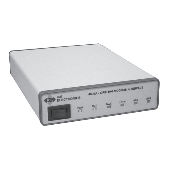
- Page 6 General Information INTRODUCTION This section provides the specifications for ICS's Model 4809A, 4819A 4829A and 4899A GPIB<->Modbus Interfaces and their accessory items. Models 4809A, 4819A and 4829A are PC board assemblies designed for mounting inside another piece of equipment. The Model 4899A is an en- closed Minibox™ product designed for bench top use with other equipment. All three products are functionally equivalent. The manual describes the units' functions by referring to the 4899A but, wherever the text refers to the Model 4899A, it also applies to the other models unless otherwise stated. Any model differences are noted in parenthesis or in separate paragraphs. DESCRIPTION The Model 4809A/4819A/4829A/4899A GPIB<->Modbus Interfaces are IEEE-488.2/GPIB to Serial Interfaces with special firmware to control Modbus RTU Slave devices from the GPIB or HP-IB bus. They let the user send simple commands with ASCII values over the GPIB bus to control and query slave Modbus devices. Each interface converts GPIB commands into the Modbus protocol and adds the CRC checksum to make a complete Modbus RTU message. The messages are sent serially over a RS-232 link or over a RS-485 network. Responses are checked and valid response data from a query is returned to the GPIB bus when the 4899A is next addressed to talk. The 4809A and 4899A handle both RS-232 and RS-485 Modbus devices. The 4819A handles only RS-232 devices while the 4829A handles...
- Page 7 Status Reporting Structure that complies with the SCPI standard. SCPI commands are used to set the unit's GPIB address, to set the serial configuration, and to enable bits in the Status Reporting Structure to generate SRQs. The user can also enter his own IDN message to personalize the unit as part of his assembly. All settings are saved in nonvolatile memory. The Model 4899A is packaged in a small Minibox™ metal case that is less than 1U in height (1.6 inches) The front panel contains the power switch and LEDs which indicate the unit's status. The rear panel contains the GPIB and serial connectors and a DC power jack. The 4899A accepts a wide range of DC voltages and is shipped with an adapter for the local power lines. The 4899A can be used as a stand-alone box or rack mounted inside a standard 19-inch wide equipment rack. The Model 4809A is a small, low-profile PC assembly designed for mount- ing inside the host chassis. It has two flat-ribbon connectors for its GPIB signals. One connector can be connected to a panel-mounted GPIB connector on a pin-to-pin basis. The second connector mates to one of ICS's GPIB Connector/Address Switch Assemblies which mount a GPIB connector and an GPIB address switch on the rear panel of the host chassis. ICS's GPIB Connector/Address Switch Assemblies are available in two mounting styles as described in Appendix 3. The RS-232 and RS-422 serial signals are available on a flat-ribbon header and on a DB-25P connector. The 4809A has the same status LEDs as the 4899A and runs on 5 to 12 volt power. The Model 4819A and 4829A are small PC assemblies with GPIB and RS- 232 serial interfaces. Both are designed to be mounted to the rear panel of the host chassis so the GPIB and external serial connectors protrude through the rear panel. Both interfaces can be used to control the internal Modbus device. The 4819A ORs the external serial input and the serial Modbus pack- ets generated by GPIB bus commands into a single-ended RS-232 signals to drive the internal Modbus device. Modbus device responses are available at either interface. The 4819A has the same diagnostic LEDs as the 4899A and runs on 5 to 12 volt power. The 4829A provides differential RS-422/RS-485 signals to drive multiple Modbus slave devices. The 4829A also includes...
- Page 8 MODEL 4809A/4819A/4829A/4899A SPECIFICATIONS The following specifications apply to all models. Options for your unit may be found by comparing the list below to those listed on the serial label on your unit. 4899A - X General Model Number Option Codes Special Crystal Custom Paint Custom Front Panel Special Program Factory Installed Rack Mount Kit Ship with Australian 230 Vac Adapter Ship with British 230 Vac Adapter Ship with European 230 Vac Adapter Base Model Number 4899A - Minibox Product 4809A - Board Product 114922 - 4809A board only version 4819A - Board Product 115122 - 4819A board only version 4829A - Board Product 115782 - 4829A board only version Note options -3, -5, -9, and the AC adapters do not apply to the Model 4809A or 4819A and to their board only versions. The 48x9A version interfaces have additional floating point Modbus com- mands not available in the original 48x9 interfaces. The 48x9A series units are fully compatible with the original 48x9 interfaces.
- Page 9 IEEE 488 INTERFACE 1.4.1 488.1 Capabilities The 488 Bus interface meets the IEEE STD 488.1-19A87 standard and has the following capabilities: SH1, AH1, T6, L3, SR1, PP0, DC1, RL0, DT0, C0 and E1/E2 drivers. 1.4.2 Address Ranges Primary addresses 0 - 30 1.4.3 Buffers GPIB input 2 kbytes GPIB output 1 kbytes Serial input/output 256 bytes 1.4.4 488.2 Common Commands The 4899A conforms to IEEE STD 488.2-19A87. When addressed to listen in the command mode, the unit responds to the following 488.2 commands: *CLS, *ESE, *ESE?, *ESR?, *IDN?, *OPC, *OPC?, *PSC *RCL, *RST, *SAV, *SRE, *SRE?, *STB, *TST?, and *WAI. 1.4.5 SCPI Parser The extended SCPI parser complies with the SCPI Standard Version 1994.0.
- Page 10 SERIAL MODBUS INTERFACE The 4899A and 4809A's serial Modbus interface provides RS-232 single- ended and RS-485 (RS-422) differential signals. Signals are selected by internal jumpers. The 4899A has a DB-25S connector on its rear panel, the 4809A has a 26-pin flat-ribbon header and a DB-25P connector. Signal pinouts conform to EIA RS-530 specification and are listed in Table 2-2. The 4819A provides RS-232 single-ended signals on a DE-9S connector. DCE/DTE jumpers let user exchange TX and RX signal pin numbers. Signal pinouts are listed in Table 2-3. The 4829A provides RS-422/RS-485 differential signal pairs on a DE-9S connector. On-board jumpers let user connect the TX and RX signal pairs together for 2-wire networks. The RX pair includes a termination network for biasing 2-wire networks. Signal pinouts are listed in Table 2-4. 1.5.1 Modbus RTU Messages Messages conform to the Modbus RTU format and include the device ad- dress, command, register number, data and CRC formatted as binary bytes. Supported Modbus commands are: 01, 02, 03, 04, 05, 06, 07, 08, and 16 for integer values and commands 03 and 16 for floating point 32-bit values. Integer range 16 bits or 0 to 65,536 Floating point IEEE-754 1.5.2 Baud Rates: Parser selects closest rate to specified rate when a nonstandard rate entered. Standard rates are: 50, 110, 300, 600, 1200, 2400, 4800, 7200, 9600, 14400, 19200, 28800, 38400, 57600, 76800 and 115200 baud. Baud Rates: 4899A - Any rate from 50 to 115,200 baud. 4809A - Any rate from 50 to 38,400 baud. 4819A - Any rate from 50 to 57,600 baud. 4829A - Any rate from 50 to 57,600 baud.
- Page 11 1.5.4 RS-232 Specifications Single-ended RS-232C drivers and receivers that are designed to operate with up to 50 feet of cable. Transmit +9 Vdc = Logic "0" or On Levels -9 Vdc = Logic "1" or Off Receive ±1.5 Vdc minimum, ±25 Vdc Maximum Signals 4899A AA, AB, BA, BB, CA, CB, CD and CF 4809A 4819A AA, AB, BA and BB CC held high, CA jumpered back to CB 1.5.5 RS-422/RS-485 Specifications The 4809A, 4829A and 4899A have differential RS-485 line drivers and receivers that provide RS-422 and RS-485 compatible signals. The line drivers and receivers are designed to operate with up to 1200 meters of twisted-pair cable. The transmitter can be set for continuous on for 4-wire systems or it can be tristated when not transmitting for 2-wire systems. Modes Transmitter on or tristated when not transmitting...
- Page 12 PROGRAMMABLE FUNCTIONS All units use IEEE 488.2 and SCPI commands to change their program- mable functions and jumpers to select the serial signals. Table 1-1 lists the programmable functions and their factory default settings. The 4899A and 4809A are factory set for RS-232 signals. The 4829A is factory set for 4-wire operation. TABLE 1-1 FACTORy CONFIGURATION Command Functions Factory Setting :ADDRess Sets GPIB bus address :EXT Enables External GPIB Address Switch OFF (4809A only) # :BAUD Sets transmit/receive baud rate 9600 # :PARity Sets parity type NONE # :CHECK Enables parity checking OFF # :BITs Sets number of data bits per character :SBITs Sets number of stop bits/per character :RS485 Tristate transmitter enabled OFF # :FORMat Sets talk format for response data ASCii # *ESE...
- Page 13 INDICATORS Six LEDs that display the following conditions: PWR - Indicates power on. RDY - Indicates unit has passed self test. TALK - Indicates unit has recognized its talk address. LSTN - Indicates unit has recognized its listen address. SRQ - On when the RQS bit is set. ERR - On when ESR bits 2 thru 6 are set on. When the 4899A is turned on, it performs an internal self test which takes about 0.5 seconds. Only the PWR indicator is on during self test. At the end of the self test the 4899A displays its current GPIB address by blinking the front panel LEDs for one-half second. The GPIB address is the sum of the binary bit weights. The LED bit weights are: RDY TALK LSTN SRQ Any errors found during self test are indicated by a repeated blinking of the error code pattern. Refer to paragraph 5.4 for a description of the selftest errors and their possible causes. During normal operation, the ERR LED indicates that there was a problem with the GPIB command or with the Modbus communication. If the ERR LED illuminates at power turn-on, it indicates that the unit has not been calibrated since the memory was last initialized. Refer to paragraph 5.3.1 for directions on calibrating the unit.
- Page 14 PHySICAL 1.8.1 4899A Minibox Size 7.45" L x 5.57" W x 1.52" H (18.92 cm L x 14.15 cm W x 3.86 cm H) (See Figure 1-1) Weight 3 lbs (1.4 kg) including adapter Temperature Operating -10 °C to +55 °C Storage -40 °C to +70 °C Humidity 0-90% RH without condensation Shock/Vibration Normal handling only Construction All metal case Power 9 to 32 Vdc @ 3.5 VA Connectors IEEE 488 Interface Amphenol 57-20240 with metric studs Serial Interface Cinch DB-25S female connector with lock studs...
- Page 15 Figure 1-1 4899A Outline Dimensions 1-10...
- Page 16 1.8.2 4809A Board Assembly Size 5.50" L x 4.50" W x 0.5" H (139.7 mm L x 114.3 mm W x 12.7 mm H) (See Figure 1-2) Weight 6 oz. (0.17 kg) Temperature Operating -10 °C to +55 °C Storage -40 °C to +70 °C Humidity 0-90% RH without condensation Shock/Vibration Normal handling only Construction Flame-retardant printed circuit board Power 5 ± 0.25 Vdc @ 300 MA (regulated) 5.5 to 12 Vdc (unregulated) Connectors GPIB - 24-pin 3M 2524 male header GPIB/Address Sw - 26-pin 3M 2526 male header Serial - 26-pin 3M 2526 male header and DB-25P male connector. 1-11...
- Page 17 0.150 dia hole 0.300 clear pad GPIB 0.200 8 plcs 4809A 4.500 Serial I/O FULL 5.500 Figure 1-2 4809A Outline Dimensions 4.00 0.20 typ. 0.50 typ. Status LEDs GPIB Connector 4819A 4.50 4829A Serial Device Connector Serial Connector 0.190 dia mounting holes (4 plcs) 0.300 dia mounting pads...
- Page 18 1.8.3 4819A and 4829A PHySICAL Size 4.00" L x 4.50" W x 0.7" H (10.16 cm L x 11.43 cm W x 1.78 cm H) (See Figure 1-3) Weight 8 oz (0.22 kg) Temperature Operating -10 °C to +55 °C Storage -20 °C to +70 °C Humidity 0-90% RH without condensation Shock/Vibration Normal handling only Construction Flame-retardant printed circuit board. Connector shells grounded to chassis supports and mounting brackets. Power 5 ± 0.25 Vdc @ 300 MA (regulated) 5.5 to 12 Vdc (unregulated) Connectors GPIB - 24-pin IEEE-488 connector with metric studs External RS-232 Interface - DE-9S male connector with lock studs Internal Serial Interface - DE-9P female connector with lock studs 1-13...
- Page 19 4899A CERTIFICATIONS OR APPROVALS EMI/RFI Meets limits for part 15, Class A of US FCC Docket 20780 and complies with EEC Standards EN 55022 and 50082-1. CE Certificate of Compliance reproduced in Figure 1-4. UL/CSA/VDE AC Wall adapter has applicable UL/CSA/VDE and CE approvals 1-14...
- Page 20 Certificate of Conformity Application of Council Directives ........89/336/EEC Standard(s) to which Conformity is Declared ..EN 55022, EN50082- Manufacturer's Name ICS Electronics div Systems West, Inc. Manufacturer's Address 473 Los Coches Street Milpitas, CA 95035 Importer's Name Importer's Address Type of equipment GPIB to Serial Converter Model No. 4899 1999 Serial No. Thru , Year of manufacturer I, the undersigned, hereby declare that the equipment specified above con- forms to the above Directive(s) and Standard(s) by virtue of its similarity with the Model 4894.
- Page 21 Horizontal GPIB Connector/Address Switch Assembly (Dash number is cable length from 10 to 90 CM long. 90 CM standard) 113642-L Vertical GPIB Connector/Address Switch A ssembly (Dash number is cable length from 10 to 90 CM long. 90 CM standard) 114439-L GPIB Flat Ribbon Extension Cable for 4809A. (Dash number is cable length from 10 to 90 CM long. 90 CM standard) 114256-L Serial Flat Ribbon Extension Cable from 4809A to DB- 25P male connector. (Dash number is cable length from 10 to 90 CM long. 90 CM standard) 1-16...
- Page 22 Installation UNPACKING When unpacking, check the unit(s) for signs of shipping damage (damaged box, scratches, dents, etc.) If the unit is damaged or fails to meet specifica- tions, notify ICS Electronics or your local sales representative immediately. Also, call the carrier immediately and retain the shipping carton and pack- ing material for the carrier's inspection. ICS will make arrangements for the unit to be repaired or replaced without waiting for the claim against the carrier to be settled. SHIPMENT VERIFICATION Take a moment to verify the shipment. Each shipment includes: (1) Model 4809A, 4819A, 4829A or 4899A GPIB<->Modbus Interface (1) AC Power Adapter (Model 4899A only) (1) 4809A/4819A/4829A/4899A Instruction Manual (1) Support CD-ROM Board only orders do not include manuals or configuration disks unless ordered separately. Take a moment to check ICS's website at http://www.icselect.com for any manual errata or the latest configuration programs.
- Page 23 INSTALLATION GUIDES 2.3.1 4899A Installation Guide The following steps should be used as a guide to setting up and using your 4899A. 1. If the 4899A is to be used with RS-422 or RS-485 signals, change the jumper settings as directed in Section 2.11. 2. See Section 2.10 to select and/or design the serial cable. CAUTION - Check 'standard' serial cable wiring carefully as may standard cables may not make proper connections to the Modbus RTU Controller. 3. If the unit is to go into a rack mounting kit, disconnect all cables from the unit. Follow the instructions in Section 2.12 to install the unit it in the rack mounting kit. 4. Connect the AC adapter to the 4899A and to the AC power. Turn the unit on and verify that it passes its selftest and that it indicates the correct GPIB address. Use the *IDN? query to verify GPIB communication. 5. Review the factory settings in Table 1-1 to determine if your unit needs to be reconfigured. If the 4899A needs to be reconfigured, follow the instructions in Sections 2.4 - 2.8 to change its configura- tion. Save the new settings. 6. Use a GPIB keyboard or similar interactive GPIB control program to query the internal modbus device's model number or some other known value following the examples in section 3.8. A typical message would be 'R? 0,1' to query its model number. Read the response to confirm that it is the expected response. Try out other Modbus commands that apply to the Modbus device.
- Page 24 4809A Installation Guide The following steps should be used as a guide to the 4809A installation. 1. If the 4809A is to be used with RS-422 or RS-485 signals, change the jumper settings as directed in Section 2.11. 2. Review Sections 2.8 and 2.10 to select and/or design the GPIB and serial interface cables. 3. Select a convenient location to mount the 4809A. Do not mount it directly over a heat producing surface. Provide a 0.1 inch (2.5 mm) clearance underneath the 4809A or use an insulator if the 4809A is being mounted on a metal surface. Use the dimensions in Figure 1-3 to establish the mounting hole locations. 4. Use a twisted pair of #24 wires to connect the 4809A's power terminals to the host's power supply. Connect the 4809A directly to the power supply to avoid noise problems. Set jumper W1 to REG for unregulated 5.5-12 volt power, to P1 for regulated 5 volt power. 5. Plug in the GPIB and serial cables and connect the unit to the GPIB controller. Turn the unit on and verify that it passes its selftest and indicates the correct GPIB address. Use the *IDN? query to verify GPIB communication. 6. Review the factory settings in Table 1-1 to determine if your unit needs to be reconfigured. If the 4809A needs to be reconfigured, follow the instructions in Sections 2.4 - 2.8 to change its configura-...
- Page 25 2.3.3 4819A/4829A Installation Guide The following steps should be used as a guide to the 4819A or 4829A installation. 1. Review Section 2.10 to select and/or design the serial interface cables. 2. Select a spot on the rear panel to mount the board. The 4819A/4829A mounts perpendicular to the rear panel and is held in place with mounting blocks. Use the cutouts and mounting dimensions shown in Figure 2-1 for the connector cutouts. Cutout 'A' is for the IEEE- 488/GPIB connector. Cutout 'B' is for the DE-9 serial connector. Do not mount the board directly over a heat emitting surface. Pro- vide a 0.1 inch (2.5 mm) clearance underneath the board or use an insulator if the board is being mounted on a metal surface. 0.320 0.247 0.218...
- Page 26 supply to avoid noise problems. Set jumper W2 to REG for un- regulated 5.5 -12 volt power, to P1 for regulated 5 volt power. 5. Plug the cable from the internal modbus device into J3 and connect the board to a GPIB controller. Turn the unit on and verify that it passes its selftest and blinks its correct GPIB address. Use the *IDN? query to verify GPIB communication with the board. 6. Review the factory settings in Table 1-1 to determine if your unit needs to be reconfigured before it can send data to the serial device. If the board needs to be reconfigured, follow the instructions in Sections 2.4 - 2.8 to change its settings. Save the new values. 7. Use a GPIB keyboard or similar interactive GPIB control program to query the internal modbus device's model number or some other known value following the examples in section 3.8. A typical message would be 'R? 0,1' to query its model number. Read the response to confirm that it is the expected response. Try out other Modbus commands that apply to the Modbus device.
- Page 27 CONFIGURATION DIRECTIONS When shipped, the 4809A, 4819A, 4829A or 4899A are set to the factory configuration listed in Table 1-1. The configurable parameters are stored in Flash (EEPROM memory on older boards) and can be queried and changed by the user. Configuring a 4899A is a three step process. First design the link between the unit and the serial device. This will provide you with the serial configuration values. Secondly, review the SCPI commands and programming guide in Section 3 to select the configuration settings. Then follow the instructions in 2.6 or 2.7 to configure the unit. If you are using a PC as a bus controller, the easiest way to configure the unit is to use ICS’s Minibox configuration program, niconf_w.exe, which guides the user through a menu-driven configuration procedure. niconf_w.exe runs with any ICS, National Instruments, MCC or other GPIB Controller card that has a GPIB-32.DLL and uses the NI command set. Follow the instructions in Section 2.6 when using the niconf_w.exe configuration program. Because these units have only a few configurable parameters, they can be easily configured by entering the SCPI commands directly into an interac- tive command line utility supplied by your GPIB Controller Card manufac- turer. You can also use ICS’s GPIBkybd program with any Adlink, ICS, Keithley, MCC or National Instrument GPIB Controller card. Follow the instructions in Section 2.7 when using one of these interactive command line programs.
- Page 28 THE SUPPORT CD-ROM The Support CD-ROM contains Configuration Programs, Utility Programs, and Example Programs for ICS’s interface products plus backup Manuals Application Notes and reference materials. When you load the CD into the CD-ROM drive, it should automatically run and display the Support CD Selection Window. Click Configure GPIB Interfaces to run the niconf_w.exe program or Install Keyboard Utilities to install the GPIBkybd program. You can always download niconf_w.exe from the Support CD and save it on your hard drive and later run it directly from our hard drive. CAUTION Do not click on Install 488.2V3 Driver as that may damage your existing GPIB Driver Installation. Use the Browse CD or View Readme File to examine the CD contents.
- Page 29 GPIB Bus Cable 4899A AC Adapter (a) 4899A Configuration Setup Connect the 4809A, 4819A or 4829A to the GPIB controller card in the PC or to a USB-GPIB Controller as shown in Figure 2-2(b). Connect a DC power supply to the power terminal strip. Set jumper W2 to the P1 position. Set the power supply to 5 ± 0.2 Vdc. PC with GPIB Controller Card DC Power Supply GPIB Bus Cable 4819A (b) 4809A , 4819A or 4829A Configuration Setup Figure 2-2 Configuration Setups 2. Apply power to the unit. After 0.5 seconds, the unit should blink its GPIB bus address on the LEDs. The selftest ends with the PWR and RDY LEDs both on and the other LEDs off.
- Page 30 3. Run the configuration program. This may be done by double click- ing on the program name or by typing the program's name at the DOS prompt or in the Windows Run command box. > c:\new_directory\MCONFIG <return> 4. Product Selection The program will display a list of model numbers. Enter or select the number that corresponds to the model that you are configuring and press return 4899A <return> 'selects Model 4899A The program may ask that you turn the unit off and back on. Press the Continue key when the unit has finished its self test. 5. GPIB Address The program branches to the selected product menu and asks for the unit's current GPIB address. Enter a one or two digit value ; i.e., 4, 04, 10 and click the SET button. The factory default set- ting is 4. If you do not know the unit's GPIB address, turn the unit off and back on. The unit will blink its GPIB address on the front panel LEDs at power turn-on. Add the bit weights to get the GPIB address. RDY TALK LSTN SRQ ERR 16 8 4 2 1 Configuration Choices The configuration program steps through each parameter and dis- plays the current setting and configuration choices. The user should refer to the command definitions in Table 3-3 to understand the command choices and their affect on the unit’s operation. Setting changes are made by entering a value in the box above the Enter/...
- Page 31 Figure 2-3 Configuration Program shown prior to saving the new settings Saving the New Settings After the last parameter has been accepted, the program will give you several configuration choices. The program may give you the opportunity to set the SRE and ESE enable bit registers and to save the values so the unit can generate a SRQ at power turn-on. Enter y to set PSC 0; N to set PSC 1 or click the appropriate boxes. The program may ask if you want to lock the parameters so that they cannot be changed by the end user. The configuration program automatically unlocks the parameters whenever it is run. Enter y to lock; N to continue or click the appropriate box. The program will ask if you want to save the current configuration. Enter y to save; N to continue or click the appropriate box Configuring other units The program will ask if you want to configure another unit. Enter y to configure another unit; N to exit. 2-10...
- Page 32 CONFIGURING WITH AN INTERACTIVE PROGRAM 2.7.1 General Configuration Instructions The 4899A can be easily configured from any GPIB bus controller with an interactive program such as ICS's GPIBkybd program by using the fol- lowing procedure. Connect the unit to the GPIB controller as shown in Figure 2-2. Run the program and if required use an Abort, REN or a take control type command to have the bus controller assert REN. Then turn the unit on. Determine the unit’s GPIB address: For new units use the factory setting of 04. For other units, turn the unit off and back on. At the end of its self test, the unit blinks its GPIB address on the LEDs. TALK LSTN SRQ Figure 2-4 GPIBkybd Program with 4829A's IDN response 2-11...
- Page 33 Verify communication to the unit by sending it the *IDN? query and reading back the unit’s IDN message. GPIBkybd users can use the pulldown arrow on the right side of the Device Command window and select *IDN?. Use the SCPI Command tree in Table 3-2 to put together the SCPI command for the parameter you want to change. (See paragraph 3.6 if you need help using SCPI commands.) Enter the commands into your interactive program (GPIBkybd Device Command Window) and press “Send”. If you are querying a value press the “Query” if the program has that choice. If not, you will have to manually “Read” the response. ICS’s GPIBkybd program has an auto query function so it will automatically read back a response if you just press “Send”. The following example shows how to change and query the baud rate. SYST:COMM:SER:BAUD 19200 ‘sets the baud rate SYST:COMM:SER:BAUD? ‘queries the baud rate ‘should reply 19200 Use caution when changing the unit’s GPIB address. The change takes place immediately when the command is executed. Provide a 0.1 second delay before querying the new address setting. i.e., to change the GPIB address to 20 SYST:COMM:GPIB:ADDR 20 ‘ send address 20 ‘Wait 0.1 seconds Change the device’s GPIB address in the interactive program to the new address, in this case 20. Query the device to be sure the address changed.
- Page 34 GPIB CONNECTIONS 2.8.1 4819A, 4829A and 4899A GPIB Connections The 4819A, 4829A and 4899A have standard 24-pin IEEE-488 connector with metric lock studs. Their IEEE-488 connector mates with all stan- dard IEEE 488/GPIB bus cables. Signal-pin assignments for the standard IEEE-488 connector are shown in Figure A-2 in the Appendix.2.9 2.8.2 4809A GPIB Connections The 4809A has two male flat-ribbon male connectors that can be used to connect the 4809A to the GPIB bus. Connector J1 is a 24-pin connector that is designed for pin-to-pin connection to the GPIB. Connector J2 is a 26-pin connector that contains the address switch input signals and the GPIB bus signals. The 4809A only requires that one of the connectors be used to connect it to the GPIB bus. The unused connector should be left open. 2.8.2.1 GPIB Connector J1 The GPIB Signal-pin assignments for J1 are identical to a standard IEEE-488 connector as shown in Figure A-2 in the Appendix. The J1 connector layout is shown in Figure 2-5. Use a flat ribbon cable like ICS’s 114439-L cable with a 24-pin plug on one end and a GPIB connector on the other end to connect J1 to the GPIB bus. Cut an opening for the GPIB connector on the rear panel (See cutout A and holes C in Figure 2-1). Mount the GPIB connector on the rear panel of the chassis with the metric lockstuds. Fab- ricate a flat ribbon cable as shown in Figure 2-6 or purchase it from ICS Electronics as P/N 114439-L where L is the cable length in cm. Board Figure 2-5 Edge...
- Page 35 2.8.1.2 GPIB/Address Switch Connector J2 Connector J2 is a 26-pin connector that contains the GPIB external address switch signals as well as the GPIB bus signals. J2 is used when you want to use an external GPIB address switch with the 4809A. The J2 connector layout is shown in Figure 2-8 and the signal-pin assignments are listed in Table 2-1. The external address switch inputs are low true signals with pullup resistors on the 4809A. At power turn-on, the 4809A reads the five address lines (ADSW1-ADSW5) if the external address switch is enabled. Connector J2 mates with ICS’s GPIB Connector/Address Switch Assem- blies. These assemblies are small business card size assemblies that mount a GPIB connector and a 8-bit rocker switch to the rear panel of a chassis. They have a 26 conductor, flat ribbon cable that plugs into J2 on the 4809A. The assemblies are available in two layout styles. Refer to Appendix A3 for dimensions, installation instructions and silkscreen. Switch layout and rocker functions are shown in Figure 2.7. Note that rockers 7 and 8 are not used by the 4809A. Switch set to address 4 On is up 2 3 4 1 8 4 2 1 0 - - Figure 2-7 Address Switch Rocker Assignments...
- Page 36 TABLE 2-1 4809A GPIB/Address Connector Signals (J2) Signal Wire Number Color Weights GROUND BRN 1 ADSW5 RED 1 16 (MSB) T SW ORG 1 not used L SW YEL 1 not used ADSW4 GRN 1 SI SW BLU 1 not used ADSW1 VIO 1 1 (LSB) ADSW3 GRY 1 ADSW2 WHT 1 NRFD BLK 1 GPIB Signals REN BRN2...
- Page 37 SERIAL INTERFACE CONNECTIONS 2.9.1 4809A Serial Connections The 4809A’s serial port is a DTE (Data Terminal Equipment) interface on a 26-pin male ribbon connector (J3) and a DB-25P connector (J4). The 26-pin male ribbon connector is for compatibility with the earlier 4809’s. The DB-25P connector allows standard DB-25S connectors to be used with the 4809A. RS-232 and RS-422 (RS-485) signal selection is made by setting jumpers on the 4809A. Refer to section 2.13 for jumper setting instructions. Table 2-2 shows the 4809A’s signal-pin assignments and signal directions. Figure 2-9 shows the pin layout for connector J3. 2.9.1.1 4809A LED Outputs The 4809A’s TALK and LSTN LED driver outputs are provided on pins 17 and 21 on connector J3 and J4 to drive remote LEDs. Each signal is low true and can sink 3 mA. Use a resistor in series with 5 Vdc to limit the current to LED. Connect the LED cathodes to the driver signals. The recommended resistor value is 1500 ohms for 5 Vdc. Connect the 5 volt return line to pin 7. 2.9.2 4819A Serial Connections The 4819A has two right-angle 9-pin connectors for its RS-232 interfaces. Connector J2 is the external serial connector that protrudes through the rear panel. Connector J3 is the internal serial connector for connecting the...
- Page 38 RR(A) Signal Detected (A) ← RR(B) Signal Detected (B) ← CS(B) Clear-to-send (B) ← SD(B) Send Data (B) → RD(B) Receive Data (B) ← 4809A Talk LED Dvr- → RS(B) Request-to-send (B) → TR(A) Data Terminal Rdy (A) → 4809A Listen LED Dvr - → TR(B) Data Terminal Rdy (B) → Note: Pin 26 is only available on the 4809A Board Edge Figure 2-9 4809A J3 Serial Connector Pin Layout 2-17...
- Page 39 TABLE 2-3 4819A SIGNAL ASSIGNMENTS Rear Panel Connector J2 Internal Connector J3 Pin # Signals Signal Signals Pin # DE-9P Direction DE-9S DCD DCD TxD TxD * ← RxD RxD * → DTR +V DTR GND GND − DSR DSR RTS +V RTS CTS CTS...
- Page 40 TABLE 2-4 4829A SIGNAL ASSIGNMENTS Rear Panel Connector J2 Internal Connector J3 Pin # Signals Signal Signals Pin # DE-9P Direction DE-9S DCD RD(B) TxD RD(A) ← RxD SD(A) → DTR +V SD(B) GND GND − DSR RTS +V CTS −...
- Page 41 4819A are wired to some typical RS-232 Temperature Controllers. Refer to Table 5-2 for troubleshooting Modbus Device communication problems. Figure 2-10 shows the 4899A or 4809A RS-232 connection to a Watlow F4 Temperature Controller. Both interfaces transmit on pin 2 and receive on pin 3. WATLOW F4 4899A/4809A 4899A 4809A Figure 2-10 4899A/4809A RS-232 Connections to a Watlow F4 Figure 2-11 shows the 4819A's RS-232 connection to a Watlow F4 Tem- perature Controller. The 4819A's transmit signal is on pin 3 and its receive input signal is on pin 2 with the DCE/DTE jumpers W4 set in the DCE position. Switch jumper W4 to the DTE direction to swap the signal pin assignments. WATLOW F4 GPIB 4819A 4819A Serial...
- Page 42 Figure 2-12 shows the 4819A's RS-232 connection to a Watlow series 96 Temperature Controller. WATLOW GPIB 4819A 4819A Serial Figure 2-12 4819A RS-232 Connections to a Watlow 96 2.10.2 RS-485 Connections to a Modbus Device The 4809A, 4829A and 4899A's serial interface provides a transmit (SD) and a receive (RD) pair of RS-422/RS-485 signals. Because most RS-485 Modbus networks are two wire, half-duplex networks, the SD and RD sig- nal pairs have to be jumpered together in the cable connector. The 4809A, 4829A and 4899A have to be configured for RS-485 operation when used on a two wire RS-485 network. Use the SYST:COMM:SER:RS485 ON command to configure the units. The ON setting causes the unit to tristate its serial transmitter when not transmitting which free's the network so the Modbus can respond to the message. Two wire RS-485 networks also need termination networks to bias the lines in the 'mark' state when neither unit is transmitting. The termination networks are made up of a pullup, a pulldown and a load resistor. The termination networks prevent each receiver from inputting noise when nothing is being transmitted. Use one termination network for short cables of 200 feet or less. For longer cables, use a termination network at each end of the cable. Set the bias voltages to approximately 2 Vdc and 2.5 Vdc. Use resistors with an approximate value of 500 ohms/volt.
- Page 43 4899A or 4809A DB-25P Tx/Rx- SD(A) Tx/Rx+ SD(B) RD(A) RD(B) Figure 2-13 4899A/4809A Pullup/Pulldown Resistor Connections Figure 2-14 shows an example of a single 4899A or 4809A driving two Modbus devices over a RS-485 network. In Figure 2-12, the termination network uses 5 Vdc and ground provided by the Watlow F4 Temperature Controllers. WATLOW F4 T+/R+ 4899A T-/R- 4809A WATLOW F4 Figure 2-14 RS-485 Network connections to Watlow F4 Controllers Figure 2-15 shows an example of a single 4899A or 4809A driving a Watlow EZ Zone Controller with a simple point-to-point RS-485 network. The EZ Zone controller does not have easy terminals to attach a termination network so the network connections shown in Figure 11 are reused here.
- Page 44 The 4899A/4809A's internal pullup resistor at pin 20 is used to pullup the SD(B) and RD(B) lines and apply a positive signal to the Tx/Rx- line. A 1 kohm resistor from SD(A) and RD(A) to ground is the pulldown resistor for the Tx/Rx+ line. The 220 ohm load resistor completes the circuit. 4899A/4809A AC Power DB-25P Tx/Rx- SD(A) Tx/Rx+ RD(A) SD(B) RD(B) +5 V Figure 2-15 RS-485 Network connections to a Watlow EZ Zone Controller Figure 16 shows an 4829A driving a single Watlow EZ Zone Controller with it RS-485 output. The 4829A has an internal termination network with a 220 ohm load resistor so it does not need external resistors. If the internal W4 and W5 jumppers are installed (the gray links in Figure 2-16), then no external jumpers are required and the EXZ Zone Controler can be connected to either (A)-(B) signal pair. 4829A DE-9S AC Power RD(B) GPIB RD(A)
- Page 45 TABLE 2-5 4809A JUMPER SETTINGS Jumper Function Factory Setting Selects input power P1 for direct regulated 5 Vdc power REG for unregulated DC power Set for EPROM size. Not user changeable. Write Enable. Installed enables saving setup parameters Installed in EEPROM. Remove to block writes to configuration tables RS-232/RS-422 signal selection Jumpers 232* 232 for RS-232 signals 232* 422 for RS-422 signals Notes: * Set RS485 to 1 for half-duplex operation or to 0 for full-duplex operation. GPIB 256 512 Serial I/O BSY/ FULL/ Figure 2-17 4809A W4 and W5 Jumpers set to RS-422 Position 2-24...
- Page 46 2.11.2 4819A Jumper Settings The 4819A has five jumpers as shown in Figure 2-18. Table 2-6 lists the 4819A jumper functions and their factory settings. TABLE 2-6 4819A JUMPER SETTINGS Jumper Functions Factory Setting Write Enable - Must be in place to write to or to save Installed data in the 4819A’s flash memory. Power Selection - Selects input power. P1 position selects the terminal block for a 5 Vdc regulated power source. REG selects the regulator output for 5.5 to 15 Vdc power. Default - Install and power cycle the unit to reset the unit to Omitted its factory default settings. Leave out for normal operation. TxD/RxD Signal Swapping Jumper Pair - W4 can be used to swap the TxD/RxD pins on connector J3. Factory setting is the DCE position with the pinouts listed in Table 2-2. Jumpers GPIB logic ground to chassis ground. Omitted +P1- TALK LSTN GPIB 4819A Chassis Rear Panel Internal Serial I/O Serial I/O Figure 2-18 4819A Jumper Locations 2-25...
- Page 47 2.11.3 4829A Jumper Settings The 4829A has seven jumpers as shown in Figure 2-19. Table 2-7 lists the 4829A jumper functions and their factory settings. TABLE 2-7 4829A JUMPER SETTINGS Jumper Functions Factory Setting Write Enable - Must be in place to write to or to save Installed data in the 4819A’s flash memory. Power Selection - Selects input power. P1 position selects the terminal block for a 5 Vdc regulated power source. REG selects the regulator output for 5.5 to 15 Vdc power. Default - Install and power cycle the unit to reset the unit to Omitted its factory default settings. Leave out for normal operation. Connects SD pair to RD signal pair. Install for half-duplex Open* operation, omit for full-duplex operation. Enables RD transceiver 100% of time (Full-duplex) or only Full* when transmitting (Half-duplex operation) Jumpers GPIB logic ground to chassis ground. Omitted Notes: * Set the RS485 setting to match your jumper setting. +P1- TALK LSTN GPIB 4829A Chassis Gnd Full Half Internal Rear Panel...
- Page 48 2.11.4 4899A Jumper Settings The 4899A has internal jumpers for selecting RS-232 and RS-422/RS-485 signals. Figure 2-19 on the next page shows the jumper locations on the 4899A’s PC board. Table 2-8 lists the jumper functions. The jumpers are accessed by removing the two screws on the rear panel and sliding the unit out from the rear of its case. Jumpers W4, W5 and W6 select the type of signals for the 4899A’s serial interface. For RS-232 serial signals, leave the jumpers in the ‘232’ position as shown in Figure 2-15. For RS-422 or RS-485 signals, set jumpers W4, W5 and W6 to the ‘422’ position. Do not change the other jumper positions. Carefully slide the unit back into its case, fitting the PC board into the tracks on each side of the case. Be sure the switch and LEDs are correctly aligned before pushing the switch through the front panel. Replace the two rear panel screws. TABLE 2-8 4899A JUMPER SETTINGS Jumper Function Factory Setting Selects interrupt source CT/CV CT/CV for 4899A and 4895, PRL for 4892 Set for EPROM size. Not user changeable Write Enable. Installed enables saving setup parameters Installed in EEPROM. Remove to block writes to configuration tables RS-232/RS-422 signal selection Jumpers 232* 232 for RS-232 signals 232* 422 for RS-422 signals 232* LED signal jumpers CV/PRL for 4899A, CT for 4895...
- Page 49 DEFAULT Serial GPIB Figure 2-20 4899A Jumper Locations 2-28...
- Page 50 2.12 4899A RACK MOUNTING INSTRUCTIONS The Model 4899A is held in its rack mounting kit with a winged-'U' shaped bracket. Perform the following steps to install a 4899A in a rack mount- ing kit: Hold the 4899A at a 30 degree nose down angle and place the front bezel through the rack mount kit from the rear of the kit. Push it forward through the opening until the rubber feet line up with the holes in the rack mounting kit. Push the unit down until it rests flat on the kit and the feet are in the four holes. 2. Repeat step 1 for a second unit if two units are being held in one rack mounting kit. A line the unit(s) so the bezels are parallel with the front of the rack mount kit and protrude equally through the front panel of the rack mounting kit. Set the bracket so its two holes line up with the holes in the rack mounting kit extrusion. Use the supplied 4-40 screws to hold the bracket to the extrusion. Do not overtighten. 5. Use the supplied 10-32 screws to bolt the rack mounting kit into the rack. 2-29...
- Page 51 This page left intentionally blank 2-30...
- Page 52 Operation INTRODUCTION This section describes how the 4809A, 4819A, 4829A and 4899A interfaces operate and how they control Modbus RTU controllers from the GPIB bus. This section also describes the SCPI commands used to configure and control the units. Wherever the text refers to the Model 4899A, it applies equally to the Models 4809A, 4819A, and 4829A unless otherwise noted. OPERATION 3.2.1 Basic Operation The 4899A is a GPIB-to-Serial Interface with special firmware that converts GPIB commands into Modbus RTU packets to communicate with Modus devices. The 4899A responds to three types of commands: 1. IEEE-488.2 Common Commands in Table 3-2. These include the *IDN? and *ESR? queries and the *SAV 0 save command. 2. SCPI Commands in Table 3-3 are for setting internal values such as the GPIB address, serial parameters like baud rate and configuring the Status Reporting Structure. 3. Modbus Commands in Table 3-5 for communicating with Modbus device(s), setting the 4899A's serial timeout and reading the Modbus Error Register.
- Page 53 Communication with the Modbus device is serial and requires that the user set the 4899A and the Modbus device to the same serial settings. Each Modbus device has its own address so that it can respond to serial packets sent to its address. The Modbus device address is different and independent from the 4899A's GPIB bus address setting. Although the typical Temperature Chamber has only one Modbus Controller, the 4899A can drive multiple Modbus devices when using a RS-485 network. The 'C' command is used to set the Modbus device address in the 4899A. The 4899A remembers the Modbus device address until changed by a subsequent 'C' command or the 4899A is powered off or reset. Modbus devices are register based devices and they are controlled by writing values to registers that control different functions i.e. temperature setpoint, alarm settings etc. Data is taken from Modbus devices by reading registers associated with those parameters i.e. temperature, humidity, etc. ICS has created a set of simple Modbus commands for reading, writing and com- municating with Modbus devices. When these Modbus commands are sent to the 4899A over the GPIB bus, the 4899A communicates with the selected Modbus device. Modbus commands should not be mixed or concatenated with IEEE-488.2 or SCPI commands. If the 4899A's message packet is successfully received by the Modbus device, the Modbus device will generate a response packet that either confirms receipt of the message or that contains the requested data. The 4899A receives the response packet and validates the packet. If the response...
- Page 54 Service Request by asserting the SRQ line. The SRQ line stays asserted until the 4899A is serial polled or until the bits that caused the SRQ are reset. 3.2.2 4809A Differences The 4809A is a 4.5 by 5.5 inch board that mounts inside a chassis or tem- perature chamber. It is functionally identical to the 4899A and has both RS-232 and RS-422/RS-485 serial interfaces. The 4809A's baud rate is limited to 38,400 baud. 3.2.3 4819A Differences The 4819A mounts on the rear panel and has both a GPIB and an external serial connector which extends the Modbus serial path to the rear panel of the host chassis. The user can control an RS-232 Modbus device from the serial connector or from the 4819A’s GPIB interface. However, both interfaces cannot be used at the same time. Once the GPIB interface is activated, the serial interface cannot be used to control the Modbus device until the 4819A has been powered off and back on. 3.2.4 4829A Differences Like the 4819A, the 4829A mounts on the rear panel of the host chassis and has both a GPIB and an external RS-232 serial connector which extends the Modbus serial path to the rear panel of the host chassis. The user can control one to several RS-485 Modbus device(s) from the serial connec- tor or from the 4829A’s GPIB interface. However, both interfaces cannot be used at the same time. Once the GPIB interface is activated, the serial interface cannot be used to control the Modbus device until the GPIB con- nection is removed. ADDRESSING THE UNITS...
- Page 55 The internal GPIB address can be set or queried with the SCPI SYST:COMM: GPIB:ADDR command. The change takes affect when the command is executed so any subsequent commands will need to address the unit at its new address. Use the IEEE-488.2 common command *SAV 0 to save the new address value in the unit’s nonvolatile memory. Refer to Sections 2.6 and 2.7 for address setting instructions. 3.3.2 4809A Address External Address Switch The 4809A’s GPIB address can also be set by connecting the 4809A to an external address switch. Connector J2 contains the external address switch input lines in addition to the GPIB bus signals. J2 mates to ICS’s GPIB Connector/Address Switch Assemblies. These assemblies are small busi- ness card size assemblies that make it easy to mount a GPIB connector and an address switch on the rear panel of the host chassis. The 4809A’s external address switch is enabled with the SCPI SYST:COMM: GPIB:ADDR:EXT ON command. When enabled, the 4809A reads the external address switch at power turn-on. If the address switch is changed, the unit must be powered off and back on before it will respond to the new address. When the external address switch is enabled, the internal address value is ignored. 488.2 STATUS REPORTING STRUCTURE...
- Page 56 The 4899A includes the expanded IEEE-488.2 status reporting structure shown in Figure 3-1. The expanded status reporting structure conforms to the SCPI 1994.0 Specification and builds on the IEEE 488.2 Standard status structure with the addition of the Questionable, Operation and Modbus Error registers. The Event and Status registers are controlled and queried with the IEEE-488.2 common commands. The Status Byte Register may also be read by serial polling the 4899A. The added Questionable and Operation registers are controlled and queried with SCPI commands. The Modbus Error register is read and cleared with the Modbus E? command. As shown in Figure 3-1, IEEE 488.2 SRQ generation is a multilevel function and is determined by the occurrence of an event that has its corresponding enable bit set to ‘1’. The register outputs are summarized in the Status Byte Register which generates the Service Request and pulls the SRQ line low. SRQs are used to signal the bus controller that an event has occurred and/or that the 4899A needs service. There are four major sources of SRQs, each of which is summarized in a bit in the Status Byte Register. Three of the sources are event registers with their own enabling bits and the fourth is the Output Queue. The Event registers and the Output Queue are cleared when read or by the *CLS command. 3.4.1 Event Registers An event register captures 0 to 1 transitions in its associated condition register or in the standard event register. An event bit becomes TRUE (1) when the associated condition bit makes logical 0 to 1 transition. Once an event bit is set it is held until the event register is read or cleared with the *CLS command. Each event register contains eight or sixteen bits. When the register is read, its response is a decimal number that is the sum of the binary bit weights of the bits that are logical 1s. e.g., 23 decimal = 0001 0111 or 0000 0000 0001 0111 binary Each event register bit has a corresponding enable bit. The enabling bits are ANDed with the state of the event bits to create the summary condition in the Status Byte Register. Unwanted conditions can be blocked from generating SRQs by setting their corresponding enabling bit to a ‘0’. The...
- Page 57 Modbus Error Register Standard Event Status Register 7 6 5 4 3 2 1 0 *ESR? Queue Not-Empty & & & & & & Standard & Event Status & Enable Output Queue Register 7 6 5 4 3 2 1 0 *ESE <NRf>...
- Page 58 enabling bits are set by writing the value equal to the sum of all of the desired logic 1 bits to the enabling register. The value is normally decimal but can be expressed in HEX, OCTAL or BINARY by prefixing the number with a #H, #O or #B. 3.4.2 Event Status Register The Event Status Register reports events that are common to all 488.2 devices. This includes events such as self test errors, command errors, execution errors, power on and operation complete. ESR bits 2 through 6 light the ERR LED when on. The Power-on event occurs at power turn-on and can be used to signal a power off-on occurrence. In the 4899A, the Modbus Error Register is summarized into the Event Status Register as Bit 6. The 488.2 Operation Complete event has no meaning for either unit. TABLE 3-1 ESR BIT DEFINITIONS Event Description Weight 128 PON The Power-on event occurs at power turn-on and can be used to signal a power off-on occurrence. Modbus Modbus Error detected. Reading the Modbus Errror Register Error clears this bit. See the E? query in Table 3-5. Cmd Command Error 4. Exc Execution Error includes EDR not set and missing listen handshake. Flash Flash data corrupted. Query Query error, data not read or read attempt with no data. not used OPC Operation Complete has no meaning in the 48x9As.
- Page 59 The Modbus Error Register reports a decimal value of the last error detected with the Modbus message transmission or reported back from the Modbus slave device. This register is cleared when read by the Modbus E? command. The *CLS and *RST commands have no affect on this register. Refer to Table 3-5 for the Modbus Error Register values. The following commands will generate a Service Request when a Modbus error occurs: *ESE 64 ‘enables ESR bits 6 *SRE 32 ‘enables StatusByte bit 5 *ESR? ‘reads ESR Register bits ‘reads Modbus Error Register 3.4.4 Questionable Registers and Digital Inputs The Questionable Registers lets the user read bits that report CRC errors, Exception message types or a timeout (no response message received). Bit alignments are shown in Figure 3-1. The Questionable Transition Register filters the inputs and passes only the enabled state changes to the Question- able Event Register. The Questionable Event Register bits becomes true (1) when the positive transition bit is enabled and the associated condition register bit makes a 0 to 1 transition. When both transitions are selected for the same bit, the corresponding Questionable Event Register bit sets whenever the digital input changes state. The Questionable Event Register is cleared when it is read.
- Page 60 The Questionable Enable Register enables set Event bits to be included in the summary output to the Status Byte Register. The following example enables bits 12 and 13: STAT:QUES:ENAB #h3000 ‘enables Event bits 12 and 13 Note that the Questionable Event Register has to be cleared after an SRQ is generated either by reading the register or with the *CLS command. If the register is not cleared, the event bits will remain set and they will not generate another SRQ when the input again goes true. STAT:QUES:COND? ‘reads the questionable inputs 3.4.5 Operation Registers The 488.2 Operation Registers lets the user read device specific status condi- tions and detect any changes in the device’s status. The Operation Registers are similar to the Questionable Registers described in paragraph 3.4.3. In the 4899A, the Operation Condition Register reports the WTG (Waiting for Trigger) status and the Local Lockout and Remote GPIB interface states. The WTG bit is true when the 4899A has been armed and is waiting for a trigger. The following commands demonstrate some possibilities of the Operation Registers: STAT:OPER:PTR 32 ‘enables bit 5 to set on a positive transition of WTG STAT:OPER:ENAB 32 ‘enables Event bit 5 STAT:OPER:COND?
- Page 61 The 4899A generates a service request (SRQ) whenever any of the enabled bits in the Status Byte Register become true and the 4899A is not addressed as a talker. The Status Byte Register may be read by a Serial Poll or with the *STB? query. A Serial Poll resets the RQS bit; the *STB? query does not change the bit. The Status Byte Register is enabled by setting the corresponding bits in the Service Request Enable Register with the *SRE command. e.g. *SRE 160 ‘Sets the SRE Register to 1010 0000 which enables just the Event Status and Questionable summary bits to generate SRQs. 3.4.8 Saving the Enable and Transition Register Values The Enable and Transition Register values can only be saved and recalled...
- Page 62 The IEEE 488.2 Standard mandated a list of common commands that are common to all IEEE 488.2 compatible devices. The 4899A, 4819A and the 4809A respond to all of the mandated common commands and to some optional commands defined in IEEE-488.2. Table 3-2 lists the IEEE-488.2 commands that apply to this unit, and describes the affect they have on the 4809A, 4819A or the 4899A and its status reporting structure. SCPI CONFORMANCE INFORMATION TABLE 3-2 IEEE-488.2 COMMON COMMANDS COMMAND NAME DESCRIPTION Clear Status * CLS Clears all event registers summarized in the status byte, except for "Message Available," which is cleared only if *CLS is the first message in the com- mand line.
- Page 63 TABLE 3-2 IEEE-488.2 COMMON COMMANDS (CONTINUED) COMMAND NAME DESCRIPTION *IDN? Identification 4899A returns its identification code as Query four fields separated by commas. These fields are: manufacturer, model, six-digit serial number and hardware-firmware ver- sion and date e.g. ICS Electronics, 4899A, S/N 603001, Rev. 00.00, 06.03.02. The IEEE-488.2 specification states that the word 'model' may not appear in the IDN message. *OPC Operation Causes the 4899A to generate the operation Complete complete message in the Standard Event Command Status Register when all pending selected 4899A operations have been finished.
- Page 64 TABLE 3-2 IEEE-488.2 COMMON COMMANDS (CONT'D) COMMAND NAME DESCRIPTION 4899A restores its power-up state except that Reset *RST the state of IEEE-488 interface is unchanged, including: instrument address, Status Byte and ESR Register. Disables the trigger function and pulses the Reset output signal. Allow the 4899A 100 ms and the 2303 150 ms to complete the *RST command. Saves the 4899A's current configuration in *SAV <value> Save the F ash. *SAV 0 saves the current setting as the new power on setting. <value>=0 Sets the "Service Request Enable Register" Service *SRE <value> to <value>. The value of bit six is ignored Request because it is not used by the Service Request Enable Enable Register. <value> is an integer be- tween 0 and 255, whose binary equivalent corresponds to the state (1 or 0) of bits in the register. If <value> is not between 0 and 255, an Execution Error is generated.
- Page 65 The 4899A accepts SCPI commands and command extensions to configure its GPIB/Serial interfaces, to set the data formats and to transfer data. The SCPI commands conform to SCPI Standard 1994.0 and provide an industry standard, self-documenting form of code that makes it easy for the program- mer to maintain the application program. Table 3-3 shows the 4899A’s SCPI command tree. The command tree uses portions of the SCPI SYSTEM, STATUS, FORMAT, INITIATE, ABORT and CALIBRATE subsystems. The 4899A and 4809A follow SCPI’s hier- archal ‘tree like’ structure which starts with a root keyword and branches out to the final action keyword. Each command can be used as a query except where noted. The SCPI commands are not case sensitive. The portion of the command shown in capitals denotes the abbreviated form of the keyword. Either the abbreviated or whole keyword may be used when entering a complete command. Bracketed keywords are optional and may be omitted. There must be a space between the command and the parameter or channel list. STATus:QUEStionable? is the same as STAT:QUES:EVEN? or also as stat:ques? Table 3-4 lists the SCPI keywords and describes their functions in detail. Keywords other than those listed in the table or locked keywords will have no effect on the 4899A’s operation and a command error will be reported. Refer to Appendix A-1 for additional information about SCPI commands.
- Page 66 Notes & Short Form Commands SYSTem System Address :COMMunicate :GPIB :ADDRess 0 - 30 [4] :EXTernal 0|1 or OFF|ON [0] 4809A only :SERial :BAUD <numeric value> [9600] :PARity EVEN | ODD | [NONE] :BITS 7 | [8] :SBITs [1] | 2...
- Page 67 [ASCII] CALibrate Calibrate :IDN string :DATe mm/dd/yy :DEFault :LOCK 1(On)| 0(Off) [0] Notes: Parameter enclosed by [ ] - denotes factory default Parameter enclosed by ( ) - denotes power on default SCPI name ends with ? - denotes query only Unless otherwise noted SCPI command is also a query Keyword enclosed by [ ] - denotes optional use Only a configuration command that has one of its parameters enclosed by [ ] can change its parameter setting and have this setting stored in the 4809A’s E ROM (with the *SAV command). The format for a SCPI list is (@1,2, n) or (@ 1:n). There must be a space between the @ and the first number and parenthesis are required. A list of numbers is separated by commas or uses a colon to denote a range of numbers. Numeric entries conform to IEEE-488.2 section 7.7.2.4 for decimal numeric param- eters. ASCII formatted data is a series of decimal values (0-255) for each byte separated by commas. e.g. 64, 132, 8 10. The CAL:DATe commands stores the CAL:IDN and CAL:DATe parameters in the 4809A’s E ROM. 11. The CAL:DEFault command resets the E ROM memory to it factory settings. Cau- tion - All user settings will be overridden by this command. 12. Most parameters can be output in various numeric formats (radix). The parameters with decimal 0-255 value ranges may also be output as HEX using #h00-#hFF or Binary using #b00000000-#b11111111. Conversely, the parameters shown with HEX...
- Page 68 :PARity NONE Sets serial parity. Values = EVEN, ODD or NONE. :BITS Sets number of data bits per character. Values = 7 | :SBITs Sets minimum number of stop bits between characters. Value = 1 | 2. :UPDATe Sets UART with new serial values. User must re- program the serial controller’s COM port after this command. RS485 OFF Tristates 4899A and 4809A transmitter when not transmitting for two wire networks. Values are ON and OFF. 3-17...
- Page 69 TABLE 3-4 SCPI COMMANDS AND QUERIES CONTINUED Keyword Default Description Value :ERRor? 0, “No Requests next entry in 4809A’s error/event error” queue. Error messages are: 0, “no error” -100, “Command error” -200, “Execution error” -400, “Query error” :VERSion? 1994.0 Returns the <value> of the applicable SCPI version number. STATus Starts Status Reporting Structure :OPERational Identifies Operational registers. :QUEStionable Identifies Questionable registers. [:EVENt?] Returns contents of the event register associated with the command. :CONDition? Returns contents of the condition register associated with the command. :ENABle Sets the enable mask which allows the true conditions in the associated event register to be reported in the summary bit.
- Page 70 ABORt Disables trigger function CALibrate Starts calibrate branch :IDN <string> Sets user IDN message. String is up to 72 characters and consists of four fields (manufacturer, model code, serial number and firmware revision) separated by commas. e.g. ICS Electronics, 4809A, S/N 708001, Rev 00.14, Ver 07.08.28. :DATe <date> Saves IDN message and date. The save operation lights all the LEDs. Date is in mm/dd/yyyy format. A *CLS will clear the ERR LED after a CAL:DATE command. :DATe? Queries the calibration date. T he response is 00/00/0000 for factory default settings.
- Page 71 MODBUS COMMANDS The following commands are used to Control Modbus slave devices. These Modbus Commands should not be mixed or concatenated with IEEE-488.2 or SCPI commands. Commands marked with an asterisk are new in the 48x9A series interfaces and are not available in the older 48x9 interfaces. TABLE 3-5 MODBUS COMMANDS Syntax Meaning C addr Modbus A ddress Command. Sets Modbus slave device address for subsequent commands. Value for addr is 1 to 255. Default setting is 1. RC[?] reg, ncoil * Read Coil Status Command (code 0x01). Reads the status of coils in a remote device. User specifies start- ing coil address in register reg and number of coils to be read ncoil. The [?] is an optional symbol for smart programs. Values for reg are 0 to 65535. Values for ncoil are 1 to 2000. Responses are returned as a packed binary value with 1-bit per coil, 8 coils per byte. 1 = RI[?] reg, ninp * Read Discrete Inputs Command (code 0x02). Reads discrete inputs. User specifies starting address in register reg and number of inputs to be read ninp. The [?] is an optional symbol for smart programs. Values for reg are 0 to 65535. Values for ninp are 1 to 2000.
- Page 72 TABLE 3-5 MODBUS COMMANDS CONT'D Syntax Meaning RR[?] reg, num * Read Input Register Command (code 0x04). Reads one or multiple Modbus device registers. User specifies starting register reg and number of registers to be read num. The [?] is an optional symbol for smart programs. Values for reg are 0 to 65535. Values for num are 1 to 64. Responses are returned as signed 16-bit decimal or HEX values, +32767 to -32767, separated by commas. Output format selected with the Format command. See the R? query above. RE[?] * Read Exception Status Query (code 0x07). Reads eight exception status outputs from a remote device. The [?] is an optional symbol for smart programs. Responses are returned as a packed binary value with the eight status bits in one byte. RF? reg Read Floating Point Value Command (code 0x03). Reads two sequential registers as an IEEE-754 32-bit floating point value in low byte to high byte order. The specified register, reg, contains the lower two bytes and the next higher register contains the upper two bytes.
- Page 73 TABLE 3-5 MODBUS COMMANDS CONT'D Syntax Meaning WF reg, num Write Floating Point Value Command (0x16). Writes an IEEE 754 single precision 32-bit value to two registers in low word to high word order. reg specifies the low word. reg +1 is the high word. num is determined by the parameter being controlled and can range from 2 to 2 -127 L[?] w Loopback Command (code 0x08). Writes a 16-bit word, w, out to a Modbus device and returns a single response word to the GPIB bus. The question mark is optional for smart programs. Value for w is 0 to 65535. D time Timeout Command. Sets timeout value of Modbus response message in milliseconds. Timeout is the total time for the message to be received by the 48x9A. Value for time is 1 to 65,535 milliseconds. The default value is 100. Queries the current timeout setting. Read Error Command. Reads and clears the Modbus Error Register and bit 6 in the Event Status Register. Returns a error code whose value is 0 to 255. Current error values are: 0 No errors present...
- Page 74 The following section provides information on how to program the 4809A, 4819A and 4899A to set its configuration and how to send commands to the Modbus slave device. New users should try these simple examples with a live keyboard program like ICS’s GPIBkybd program to become familiar with controlling the GPIB<->Modbus Interface and Modbus device(s) from the GPIB bus. Although the comments refer to a 4899A, they apply to all units unless otherwise noted. The Visual Basic TempCltr example program on the Support CD-ROM can be used as an example when writing Temperature Control programs. Modbus commands should not be mixed on the same command line with IEEE-488.2 and SCPI commands to prevent query errors and confusing the GPIB-to- Modbus Interface. 3.8.1 General Configuration Guidelines New units are factory set so that they are ready to be used when received.
- Page 75 Set the Modbus device address in the 4899A with the 'C' command so that it matches the address set in the desired Modbus device. The 4899A remembers the Modbus address until it is changed. It is only necessary to send the 4899A the 'C' command at the start of the program. If the 4899A is being used with only one Modbus device, the address can be set and saved as part of the 4899A’s power on configuration. The 4899A and most Modbus devices default to a Modbus address of 1. ‘sets device address to value n *SAV 0 ‘optional save new default address 3.8.3 Querying a Modbus Device The second step is to send a query to the 4899A and read back the response from the Modbus device. The following commands set Modbus device #1 and read one 16-bit value from register 0. With Watlow products, register 0 is the Watlow Model number register. The ‘?’ is optional and is included so programs like ICS’s GPIB Keyboard control programs can automatically read back and display the response from a query. i.e.
- Page 76 The nature of the command depends upon the specific Modbus device. Simple writes to 16-bit Modbus registers are handled with the W command. In the following example, a value of 50 is written to register 300. i.e. W 300, 50 ‘sets F4 temperature setpoint C 7; W 300, 50 ‘concatenated command Writes to sequential Modbus registers are possible with the WB com- mand. 3.8.5 32-Bit Variables Most Modbus devices have 16-bit wide registers for setting a parameter and for reading back data. The prior command examples showed how to read...
- Page 77 To read a 32-bit value, two successive 16-bit registers are read and the user's program then puts the values together to form the 32-bit result. An example is reading a process variable from Registers 20 (MSW) and 21 (LSW). The 4899A can be used to read each register individually or to read two successive registers. The commands are: R? 20,1 'reads register 20 R? 21,1 'reads register 21 R? 20,2 'reads register 20 and 21 Both sequences return two numbers to the user. The MSW is returned from Register 20, the LSW from Register 21. Multiply the MSW by 2^16 or 65536 and add it to the LSW. Divide the result by 1000 to scale it to three decimal places. Reading = ((MSW * 65536) + LSW)/1000 3.8.8 Floating Point Variables Some new Modbus devices like Watlow's EZ PM series controllers use two consecutive register to control a value or to read back a process vari-...
- Page 78 The time that the 4899A waits to receive a response from the Modbus device is programmable by the D command. This is an internal 4899A timeout and not the same as the GPIB bus timeout. If the 4899A does not receive a response within the timeout period, it assumes that the Modbus device is not responding and sets the timeout error. Timeout errors can be deter- mined by reading the 4899A's Modbus Error Register with the E? query. If the error code is 101 (Modbus timeout) then the timeout period should be lengthened. The command to change the timeout period is: D 300 ‘sets timeout period to 300 ms The default time period of 100 milliseconds has proved to be satisfactory for some Watlow controllers but should be verified carefully for your spe- cific Modbus device. Some devices fail to respond within the default time period because they perform periodic calibrations. The recommendation is that your program should have a built-in recovery routine to handle the occasional timeout error. 3.8.12 Locking Setup Parameters All of the 4899A’s configuration parameters can be locked to prevent ac- cidental change by the end user. These lockable parameters are noted by a # symbol in Tables 1-1. Locked parameters cannot be queried or changed while locked. Any command that addresses a locked parameter is not ex- ecuted, the Command Error bit in the Event Status Register is asserted and the ERR LED is lit. The lock function is saved by the *SAV 0 command. An example is: CAL:LOCK ON ‘blocks unauthorized changes *SAV 0 ‘saves lock condition CAL:LOCK OFF ‘unlocks setup parameters...
- Page 79 Figure 3-1 shows the Status Reporting Structure. All Modbus Error codes are placed in the Modbus Error Register at the top of the figure. If the proper Event Status and Status Byte register bits are enabled, any Modbus Error code will generate a SRQ. The commands to enable the bits are: *ESE 64 ‘enables ESR bit 6 *SRE 32 ‘enables Status Byte bit 5 Some Modbus Errors set specific bits in the Questionable Event Register. To generate a SRQ from a specific event, its bit must be enabled. The fol- lowing commands enable SRQs for Timeouts and CRC errors only: STAT:QUES:PTR #h3000 ‘enables positive going bits 12 and 13 to set bits in the Questionable Event Register STAT:QUES:ENAB #h3000 ‘enables Event bits 12 and 13 *SRE 8 ‘enables Status Byte bit 3 In both cases, the user needs to reset the event cause and clear the SRQ so...
- Page 80 CAL:LOCK ON ‘relocks all parameters *SAV 0 ‘saves lock status 3.8.15 Saving the Configuration The *SAV 0 command saves the current configuration in nonvolatile Memory. This includes all configuration settings and the current I/O settings. The saved configuration is recalled and the I/O settings restored to their saved state at power turn-on or by the *RCL 0 command. WARNING - Because the Nonvolatile Memory has a finite number of write cycles, the *SAV command should not be used inside a program loop. Be sure all settings are correct before saving.
- Page 81 OEM users of the 4809A, 4819A, 4829A and 4899A should provide the end user with the necessary instructions to operate the complete system. In most cases this includes directions for: 1. Setting the product’s GPIB Address or serial address. 2. How to use the Modbus commands to control the host device. (Includes sending outputs and reading inputs if applicable). The OEM needs to define the commands in terms of what they do to the host unit and how the end user should use them. 3. Using the 488.2 Status Reporting Structure. The OEM needs to define what the digital inputs mean if they are part of the system, how to enable SRQs and how to read the registers. The SCPI Standard requires that the SCPI command tree and SCPI con- formance information be passed on to the end user. This only means the active or applicable commands. Locked commands become invisible to the end user and should be omitted from the end user’s SCPI command tree and list. OEM users are hereby given permission to copy any portion of this manual for the purpose of documenting systems or products that incorporate ICS’s Model 4809A, 4819A or 4899A. Reproduction of this manual for other purposes without the expressed written consent of ICS Electronics is for- bidden. 3-30...
- Page 82 Theory of Operation INTRODUCTION This section describes the theory of operation of the 4809A, 4819A, 4829A and 4899A GPIB<->Modbus Controllers. The models are similar and have a similar block diagram. Wherever the text refers to the Model 4899A, it applies equally to the other models unless otherwise noted. The Model 4819A and 4829A have some additional features and is covered separately. 4899A AND 4809A BLOCK DIAGRAM DESCRIPTION A block diagram of the 4899A is shown in Figure 4-1. The 4899A is a mi- croprocessor based device that transparently passes data between the GPIB (IEEE 488) bus and a Modbus slave device over a serial link. The 4899A is made up of seven major elements, most of which are interconnected to the microprocessor by a common data, address and control signal bus. The 4809A's block diagram is similar to the 4899A. Incoming GPIB bus data and commands are received by the GPIB controller chip. Each received character interrupts the microprocessor to place the characters in the GPIB received data buffer. When a complete message has been received, the parser checks the message for a valid command and then acts upon it. Invalid messages cause a bit to be set in the unit's Event Status Register and turn on the ERR LED. If the message is a Modbus command then it is converted into a series of binary characters to make up the Modbus RTU message packet. The Modbus...
- Page 83 µP BUS GPIB GPIB Diagnostic LEDs CTLR Latch Address DCDR FLASH Interface Microprocessor internal Serial Device External Serial Power 5-12 VDC Supply Input Figure 4-1 4899A Block Diagram message packet includes the slave device address, the command number, the registers and data (if any) that is being sent to the registers. A check- sum is added to make up the complete Modbus RTU packet. The Modbus packet is then placed in the serial transmit buffer. From the serial transmit buffer, the data characters are sequentially placed in the microprocessor's UART where they are serialized, passed through the selected serial driver and outputted at the serial interface. SCPI commands and IEEE-488.2 commands are parsed and used to set control parameters, perform an operation or query a parameter. Responses are placed in the GPIB buffer so they can be returned to the host controller when the unit is next addressed to talk.
- Page 84 4899A to generate a Service Request and interrupt the GPIB bus controller when errors are detected. Flash Memory contains all of the 4899A's program instructions, command tables, and power turn-on/self test routines. At power turn-on, the 4899A performs a self test on each functional block to determine whether there is a gross system failure. Any self test error is displayed as a pattern of blink- ing LEDs on the front panel. The error pattern is repeated until the unit is turned off. Just after completing the self test routine, the 4899A displays its current GPIB address setting on the front panel LEDs. Bit weights are read from right to left with the least significant bit on the far right. The RDY LED comes on to indicate a successful completion of the self test routine. The 4899A's and 4809A's configuration settings, serial number and other parameters that are subject to change are saved in a nonvolatile Flash sec- tor. At power on time, the microprocessor copies the saved configuration to RAM where it is used to operate the unit. Any changes made to the set- tings during run time are not stored in the Flash sector until the user sends the 4899A the *SAV 0 command. In the 4899A, the RAM is a 8 bit wide memory that is primarily used for data storage, operating variables and configuration settings. The 4899A data buffers are mechanized as straight buffers because of the Modbus command-response protocol. The buffers are several times larger than any anticipated message so no data loss ever occurs. GPIB bus data is never lost since the 4899A simply inhibits further Bus handshakes until there is room in the GPIB buffer for more data. The 4899A's power supply is a switching regulator that converts a unregu- lated 9 to 32 volt DC input to +5 Vdc to run the 4899A's internal logic chips. A DC-DC converter in the RS-232 transmitter IC makes ± 9 Vdc to...
- Page 85 The 4809A has an on-card regulator that converts unregulated +5.5 to +12 volt DC power to +5 Vdc to run the 4809A's circuits. A jumper on the 4809A bypasses the regulator so that the 4809A can be run from regulated 5 volt DC power. 4819A BLOCK DIAGRAM DESCRIPTION A block diagram of the 4819A is shown in Figure 4-2. The 4819A is a microprocessor based device that transparently passes data between the GPIB (IEEE 488) bus and a Modbus slave device over a serial link. The 4819A also has a serial I/O connector for communicating directly with the Modbus slave device. The 4819A is made up of seven major elements, most of which are interconnected to the microprocessor by a common data, address and control signal bus. Incoming GPIB bus data and commands are received by the GPIB controller chip. Each received character interrupts the microprocessor to place the characters in the GPIB received data buffer. When a complete message has been received, the parser checks the message to see if it is an IEEE-488.2 Common Command or if it is a SCPI command. SCPI commands and IEEE-488.2 commands are parsed and used to set the 4819A's configura-...
- Page 86 Figure 4-2 4819A Block Diagram connector and to the GPIB logic. Because of the simple OR gate path, only one interface can be used to control the Modbus device at a time. The Flash memory contains all of the 4819A's program instructions, com- mand tables, and power turn-on/self test routines. At power turn-on, the 4819A performs a self test on each functional block to determine whether there is a gross system failure. Any self test error is displayed as a pattern of blinking LEDs on the front panel. The error pattern is repeated until the unit is turned off. Just after completing the self test routine, the 4819A displays its current GPIB address setting on its LEDs. The RDY LED comes on to indicate a successful completion of the self test routine. The Flash also contains all of the 4819A's configuration settings, serial number and other parameters that are subject to change. At power on time, the microprocessor copies the configuration from Flash memory to RAM where it is used to operate the unit. Any changes made to the settings dur- ing run time are not stored in the Flash memory until saved with the *SAV 0 command.
- Page 87 In the 4819A, the RAM is a 8 bit wide memory that is primarily used for data storage, operating variables and configuration settings. The 4819A data buffers are several times larger than any anticipated message so no data loss ever occurs. GPIB bus data is never lost since the 4819A simply inhibits further Bus handshakes until there is room in the GPIB buffer for more data. The 4819A has an on-card regulator that converts unregulated +5.5 to +12 volt DC power to +5 Vdc to run the 4819A's circuits. A jumper on the 4819A bypasses the regulator so that the 4819A can be run from regulated 5 volt DC power. A DC-DC converter in the RS-232 transmitter IC makes the ± 9 Vdc necessary to power the RS-232 drivers. µP BUS GPIB GPIB Diagnostic LEDs CTLR Latch Address DCDR FLASH Interface Microprocessor internal Serial External Device Serial Power 5-15 VDC Supply Input Figure 4-3 4829A Block Diagram 4829A BLOCK DIAGRAM DESCRIPTION A block diagram of the 4829A is similar to the 4819A block diagram shown in Figure 4-2. Major difference is that signals from the External (RS-232)
- Page 88 Serial Interface is routed into the microprocessor. The incoming serial mes- sage is buffered and then retransmitted to the internal serial device. The serial signals to the internal device are differential RS-485 signals. Internal jumpers connect the transmit and receive signals together for two-wire, half duplex operation.
- Page 89 This page intentionally left blank...
- Page 90 Troubleshooting and Repair INTRODUCTION This section describes the maintenance, troubleshooting and repair proce- dures for the Model 4809A, 4819A and 4899A GPIB <-> Modbus Inter- faces. All comments and errors apply equally to all units unless otherwise stated. MAINTENANCE The 4809A, 4819A, 4829A and 4899A do not require periodic calibration and have no internal adjustments. However, if the interfaces are used in an application where the IEEE 488 bus cables are frequently changed or if the input signals appear erratic, the GPIB connector may require clean- ing to remove wax and dirt buildup. New bus and other 'blue ribbon' type connectors are shipped with a brightener on them. (The brightener is a thin wax like film) Depending upon cable usage, enough of the brightener may buildup on the GPIB connector to cause intermittent operation. The brightener is an organic compound and may be cleaned off by washing the connector with a mild detergent solution followed by an alcohol wash.
- Page 91 TROUBLESHOOTING Troubleshooting is broken down into self test errors and operating errors that are caused during usage. 5.3.1 Self Test Errors The 4809A, 4819A and 4899A indicate self test errors by blinking one or more of its LEDs at a 2 cps rate. Verify the error by turning the unit off for 10 seconds, disconnect the unit from any other equipment and then turn the power back on. If the error persists it is a true self test error. The self test error codes and their most likely problems are listed in Table 5-1. 5.3.2 Operating Failures Use the fault isolation information in Table 5-2 to narrow the operational problem down to a specific area. The majority of installation faults can be fixed by following the table and making the necessary corrections to the installation wiring or the program. Failures after the unit has been running a while can be isolated by first substituting a known good unit or output/input channel. WARNING If the fault isolation procedure requires internal measurements, always remove power when dis- assembling or assembling the unit.
- Page 92 Possible Fault All Flash Flash Variable Memory corrupted and unit reset variable memory to factory settings at Variable power turn-on. Power unit off and back on Sector to clear the blinking LEDs. See Table 5-2 if the ERR LED comes on when power is reapplied. Flash Loose Flash in socket. Check part for bent Variable pins and press into socket. U14 in 4899A, Sector U7 in 4809A or U2 in 4819A. Defective Flash that cannot be written to. Replace part. Defective decoder GAL. Test and/or replace GAL. U3 in 4899A, U16 in 4809A or U5 in 4819A. TALK Flash Flash loose in its socket or has a bent pin. Program Check Flash chip for a bent pin then press Memory te Flash chip into its socket. U14 in 4899A, U7 in 4809A or U2 in 4819A. Flash Memory dropped a bit. Replace the defective Flash with a known good Flash.
- Page 93 TABLE 5-1 SELF TEST ERROR CODES CONTINUED Blinking Error Possible Fault GPIB Defective GPIB controller chip. Replace GPIB Controller, U6 in 4899A, U3 in 4809A or U8 in 4819A. Address Address value should be between 0 and 30. Setting Check and or correct address setting. GPIB Wrong firmware or GPIB chip for hardware + configuration. Check hardware configuration ERR and change firmware or replace GPIB Control- ler chip with NI 7210. U8 in 4819A ERR CPU type Wrong CPU type. Should be Zilog + Z8S18020VSC (SL19A19A Enhanced Ver- LSTN...
- Page 94 TABLE 5-2 TROUBLESHOOTING GUIDE Possible Symptom Fault Action or Check Unit will not turn on Power cord not Push power cord into DC plugged in receptacle Power at AC outlet Check outlet and power adapter High output lines Disconnect output signals and shorted to ground reapply power to test the unit. If it powers on, remove the short or put resistors in the offending circuit path. Unit shows a blinking Self test fault Check Self Test errors in LED at power turn on Table 5-1 ERR LED on at Flash data lost Use *CLS to clear the LED. power turn-on Use CAL:DATE command to enter new date so ERR LED will not come on at next power-on time. Recall the factory defaults with the CAL:DEFAULT command. Use *SAV 0 to save the factory configura tion.
- Page 95 TABLE 5-2 TROUBLESHOOTING GUIDE CONTINUED Possible Symptom Fault Action or Check No response from Wrong GPIB address Turn unit off and back on. GPIB commands Watch LEDs to check address setting. ERR LED comes on Bad command Check command syntax. Query the ESR register to determine the cause of the error. Modbus Error If ESR bit 6 is on, query the Modbus Error Register with the E? command. No communication Wiring error Check RS-232 or RS-485 with Modbus device cable wiring against figures in Section 2. Modbus TXD signal must go to 48x9A receive input. Use an RS-232 Tracker or DVM to find Modbus TXD signal. TXD will be -6 to -12 Vdc. Parameter setting Check 4899A Serial settings mismatch vs the settings on the Modbus device. Use the SCPI com-...
- Page 96 Message not being Watch Access LED on received by the Modbus device to verify Modbus device. serial message received by Modbus device. Command syntax Modbus device manual for applicable commands, registers and values. Check Modbus Error register for Modbus problems Faulty or missing Modbus timeout Check Modbus Error Register Modbus responses setting with the E? query for a time out error (Error 101) Use D command to lengthen timeout to 300 or 500 msec. Save setting with the *SAV 0 command. No communication on RS-485 not enabled 4899A/4809A RS-485 not RS-485 link. enabled. Check setting with the SYST:COMM:SER:RS485? query. Bad RS-485 data No termination Missing pullup or pulldown on RS-485 link. resistors. A dd resistors to RS- 485 network.
- Page 97 FACTORy DEFAULT RECOVERy If the boards configuration gets into an unknown setting, it can be restored to the factory default configuration with one of the following procedures. Use the CAL:DEFAULT command to re initialize the settings. If that does not work, use the hardware default jumper. 1. Power the board off. 2. Locate the default jumper and place a shorting jumper on it. See Section 2.11 for jumper locations. 3. Power the board on. After 5 seconds the LEDs should blink as the variables are reset. Wait until the LEDs stabilize and the board has finished its save procedure (takes approximately 10 seconds). Remove the shorting jumper and operate the unit normally.
- Page 98 REPAIR Repair of the 4809A, 4819A, 4829A and 4899A is done by returning the unit to the factory or to your local distributor. Units in warranty should always be returned to the factory or else repaired only after receiving permission to do so from an ICS customer service representative. When returning a unit, a board assembly, or other products to ICS for repair, it is necessary to go through the following steps: 1. Contact the ICS customer service department and ask for a return material authorization (RMA) number. A n ICS application engineer will want to discuss the problem at this time to verify that the unit needs to be returned, or to assist in correcting the problem. We have discovered that one-third of the difficulties customers call about can be resolved over the phone as opposed to returning a unit for repair. Write a description of the problem and attach it to the material be- ing returned. Describe the installation, system failure symptoms, and how it was being used. If the item being returned is a board assembly, describe how you isolated the fault to it. Include your name and phone number so we can call you if we have any ques- tions. Remember, we need to locate the problem in order to fix Pack the item with the fault description in a box large enough to accommodate a minimum of two inches of packing material on all four sides, the top, and the bottom of the box. Securely seal the box. Mark the shipping label to the attention of RMA#. The RMA number is very important since it is our way of identifying your unit in order to return it to you.
- Page 99 This page left intentionally blank 5-10...
-
Page 100: Table Of Contents
Appendix Appendix Page IEEE 488 Bus Description A1.1 IEEE 488.1 Bus A1.2 IEEE 488.2 Standard A1.3 SCPI Commands A-12 Serial Data Communications Background A-15 A2.1 Introduction to Serial Communication A-15 A2.2 RS-232 Standard A-18 A2.3 RS-422 and RS-485 Standards A-20 A2.4 RS-530 Pinouts A-21 A2.5 Serial Interface Problems A-21 GPIB Connector/Switch Board Assemblies A-22 A3.1 Board Descriptions A-22 A3.2 Dimensions and Installation A-22... -
Page 101: A1 Ieee 488 Bus Description
IEEE 488 BUS DESCRIPTION (IEEE 488.1, IEEE 488.2, SCPI) The IEEE Std 488 Bus is a convenient means of connecting instruments and computers together to form a test system or to transfer data between two computers. The IEEE Std 488.1 covers the electrical and mechanical bus specifications and the state diagrams for each bus function. The IEEE Std 488.2 expanded on the original specification and established data for- mats, common commands for each 488.2 device and controller protocols. The SCPI standard developed a tree like series of standard commands for programmable instruments so that similar instruments by different manu- facturers can be controlled by the same program. The 488-PC2 card provides an IEEE 488 Interface for any IBM PC computer or compatible ISA bus clone. When used as a bus controller, the 488-PC2 drivers, driver libraries and windows DDL make the 488-PC2 operate as a 488.2 compatible controller. The controller protocols are built in to the PC2 drivers. All IEEE 488.2 common commands, queries and SCPI com- mands are placed in the output command string by the user and are not part of the PC2 driver software. A1.1 IEEE 488.1 Bus The IEEE Std 488 Bus, or GPIB as it is commonly referred to, provides a means of transferring data and commands between devices. The physical portion of the bus is governed by IEEE -Std 488.1 - 1978. The interface functions for each device are contained within that device itself, so only passive cabling is needed to interconnect the devices. The cables connect all instruments, controllers and other components of the system in parallel to the signal line as shown in Figure A-1. Eight of the lines (DIO1-DIO8) are reserved for the transfer of data and other messages in a byte-serial, bit- parallel manner. Data and message transfer is asynchronous, coordinated by the three handshake lines (DAV, NRFD, NDAC). The other five lines control Bus activity. Two types of messages are transferred over the bus: Interface messages - for bus management Device-dependent messages - for device control and data... - Page 102 DEVICE A DEVICE B DEVICE C Able to Talk, Able to Talk Able to Listen Listen and Control and to Listen e.g. Signal e.g. Computer e.g. DVM generator IFC Bus Control ATN SRQ Lines REN DAV Byte Transfer NRFD Control Lines NDAC Data Bus DIO1-8...
- Page 103 the devices themselves may be addressed by a secondary five-bit binary address immediately following the primary address, i.e. 1703. This sec- ondary address capability expands the bus address range to 961 addresses. Most bus addresses are set at the time the system is configured by rocker switches which are typically located on each devices' rear panel. Devices that are SCPI 1991 compatible, can have their bus address set by a GPIB SYSTEM configuration command. Information is transmitted on the data lines under sequential control of the three handshake lines. No step in the sequence can be initiated until the previous step is completed. Information transfer proceeds as fast as the devices respond (up to 1 Mbs), but no faster than that allowed by the slowest addressed device. This permits several devices to receive the same message byte at the same time. Although several devices can be addressed to listen simultaneously, only one device at a time can be addresses as a talker. When a talk address is put on the data lines, all other talkers are normally unaddressed. ATN (attention) is one of the five control lines and is set true by the control- ler-in-charge while it is sending interface messages or device addresses. The messages are transmitted on the seven least significant data lines and are listed in the MSG columns in Table A-1. When a device is addressed as a talker, it is allowed to send device-dependent messages (e.g., data) when the controller-in-charge sets the ATN line false. The data messages are typically a series of ASCII characters ending in a CR, LF, or CR LF sequence. The data messages often consist of eight-bit binary characters and end on a predetermined count or when the talker asserts the EOI line simultaneously with the last data byte. The controller-in-charge must be programmed to correctly respond to each device's message termination sequence to avoid hanging-up the system or leaving characters that will be output when the device is addressed as a talker again.
- Page 104 EOI (end or identify) is used by a device to indicate the end of a multiple- byte transfer sequence. When a controller-in-charge sets both the ATN and EOI lines true, each device configured to respond to a parallel poll indicates its current status on the DIO line assigned to it. Bus Commands are transmitted when ATN is asserted. The commands are listed in the message columns in Table 1 (on the left hand page) which shows the relationship between the commands and ASCII data characters. ASCII data characters have the same code values as bus commands but are transmitted with ATN off. The following chart lists the standard command and address mnemonics. Address Commands MLA My listen address (controller to self) MTA My talk address (controller to self) Device listen address Device talk address SAD Secondary Device address (device optional ad- dress) UNL Unlisten UNT Listen Universal Commands (to all devices) Local Lockout Device Clear PPU Parallel Poll Unconfigure Serial Poll Enable...
- Page 105 TABLE A-1 IEEE 488 COMMAND AND ADDRESS MESSAGES...
- Page 106 DIO1 DIO5 DIO2 DIO6 DIO3 DIO7 DIO4 DIO8 GND (TW PAIR W/DAV) NRFD GND (TW PAIR W/NRFD) NDAC GND (TW PAIR W/NDAC) GND (TW PAIR W/FC) GND (TW PAIR W SRQ) GND (TW PAIR W/ATN) SHIELD SIGNAL GROUND Figure A-2 GPIB Signal-Pin Assignments...
- Page 107 Standard 7 6 5 4 3 2 1 0 Event Status Register *ESR? & & Queue & Not-Empty & & & & & Standard Output Queue Event Status Enable 7 6 5 4 3 2 1 0 Register *ESE <NRf> *ESE? read by Serial Poll Service...
-
Page 108: A1.2 Ieee 488.2 Standard
A1.2 IEEE 488.2 STANDARD A1.2.1 IEEE 488.2 Message Formats The IEEE 488.2 Standard was established in 1987 to standardize message protocols, status reporting and define a set of common commands for use on the IEEE 488 bus. IEEE 488.2 devices are supposed to receive mes- sages in a more flexible manner than they send. A message sent from GPIB controller to GPIB device is called: PROGRAM MESSAGE. A message sent from device to controller is called: RESPONSE MESSAGE. As part of the protocol standardization the following rules were generated: (;) Semicolons are used to separate messages. (:) Colons are used to separate command words. (,) Commas are used to separate data fields. <nl> Line feed and/or EOI on last character terminates a 'program message'. Line feed (ASCII 10) and EOI terminates a RESPONSE MESSAGE. (*) Asterisk defines a 488.2 common command. (?) Ends a query where a reply is expected. A1.2.2 IEEE 488.2 Reporting Structure With IEEE 488.2, status reporting was enhanced from the simple serial poll response byte in IEEE 488.1 to the multiple register concept shown in Figure A-3. The IEEE 488.2 Standard standardized the bit assignments in the Status Byte Register, added eight more bits of information in the Event... - Page 109 TABLE A-2 IEEE 488.2 COMMON COMMANDS Required common commands are: *CLS Clear Status Command *ESE Standard Event Status Enable Command *ESE? Standard Event Status Enable Query *ESR? Standard Event Status Register Query *IDN? Identification Query *OPC Operation Complete Command *OPC? Operation Complete Query *RST Reset Command *SRE Service Request Enable Command *SRE? Service Request Enable Query *STB? Status Byte Query *TST? Self-Test Query *WAI Wait-to-Continue Command Devices that support parallel polls must support the following three com- mands: *IST? Individual Status Query?
- Page 110 Commands start with an asterisk. Commands that end with a question mark are queries. Query responses can be an ASCII number or an ASCII string. Other numerical formats are legal as long as the device supports the required ASCII format. Table A-2 lists the IEEE 488.2 Common Commands. A1.2.4 IEEE 488.2 Differences From IEEE 488.1 The user who is familiar with the older 488.1 devices should take the fol- lowing differences into account when programming a 488.2 device. A 488.2 device outputs the Status Byte Register contents plus the RQS bit in response to a serial poll. The RQS bit is reset by the serial poll. The same 488.2 device outputs the Status Byte Register contents plus the MSS bit in response to a *STB? query. The MSS bit is cleared when the condi- tion is cleared. 488.2 restricts the Device Clear to only clearing the device's buffers and pending operations. It does not clear the Status Reporting Structure or the output lines. Use *CLS to clear the Status Structure and *RST or *RCL to reset the outputs. 488.2 commands are really special data messages and are executed by the device's parser. Always allow sufficient time for the parser to execute the commands before sending the device a 488.1 command. i.e. a Device Clear sent too soon will erase any pending commands and reset the parser. Enable Register values are only saved and restored if the *PSC command is 0. A *PSC command of 1 causes zeros to be loaded into the enable registers when the unit is next reset or powered on. A-11...
-
Page 111: A1.3 Scpi Commands
A1.3 SCPI COMMANDS A1.3.1 Introduction SCPI (Standard Commands for Programmable Instruments) builds on the programming syntax of 488.2 to give the programmer the capability handling a wide variety of instrument functions in a common manner. This gives all instruments a common "look and feel". SCPI commands use common command words defined in the SCPI specifi- cation. Control of any instrument capability that is described in SCPI shall be implemented exactly as specified. Guidelines are included for adding new defined commands in the future as new instruments are introduced without causing programming problems. SCPI is designed to be laid on top of the hardware - independent portion of the IEEE 488.2 and operates with any language or graphic instrument program generators. The obvious benefits of SCPI for the ATE programmer is in reducing the learning time on how to program multiple SCPI instru- ments since they all use a common command language and syntax. A second benefit of SCPI is that its English like structure and words are self documenting, eliminating the needs for comments explaining cryptic instru- ment commands. A third benefit is the reduction in programming effort to replace one manufacturer's instrument with one from another manufacturer, where both instruments have the same capabilities. This consistent programming environment is achieved by the use of defined program messages, instrument responses and data formats for all SCPI devices, regardless of the manufacturer. A1.3.2 Command Structure and Examples SCPI commands are based on a hierarchical structure that eliminates the need for most multi-word mnemonics. Each key word in the command steps the device parser out along the decision branch - similar to a squirrel... - Page 112 commands for setting up and querying a serial interface. SYSTem:COMMunicate:SERial:BAUD 9600 <nl> 'Sets the baud rate to 9600 baud SYST:COMM:SER:BAUD? <nl> 'Queries the current baud set- ting SYST:COMM:SER:BITS 8 <nl> 'Sets character format to 8 data bits Figure A-4 SCPI Command Examples Multiple SCPI commands may be concatenated together as a compound command using semi colons as command separators. The first command is always referenced to the root node. Subsequent commands are referenced to the same tree level as the previous command. Starting the subsequent command with a colon puts it back at the root node. IEEE 488.2 common commands and queries can be freely mixed with SCPI messages in the same program message without affecting the above rules. Figure A -5 shows some compound command examples.
- Page 113 is active. The last item is 32 (ESR register bit 5) which means execution error - caused by the BIT 6 command. A1.3.3 Variables and Channel Lists SCPI variables are separated by a space from the last keyword in the SCPI command. The variables can be numeric values, boolean values or ASCII strings. Numeric values are typically decimal numbers unless otherwise stated. When setting or querying register values, the decimal variable rep- resents the sum of the binary bit weights for the bits with a logic '1' value. e.g. a decimal value of 23 represents 16 + 4 + 2 + 1 or 0001 0111 in binary. Boolean values can be either 0 or 1 or else OFF or ON. ASCII strings can be any legal ASCII character between 0 and 255 decimal except for 10 which is the Linefeed character. Channel lists are used as a way of listing multiple values. Channel lists are enclosed in parenthesis and start with the ASCII '@' character. The values are separated with commas. The length of the channel list is determined by the unit. A range of values can be indicated by the two end values separated by a colon. e.g. (@1,2,3,4) 'lists sequential values (@ 1:4) 'shows a range of sequential values (@ 1,5,7,34) 'lists random values Figure A-6 Channel List Examples A1.3.4 Error Reporting SCPI provides a means of reporting errors by responses to the SYST:ERR?
-
Page 114: A2 Serial Data Communications Background
SERIAL DATA COMMUNICATION BACKGROUND A2.1 Introduction to Serial Communication Serial data communication is the most common means of transmitting data from one point to another. In serial communication systems, the data word or character is sent bit by bit over some kind of transmission path. The receiving device recognizes each bit as they are received and reassembles them back into the original data word. Serial data communication systems are characterized by four primary factors: Data speed or baud rate Data format Transmission medium Clocking method Serial data speed is referred to as Baud Rate. A baud is defined as a sig- naling bit, which includes data bits as well as start/stop framing, parity or any other bits that make up the data format. Typical computer baud rates and their uses are: 110 - for old mechanical teletypes 300, 1200 - for low speed devices an older modems 9600 to 38400 baud for high speed devices and newer modems Data format refers to the method or pattern the transmitter uses to send the data word or character as a series of bits so that the receiver will know how to recognize the pattern and reassemble the bits back into the original data word. The most common method and the one used in the 2303, is called asynchronous transmission because each character is sent one at a time with an undetermined amount of time between characters. Each asynchronous character has a low going start bit, a number of data bits, an optional parity... - Page 115 Start Parity Stop ASYNCHRONOUS Data Bits DATA CHARACTER WAVEFORM FOR AN ASCII "1" RECEIVING CLOCK Even Start (Stop) DATA BIT VALUES Parity Figure A-7 Asynchronous Data Character Waveforms Synchronous character do not have start/stop bits and are sent without spaces between characters. Voids between data characters are filled by predetermined sync characters which are discarded by the receiver.
- Page 116 RS-232 Most popular standard for office machines and computer systems. RS-422 and New high speed standard with noise RS-485 improvements over RS-232 for longer distances. Devices employing the same interface standard can usually be connected together but the user must verify each devices signal requirements before plugging them together. When data must be transmitted over long distances, it is typically sent over the phone company's direct dial network (DDN) as shown in Figure A-8. Modems are used to convert the serial data bits into tones that will pass through the telephone system's 300 to 3000 Hz voice band. For low baud rates, up to 1200 Hz, the modems convert the bits into two tones (frequency switched keying) that the receiving modem recognizes and converts back to data bits. These low speed modems are referred to by the telephone company's designations, i.e.: Type 103 (300 baud) and Type 212 (1200 baud). Higher data rates require more complex modulation techniques and the modems are referred to by their CCITT specification i.e., V22 PC or...
-
Page 117: Rs-232 Standard
With asynchronous characters, the receiver normally uses the start bit to synchronize its internal clock. However, some devices, such as the higher speed modems, require the data bits to be synchronized with their clock. These units are referred to as synchronous modems (not the same as syn- chronous data characters) and they will supply the clock signals to both the transmitting and receiving device. Another aspect of timing is the control of data transmission to avoid data overrun. The two methods used are control signals and X-on/X-off char- acters. For the control signal method, extra wires are provided in the cable for handshake signals that enable or inhibit data flow. The more common control signal pairs are: Request-to-send / Clear-to-send Data-terminal-ready / Data-set-ready All signals must be high to enable data transmission. Dropping any line normally means the receiving device's buffer is full or it is busy with the last message. Another method of controlling the data flow is to imbed X-on/X-off char- acters in the data message. At turn on, both devices are initially in the X-on state. When one device becomes full, it sends the other an X-off character to inhibit future data transmission. X-on is then sent to restart the data transmission when there is room in the receiving device's buffer for additional data. - Page 118 of this standard (RS-232) has been in effect since 1969 and is known as RS-232C. It specifies: Mechanical characteristics of the interface Electrical characteristics of the interface A number of interchange circuits with descriptions of their functions The relationship of interchange circuits to standard inter- face types The specification does not mean that two devices that are RS-232 compatible can be connected together with a standard cable and be expected to work. Mechanically, RS-232 interfaces use a 25 pin male connector (DS-25P) with the data terminals and a 25 pin female connector (DS-25S) with the data communications units (modems). Electrically, RS-232 signals are bipolar and are referenced to a common ground (AB) on pin 7. Transmitted signals must be between 5 and 15V or -5 and -15V into 3000 to 7000 ohm loads. Maximum open circuit transmit- ter outputs is ±25V. Logic levels are: +5 to +15V -5 to -15V Data 1 Control 1 (On) 0 (Off) Functionally, the specification established two types of devices, DCE and DTE, that would mate together by a pin-to-pin cable. The Data Commu- nication Equipment (DCE) was designated as the device that connected to the communication line. An example of a DCE is a modem. The Data Terminal Equipment (DTE) was designated as the device that connected to the DCE. Examples of a DTE are a PC computer or a terminal. DTE devices can be mated to DTE devices by a special 'null-modem' cable that crosses the transmit signals of one device with the receive signals on the other device. A-19...
-
Page 119: A2.3 Rs-422 And Rs-485 Standards
In Europe, the Comite Constultatif International T elephonique it Telegraphiqe (CCITT) has established standards that correspond to RS-232C. While these standards, CCITT V.24 and CCITT V.28, are very similar to RS-232C, they are not identical. The Model 4984 conforms to both RS-232 and CCITT V.24 standards, but does not contain or use all of the circuits allowed for in both standards. A2.3 RS-422 and RS-485 Standards In 1978, the EIA adopted the RS-422 standard to overcome the noise and distance problems associated with the single-ended RS-232 signals. The RS- 422 standard specified a differential signal that used two lines per signal. The RS-422 differential signals have the advantage of higher speed (up to 2Mbs) and longer distance capability (up to 1200M) over the single-ended RS-232 signals. The RS-422 differential signals require a differential receiver and are not referenced to Signal Ground. Differential transmitted signals applied to the interconnecting cable are +2 to +6V or -2 to -6V. Receivers are specified to have a ±0.2V sensitivity, 4Kohm minimum input impedance and be capable of withstanding a maximum input of 10V. Cable termina- tors and transmitter wave shaping may be required to minimize cross talk. Logic levels are: +2 to +6V -2 to -6V Data A/B 1 Control A/B 1 (On) 0 (Off) The differential transmitter output terminal that is positive with respect to the other terminal for the Control On Signal is designated the A terminal. The negative terminal is designated the B terminal. All voltage measurements are made by connecting a voltmeter between the A and B terminals. RS-485 signals are similar to RS-422 signals except their transmitters are capable of driving up to 32 receivers and their protocol addresses individual devices. A-20... -
Page 120: A2.4 Rs-530 Pinouts
A2.4 RS-530 Pinouts In 1987, the EIA released a new standard, EIA-530, for high speed signals on a 25 pin connector. This new standard combined the older RS-232 single-ended signals and the newer RS-422/RS-485 differential signals on one connector. The advantage of the RS-530 specification is that it estab- lished a pin out standard for RS-422/RS-485 signals on a 25 pin connector and at the same time provided for the presence of both signals on the same connector. The 2303 serial interface conforms to the EIA-530 Standard and uses internal jumpers to select the active signal levels on its serial interface. The 2303 is designed so that it may receive either single ended RS-232 or differential RS-422/RS-485 signals. A2.5 Serial Interface Problems Most of the problems that arise when connecting serial devices can be avoided if the user will compare the signals on both devices' interfaces before plugging them together. The obvious things to look for are: Verify transmit and receive data direction and pin numbers. -
Page 121: A3 Gpib Connector/Switch Board Assemblies
GPIB CONNECTOR/SWITCH BOARD ASSEMBLIES A3.1 Board Descriptions The GPIB Connector/Switch Board Assemblies are small printed circuit boards that provide a convenient way to mount an IEEE-488 Connector and an Address Switch on the rear of the host unit. They connect to the 4803 with a flat ribbon cable that plugs into the GPIB/Address header (J2). The GPIB Connector/Switch Board Assemblies are available in two layout styles. The Horizontal Connector/Switch Board Assembly has the Address Switch in line with the IEEE-488 connector as shown in Figure A-9(a). The Vertical Connector/Switch Board Assembly has the Address Switch located on top of the IEEE 488 connector as shown in Figure A-9(b). The Address Switch is an eight position rocker switch. For ICS board products, the five left most switches set the GPIB address. The bit weights are shown in Figure A-10. Up is a logical 1, down is a logical 0. Rocker 6 sets address 0. Rockers 7 and 8 are normally not used. The assemblies may be ordered with any length flat ribbon cable, from 10 to 90 cm long. The dash number specifies the cable length. Order as: Type Part Number Horizontal Conn./Sw Assy 113640-90 with 90 cm long cable Vertical Conn./Sw Assy 113642-90 with 90 cm long cable A3.2... - Page 122 Rear Panel 0.050 thk 1.35 0.50 3.50 0.82 (a) Horizontal/Connector Assembly 0.50 0.82 Rear Panel 0.050 thk 3.00 1.65 (b) Vertical Connector/Switch Assembly Figure A-9 GPIB Connector/Switch Board Assemblies 2. Locate a blank area on the host chassis rear panel as shown in Figure A-11. Leave enough room inside for the flat ribbon cable bend radius. 3. Machine the cutouts shown in Figure A-12. If the rear panel is thicker than 0.050 inches, mill a 2.3 in x 0.8 in relief on the inside of the panel for the Amphenol 57-20240 connector. A-23...
- Page 123 4. Install the Connector/Switch Assembly from the inside. Use the metric studs and two thin lock washers to hold the assembly to the panel as shown in Figure A-9. 5. Route the flat ribbon cable to the board so it avoids any high RFI or electrical noise area. Plug the cable into J2. 6. Mark or silkscreen the switch functions onto the rear panel as shown in Figure A-10. Identify the 5 address rockers as shown and switch 6 for your application. BUS ADDRESS 0.060 typ. Space letters 1 8 4 2 1 0 - - on rockers, 0.1 centers typ. Figure A-10 Switch Silkscreen Detail Figure A-11 IEEE-488.1 Figure 21 A-24...
- Page 124 1.200 1.750 0.635 0.420 0.350 1.578 0.920 1.842 Notes: 1. All dimensions are in inches 2. D cutout radius is 0.2 inches 3. Holes are 0.180 dia., 2 plcs 4. Allow 0.25 inches for cable bend (a) Horizontal Connector/Switch Assembly Mounting Dimensions 0.920 1.775 0.350 0.420 0.700 0.635...
- Page 125 This page intentionally left blank A-26...
- Page 126 Index Symbols 4829A Block Diagram 4-6 32-Bit Block Diagram Description 4-6 Reading 3-26 Description 1-2 Varables 3-25, 3-26 EZ Zone connections 2-23 Writing 3-25 Installation Guide 2-4 4809A Jumper settings 2-25, 2-26 Block Diagram Description 4-1 Model Numbers 1-3 Description 1-1 Operational differences 3-3 Differences 3-3 Outline Dimensions 1-12 External Address Switch 3-4 Panel Cutouts 2-4 Installation 2-3 Serial Connections 2-18 Model Number 1-3 Specifications 1-13 Serial Connections 2-17 488.2 Specifications 1-11 Common Commands Table of 3-11 Watlow F4 Connections 2-20 Status Reporting Structure 3-5 4819A 4899A Accessories 1-16 Accessories 1-16...
- Page 127 Connectors 4809 1-11 Accessories 1-16 4819 1-13 Accessories, included 1-16 4899 1-9 Addressing 3-4 Copyright release 3-30 Internal Address Setting 2-9 Asynchronous data character A-16 Digital Inputs Monitoring changes 3-8 Block diagram 4-2 Dimensions Description 4-1 4899 1-10 EMI/RFI Warning ii Mark 1-14 Enable Registers Certifications/Approvals 1-14 Saving Values 3-10 Commands ESR Error Bit Definitions 3-7 Modbus 3-20 Event Registers 3-5, 3-7 SCPI A-12 SCPI, example A-13 Command and address messages, Factory Configuration 2-6 IEEE 488 A-6 Command Settings 1-7 Configuration Floating Point Choices 2-6 Modbus commands 3-21 Commands 1-7 Read example 3-26 Configuration Program Variables 3-26 Running 2-8 Write example 3-26...
- Page 128 488.2 required status reporting capabilities A-7, A-8 IDN Message 488.2 status reporting structure 3-5 Users 3-28 Address ranges 1-4 IEEE 488.2 Bus Figure A-3 Differences from 488.1 3-11 SCPI commands A-12 IEEE 488.2 Common Commands SCPI command structure and ex- *CLS 3-11 amples A-12 *ESE 3-11 SCPI error reporting A-14 *ESE? 3-11 SCPI parser 1-4 *ESR? 3-11 Indicators, front panel 1-8 *IDN? 3-12 Installation 2-1 *OPC 3-12 4809 2-3 *OPC? 3-12 Configuration 2-6 *PSC 3-12 Choices 2-6 *PSC? 3-12 Factory 2-6 *RCL 3-12 GPIB address 2-9 *RST 3-13 Rack Mount Kit 2-29 *SAV 3-13 Set-up 2-8 *SRE 3-13 Shipment verification 2-1 *SRE? 3-13 Installation Guides 2-2 *STB 3-13 *TRG 3-13...
- Page 129 Modbus Commands C - Controller address 3-20 Physical D - Modbus Timeout 3-22 4809 1-11 E? - Read Error Register 3-22 4819 1-13 L? - Loopback 3-22 4899 1-9 R? - Read Registers 3-20 Programmable functions 1-7 RC? - Read Coil Status 3-20 Programming RE? - Read Exception Status 3-21 32-bit variables 3-25, 3-26 RF? - Read Floating Point Value Examples 3-23 3-21 Floating Point examples 3-26 RI? - Read Descrete Inputs 3-20 Generating SRQs 3-28 RR? - Read Input Registers 3-21 IDN Message 3-28 WB - Write Block 3-21 Locking Setup 3-27 WC - Write Coil 3-21 Modbus Device Address 3-24 WF - Write Floating Point Value Modbus timeouts 3-27 3-22 Querying a Modbus Device 3-24 W - Write Register 3-21 Saving Setup 3-29 Modbus device Saving the setup 3-29 querying 3-24 TempCtlr program 3-23 writing to 3-25 User’s IDN Message 3-29 Model Numbers 1-3 Questionable Event Register 3-8 Questionable Registers 3-8...
- Page 130 Status Byte Register 3-10 Status Reporting Structure, 488.2 3-5 Saving Support CD-ROM 2-7 Enable Registers 3-10 Saving Setup 3-29 SCPI Theory of Operation 4-1 ABORt 3-19 Timeout 3-27 Channel list A-14 Trademarks ii Examples A-14 Transmission Commands Long distance A-17 Example A-13 Troubleshooting 5-2 Commands and queries A-12 Guide 5-5, 5-6, 5-7 Command Reference Table 3-17 Operational Failures 5-2 Command structure and example Restoring Factory Defaults 5-8 A-12 Self test errors 5-2 Compound commands examples A-13, A-14 Conformance Information 3-14 Error reporting A-14 Unpacking 2-1 INITiate 3-19 User IDN message STATus 3-18 Example 3-29 SYSTem 3-17 Variables A-14 Self test Warranty ii Errors 5-2...
- Page 131 This page left intentionally blank Index-6...
Need help?
Do you have a question about the 4809A and is the answer not in the manual?
Questions and answers