
Related Manuals for Lantronix Open-Q 212A


Summary of Contents for Lantronix Open-Q 212A
- Page 1 Open-Q™ 212A Development Kit User Guide Part Number PMD-00077 Revision A August 2020...
- Page 2 Phone: 949-453-3990 Fax: 949-453-3995 IES Customer Support Portal https://helpdesk.intrinsyc.com Lantronix Technical Support http://www.lantronix.com/support Sales Offices For a current list of our domestic and international sales offices, go to the Lantronix web site at http://www.lantronix.com/about-us/contact/ Open-Q™ 212A Development Kit User Guide...
- Page 3 Initial release. Intrinsyc document number: ITC-01RND1324-UG-001 August 2020 Initial Lantronix document. Added Lantronix document part number, Lantronix logo, branding, contact information, and links. For the latest revision of this product document, please go to: http://tech.intrinsyc.com. Open-Q™ 212A Development Kit User Guide...
-
Page 4: Table Of Contents
3.7.2 SOM RF Interfaces for Wi-Fi and Bluetooth Antennas ____________________ 16 3.7.1 SOM RF Interface for GNSS Antenna ________________________________ 17 Open-Q 212A Carrier Board ___________________________________________ 18 3.8.1 Configuration Dip Switch – S10 _____________________________________ 18 3.8.2 12V DC Jack – J21 _______________________________________________ 19 3.8.3... - Page 5 3.8.15 GNSS PCB Antenna and External Antenna Connections ________________ 35 3.8.16 HDMI Connector – J25 ___________________________________________ 35 3.8.17 Display Connector – J2 ___________________________________________ 36 3.8.18 Camera Connector – J5 __________________________________________ 36 3.8.19 Automation Connector Header – J3100 ______________________________ 38 3.8.20 Haptic Motor Header –...
-
Page 6: Introduction
• Hardware Features • Configuration • • Carrier Board • Accessories 1.3 Intended Audience This document is intended for users who would like to develop custom applications on the Lantronix Open-Q 212A Development Kit. Open-Q™ 212A Development Kit User Guide... -
Page 7: Documents
Documents 2 Documents This section lists the supplementary documents for the Open-Q 212A development kit. 2.1 Applicable Documents Reference Title Intrinsyc Purchase and Software License Agreement for the Open-Q Development 2.2 Reference Documents Reference Title Open-Q™ 212A Schematics (SOM, Carrier) 2.3 Terms and Acronyms... - Page 8 Documents Term and acronyms Definition Global Positioning system GNSS Global Navigation Satellite System HDMI High Definition Media Interface HSIC High Speed Inter-Connect Bus JTAG Joint Test Action Group Low Noise Amplifier MIPI Mobile Industry processor interface Multi-Purpose Pin Near Field Communication Radio Frequency SATA Serial ATA...
-
Page 9: List Of Figures
Documents 2.4 List of Figures Figure 1 Assembled Open-Q 212A Development Kit ................12 Figure 2 Open-Q 212A Platform Block Diagram .................. 14 Figure 3 Open-Q 212A SOM ........................ 15 Figure 4 12V DC Power Jack (J21) ...................... 20 Figure 5 SOM Power Source Switch (S300), Up position shown ............21 Figure 6 Battery Connector (J300) ....................... - Page 10 Documents Table 12 Audio Input Expansion Header (J50) Pinout ................. 31 Table 13 External Codec/GPIO Expansion Header J1 Pinout ............. 32 Table 14 Wi-Fi and Bluetooth Antennas Connectors ................34 Table 15 GPS/GNSS Antenna Selection ..................... 35 Table 16 Camera Connectors (J5, J4) Pin Out ..................37 Table 17 Automation Connector J3100 Pin Out ...................
-
Page 11: Open-Q 212A Development Kit
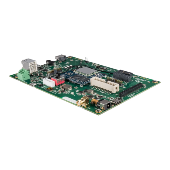
3 Open-Q 212A Development Kit 3.1 Introduction The Open-Q 212A provides a reference and evaluation platform for the Qualcomm 212 processor. This kit is suited for Linux Home Hub OS testing to evaluate, optimize, and deploy applications that utilize the Qualcomm 212 series SOC technology. -
Page 12: Getting Started
Lantronix for availability of display adaptors, camera modules, sensor boards, and other accessories: sales@lantronix.com 3.5 Getting Started This section explains how to setup the Open-Q 212A Development Kit and start using it. 3.5.1 Registration To register the development kit and gain access to the Lantronix support site, please visit: http://www.intrinsyc.com/resources. -
Page 13: Powering Up The Development Kit
Open-Q 212A Development Kit 3.5.2 Powering Up the Development Kit 1. At a static-safe workstation, remove the development kit board carefully from the anti static bag. 2. Connect the serial debug USB (17) to your favorite terminal program if you wish to see boot messages (FTDI UART —... -
Page 14: Development Kit Block Diagram
Open-Q 212A Development Kit 3.6 Development Kit Block Diagram The following diagram explains the interconnectivity and peripherals on the Open-Q 212A development platform. Note that not all HW features shown here may be supported by current SW. Switches & 212A SOM... -
Page 15: Open-Q 212A Som
Open-Q 212A Development Kit 3.7 Open-Q 212A SOM The Open-Q 212A SOM measuring in 50mm x 46.5mm is where all the processing occurs. It is connected to the carrier via three 100-pins board to board (B2B) connectors. The SOM provides the basic common set of features with minimal integration efforts for end users. -
Page 16: Som Rf Interfaces For Wi-Fi And Bluetooth Antennas
Open-Q 212A Development Kit Power Qualcomm® PM8916-1 Management Memory/Storage 1GB LPDDR3 RAM/ 4GB eMMC Flash Wireless Wi-Fi/BT module - 802.11a/b/g/n/ac, 2x2 MU-MIMO, 2.4/5Ghz, Bluetooth 4.2 + BLE (Qualcomm® QCA9379-3) 3x MHF 4 antenna connectors - Two for Wi-Fi, One for Bluetooth GNSS Qualcomm®... -
Page 17: Som Rf Interface For Gnss Antenna
Open-Q 212A Development Kit For details on how the Wi-Fi module connects to the on-board PCB antennas on the carrier board, refer to section Error! Reference source not found.. 3.7.1 SOM RF Interface for GNSS Antenna The SOM includes one U.FL type coaxial connector for the GNSS receiver antenna, with a +2.7v bias on it to provide power for an active GNSS antenna. -
Page 18: Open-Q 212A Carrier Board
Open-Q 212A Development Kit 3.8 Open-Q 212A Carrier Board The Open-Q™ 212A Carrier board measures 17cm x 11.5cm and has various connectors for different peripherals. Table 2 Open-Q 212A Carrier Board Features Feature Specification Audio • 6x Digital Mics via expansion Board •... -
Page 19: Dc Jack - J21
Open-Q 212A Development Kit Function Switc Description Notes BOOT_CONFIG[3] S10-3 APQ_GPIO_79 / BOOT_CONFIG[3] Refer to carrier board schematics for boot option OFF (Default): Low ON: High BOOT_CONFIG[2] S10-4 APQ_GPIO_78 / BOOT_CONFIG[2] Refer to carrier board schematics for boot option OFF (Default): Low... -
Page 20: Som Power Source Selection Switch - S300
Open-Q 212A Development Kit Figure 4 12V DC Power Jack (J21) 3.8.3 SOM Power Source Selection Switch – S300 Switch S300 allows the user to power the SOM using either the 12V DC power supply or a Lithium battery. See table below for selecting the correct power source for the SOM. -
Page 21: Battery Connector - J300
Open-Q 212A Development Kit MB_ELDO_CAM1_DVDD • MB_ELDO_CAM1_VCM • Note 2: See Section 3.8.4 and Section 3.8.5 for setting up the development kit to be powered by a battery Figure 5 SOM Power Source Switch (S300), Up position shown 3.8.4 Battery Connector – J300 J300 allows user to connect a single-cell rechargeable Lithium battery pack to power the development kit. -
Page 22: Battery Dip Switch - S1
Open-Q 212A Development Kit Nominal Battery Voltage 3.7V Max. Battery Voltage 4.2V Battery ID Support See Section 3.8.5 for more information Thermistor Support (10k Expected) See Section 3.8.5 for more information Table 6 Battery Connector (J300) Pinout Description Signal Pin # Connection to Battery Thermistor. -
Page 23: External Battery-Charger Header - J26
Open-Q 212A Development Kit Switch Function Description Notes Position CBL_PWR_ Auto boot Selection ON (Default): System will auto boot whenever power is applied OFF: User needs to press the power button to turn on the system after power is applied... - Page 24 Open-Q 212A Development Kit Description Signal Signal Description Battery Positive Not available on BATT_P PMI_VDD_CAP Voltage Sense 212A Battery Negative Not available on BATT_N CHG_VBAT_SNS Voltage Sense 212A Not available on Battery ID Pin BAT_ID PMI_CHG_EN 212A APQ GPIO_66 Default: SMB_EN...
-
Page 25: Power Probe Header - J86
Open-Q 212A Development Kit Description Signal Signal Description APQ GPIO_7 GPIO_7_BLSPx_I2C_ BLSP2 Bit 0 Default: I2C2_SCL APQ GPIO_6 GPIO_6_BLSPx_I2C_ +1.8V output BLSP2 Bit 1 BATT_EXP_1P8 (VREG_L5_1P8) Default: I2C2_SDA SOM_SYS_PWR_ PER (SOM Power BATT_EXP_SYS_PW Input) USB_VBUS for SOM and USB Ports... -
Page 26: Power Header - J60
Open-Q 212A Development Kit Pin # Description Signal 3.8.8 Power Header – J60 The Power Header allows user to power their peripherals from the carrier board. Please see the pinout below for voltage level. Figure 10 Power Connector (J60) Table 10 Power Header J60 Pinout... -
Page 27: Debug Serial Uart - J22
Open-Q 212A Development Kit Description Signal Signal Description CAM1 VCM MB_ELDO_CAM1_V LDO (U10) output PMI8916-1 3V3 Rail MB_VREG_3P3 VREG_L4_1P8 VREG_L4 PMI8916-1 VREG_L10_2P85 VREG_L10 PMI8916-1 VREG_L11_SDC VREG_L11 PMI8916-1 3V3 Rail MB_VREG_3P3 VREG_L4_1P8 VREG_L4 12V from J300 DC_IN_12V MB_VREG_5P0 5V LDO (U1) output 3.8.9 Debug Serial UART –... -
Page 28: Sensor Io Expansion Header - J53
Open-Q 212A Development Kit DIP Switch S10 Position 8 ‘FORCE_SW_UART’ = OFF/OPEN Serial Port Settings: Baud Rate: 115200 Data: 8 bits Parity: None Stop:1 bit Flow Control: None 3.8.10 Sensor IO Expansion Header – J53 Figure 12 J53 Sensor Expansion Header The sensor expansion header (J53) allows user to connect to an optional home automation connectivity accessory board that features the Qualcomm QCA4024 Zigbee/BLE chip. - Page 29 Open-Q 212A Development Kit Description Signal Signal Description Accelerometer interrupt SENSOR_ACCEL_ GPIO_6_BLSPx_I2 Sensor I2C SDA (APQ input (APQ GPIO_96) C_SDA GPIO_6) Interrupt input (APQ SENSOR_CAP_IN GPIO_7_BLSPx_I2 Sensor I2C SCL (APQ GPIO_65) C_SCL GPIO_7) Gyroscope interrupt SENSOR_GYRO_I GPIO_XX_SENSO Sensor reset signal...
-
Page 30: Headset Audio Jack - J27
Open-Q 212A Development Kit 3.8.11 Headset Audio Jack – J27 J27 is a standard 3.5mm TRRS jack in CTIA pinout order with headset detection support. Signals are routed to Audio CODEC WCD9326 on the SOM. This function is not supported in BSP V1.0 and maybe supported in the future BSP. - Page 31 Open-Q 212A Development Kit Table 12 Audio Input Expansion Header (J50) Pinout Note Signal Signal Note CDC_MIC1_P CDC_MIC1_N 624_DMIC0_CLK See Section 3.8.27 CDC_MIC2_P 624_DMIC0_DATA See Section 3.8.27 CDC_MIC2_N CDC_DMIC1_CLK CDC_DMIC1_DATA CDC_MIC3_P CDC_MIC3_N CDC_DMIC2_CLK CDC_MIC4_P CDC_DMIC2_DATA CDC_MIC4_N CDC_DMIC3_CLK Not Available on the 212A dev.
-
Page 32: External Codec/Gpio Expansion Header - J1
Open-Q 212A Development Kit Note Signal Signal Note PM8916-1 VREG_L5_1P8 U24 on Carrier MB_VREG_3P3 GPIO_XX_MIC_SELECT APQ GPIO_51 Board U1 on Carrier Board MB_VREG_5P0 CDC_LINE_OUT_3 CDC_LINE_OUT_REF CDC_LINE_OUT_4 3.8.13 External Codec/GPIO Expansion Header – J1 J1 allows user to access SLIMBUS, I2S, power rails, and other GPIOs from APQ or PM8916-1 that are not used by another peripheral on the carrier board. - Page 33 Open-Q 212A Development Kit Description Signal Signal Description BLSP1 bit 0 GPIO_3_BLSP1_SPI_CL MI2S_1_D3 Not Available on the 212A dev. kit (APQ GPIO 15) Can be configured as APQ GPIO_93 by installing R2111 on CB MI2S_1_D2 Not Available on the 212A dev. kit...
-
Page 34: On Board Pcb Wlan And Bt Antennas
Open-Q 212A Development Kit Description Signal Signal Description VREG_L5_1P8 U24 on Carrier MB_VREG_3P3 212_GPIO_75 General Purpose. Board GPIO 75 Carrier MB_VREG_5P0 212_GPIO_84 General Purpose. Board GPIO 84 Main 12V DC DC_IN_12V GPIO_45_AMP_FAULT General Purpose. APQ GPIO 36 GPIO_44_AMP_RST_N General Purpose. -
Page 35: Gnss Pcb Antenna And External Antenna Connections
GNSS PCB Antenna and External Antenna Connections The Open-Q 212A SOM supports GNSS function by using the Qualcomm WGR7640 GNSS Receiver. User can select either the PCB antenna on the carrier board (E4) or the external antenna connection (J41) to receive GNSS signal by toggling S10 position 1. -
Page 36: Display Connector - J2
Camera Connector – J5 J5 allows the Open-Q 212A development kit to connect to a MIPI CSI camera module. Pinout of this connector are given below. Please note that only the J5 camera port is supported on the Open-Q 212A platform. - Page 37 Open-Q 212A Development Kit Table 16 Camera Connectors (J5, J4) Pin Out Signal Note CSI0_EXT1_PWR CSI0_EXT1_PWR MB_VREG_3P3 CSI0_EXT1_PWR CSI0_AVDD VREG_L17_2P85 CSI0_DVDD VREG_L2_1P1 CSI0_ACT_VDD VREG_L10_2P85 CSI0_ACT_VDD CSI0_DOVDD VREG_L6_1P8 CSI0_DOVDD CAM_MUTE_CONN0_GND CAM0_FLASH_EN CAM1_RST_N CAM1_STANDBY_N GPIO_30_CCI_I2C_SCL0 GPIO_29_CCI_I2C_SDA0 CAM_MCLK0 CAM0_FLASH_TRIG MIPI_CSI0_LANE0_N MIPI_CSI0_LANE0_P MIPI_CSI0_CLK_N MIPI_CSI0_CLK_P...
-
Page 38: Automation Connector Header - J3100
3.8.19 Automation Connector Header – J3100 J3100 is used for automating tests on the development platform and is not supported by Lantronix for customer use. This header contains certain power rails and system control signals that users can access should they need to. *If this connector is to be used, remove R300 and disable battery source using switch S300 (see Section 3.8.3). -
Page 39: Haptic Motor Header - J802
Open-Q 212A Development Kit Figure 20 J3100 Automation connector header Table 17 Automation Connector J3100 Pin Out Pin # Signal Description VREG_MDM_1P8 VREG_L5_1P8 APQ_PS_HOLD Power supply hold signal output from APQ to USB_VBUS_DISBL Input used to disconnect VBUS from USB Ports. -
Page 40: Buttons - S100, S101, S102
Open-Q 212A Development Kit Figure 21 Haptic Motor Header (J802) Table 18 Haptic Motor Header Pinout (J802) Pin # Signal HAP_OUT_P (VPH_PWR) HAP_OUT_N (VIB_DRV_N from PM8916-1) 3.8.21 Buttons – S100, S101, S102 There are three push-buttons (S100, S101, and S102) on the carrier board to allow users to interact with the system. -
Page 41: Led Indicators - Ds1, Ds2, Ds3, Ds2320
Open-Q 212A Development Kit Table 19 Buttons Function description (S100, S101, S102) Buttons Function Description S100 Power Button System Power On, Standby S101 Volume Up Increase volume S102 Volume Down / Reset Decrease volume, hold to reset system (FW dependent) 3.8.22... -
Page 42: Usb Type C Port - J2500
Open-Q 212A Development Kit Colour Function DS2320 Green USB_HUB_ACTIVE from U2800 (USB Hub IC) to indicates hub is active 3.8.23 USB Type C Port – J2500 J2500 is standard USB 3.0 Type-C connector. This connector has no function on the 212A Development Kit. -
Page 43: Usb 2.0 Type-A Ports - J2900
Open-Q 212A Development Kit 3.8.25 USB 2.0 Type-A Ports – J2900 There are two ports USB 2.0 Type-A ports provided by the USB switch hub IC (U2800). These ports follow the industry standard and have a maximum current output of 500mA on each port. -
Page 44: Dmics
S1700 controls the DMIC and UART path. See Section 3.8.27. 3.9 Accessories 3.9.1 Camera Module Accessory A camera module is available as an optional accessory from the Lantronix online store in the Accessories section: https://shop.intrinsyc.com/ The compatible camera accessory is based on the 5MP OmniVision OV5640 sensor with YUV output and interfaces to the development kit through the included 21cm JAE interface cable to connector J5 on the development kit.
Need help?
Do you have a question about the Open-Q 212A and is the answer not in the manual?
Questions and answers