
Related Manuals for Lantronix HDK845


Summary of Contents for Lantronix HDK845
- Page 1 Snapdragon 845 HDK Hardware Development Kit User Guide Part Number PMD-00060 Revision A October 2020...
- Page 2 Fax: 949-453-3995 IES Customer Support Portal https://helpdesk.intrinsyc.com Lantronix Technical Support http://www.lantronix.com/support Sales Offices For a current list of our domestic and international sales offices, go to the Lantronix web site at http://www.lantronix.com/about-us/contact/ Snapdragon 845 HDK Hardware Development Kit User Guide...
- Page 3 Revision History Date Rev. Comments May 2018 Initial release. Intrinsyc document number: ITC-01IMP1335-UG-001 October 2020 Version information, installation instructions and package contents clarified For the latest revision of this product document, please go to: http://tech.intrinsyc.com. Snapdragon 845 HDK Hardware Development Kit User Guide...
-
Page 4: Table Of Contents
4 Processor Board Processor Board Mechanical Properties __________________________________ 15 Hardware Specification ________________________________________________ 15 5 Carrier Board Dip switch Configuration Options ________________________________________ 19 HDK845 Carrier Board Expansion Connectors _____________________________ 21 5.2.1 Power Option ____________________________________________________ 24 5.2.2 Debug Serial UART header J2103 ____________________________________ 24 5.2.3... - Page 5 Figure 6-1 HDK Display Card ........................41 Figure 6-2 Display Card Default Configuration ..................43 List of Tables Table 4-1 HDK845 Processor Board Mechanical Properties ..............15 Table 4-2 HDK845 Hardware Features ....................15 Table 5-1 HDK845 Carrier Board Mechanical Properties ................ 18 Table 5-2 Dip Switch S2301 HW / SW Configuration ................
- Page 6 Table 5-12 MIPI CSI Camera Connector Pinouts (J1701) ............... 35 Table 5-13 MIPI CSI Camera Use Cases....................38 Table 6-1 HDK845 Display Card Mechanical Properties ................. 41 Table 6-2 Display Power Domains ......................43 Snapdragon 845 HDK Hardware Development Kit User Guide...
-
Page 7: Introduction
The purpose of this user guide is to provide primary technical information on the Snapdragon 845 HDK Hardware Development Kit User Guide. For more background information on this development kit, visit: www.lantronix.com 1.2 Scope This document will cover the following items on the Snapdragon 845 Har: Block Diagram and Overview •... -
Page 8: Documents
2: Documents 2 Documents This section lists the supplementary documents for the Snapdragon Q 845 Hardware Development Kit. 2.1 Applicable Documents Reference Title Intrinsyc Purchase and Software License Agreement for the Snapdragon Development Kit 2.2 Reference Documents Reference Title 2.3 Terms and Acronyms Term and acronyms Definition AMIC... - Page 9 2: Documents Term and acronyms Definition JTAG Joint Test Action Group Low Noise Amplifier MIPI Mobile Industry processor interface Multi-Purpose Pin Near Field Communication Radio Frequency SATA Serial ATA SLIMBUS Serial Low-power Inter-chip Media Bus System Power Management Interface (Qualcomm® PMIC / baseband SPMI proprietary protocol) Single wire serial bus interface (Qualcomm®...
-
Page 10: Snapdragon 845 Hardware Development Kit
3: Snapdragon 845 Hardware Development Kit 3 Snapdragon 845 Hardware Development Kit 3.1 Introduction The Snapdragon 845 Hardware Development Kit provides a quick reference or evaluation platform for Qualcomm’s Snapdragon 845 processor. This kit is suited for Android / Linux application developers, OEMs, consumer manufacturers, hardware component vendors, video surveillance, robotics, camera vendors, and flash chip vendors to evaluate, optimize, test and deploy applications that can utilize the Qualcomm®... -
Page 11: Kit Contents
3: Snapdragon 845 Hardware Development Kit 3.4 Kit Contents The Snapdragon 845 Hardware Development Kit includes the following: Snapdragon 845 processor board with the Snapdragon 845 (SDA845) processor main CPU board Mini-ITX form-factor carrier board for I/O and connecting with external peripherals 12V power adapter USB type-C cable and charger 5.7”... -
Page 12: Hardware Identification Label
Figure 3-2 Assembled Snapdragon 845 Hardware Development Kit bottom The development kit comes with Android software pre-programmed on the CPU board or processor board. Contact Lantronix for availability of camera modules, sensor boards, and other accessories: sales@lantronix.com 3.5 Hardware Identification Label Labels are present on the processor board. -
Page 13: System Block Diagram
Figure 3-3 HDK Block diagram RFFE1 USB0_SS Type C USB1_SS USB1_HS Type A JTAG USB Hub USB2_HS Type A GPIO USB to UART QUP9 Micro B GPIO Figure 3-3 HDK845 Block Diagram Snapdragon 845 HDK Hardware Development Kit User Guide... -
Page 14: Processor Board
Figure 4-1 HDK Processor Board The HDK845 processor board is where all the processing occurs. It is connected to the carrier board via two 240-pin high speed board-to-board connector. The purpose of the connectors is to bring out essential signals such that other peripherals can interface with the platform. -
Page 15: Processor Board Mechanical Properties
4: Processor Board 4.1 Processor Board Mechanical Properties Table 4-1 HDK845 Processor Board Mechanical Properties 42 cm (60 mm x 70 mm) Dimension two 240-pin high speed board-to-board connector Interface A top side heat sink and a bottom side heat conductive metal plate are Thermal installed by default. - Page 16 4: Processor Board Subsystem / Connectors Feature Set Description Specification PMIC (PM845, PM8005 Qualcomm® PMIC, Companion PM845 -- Primary core PMIC for SDA845 processor PMIC. PON, POFF, and &PMI8998) reset master. Generates system clocking and tightly coupled chipset power. PM8005 -- Secondary core PMIC.
- Page 17 4: Processor Board Subsystem / Connectors Feature Set Description Specification 1x WiGig Connect to antenna on 802.11ad-60 GHz processor board via coax cable Audio 1 x Headset Output Headset/ headphone output Analog differential output 2 x Loud-speaker 2 x loud-speaker output Digital output 1 x Earpiece output Earpiece output...
-
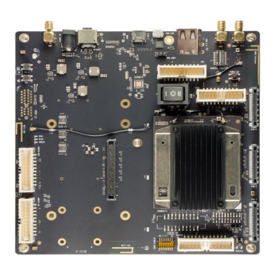
Page 18: Carrier Board
5: Carrier Board 5 Carrier Board The HDK845 Carrier board is a Mini-ITX form factor board with various connectors used for connecting different peripherals. The following are the mechanical properties of the carrier board: Table 5-1 HDK845 Carrier Board Mechanical Properties... -
Page 19: Dip Switch Configuration Options
5: Carrier Board 5.1 Dip switch Configuration Options There is one DIP switch S2301 on the south top side of the HDK845 carrier board. The 8-bit switch allows the user to control the system configuration and boot options. Table below outlines... -
Page 20: Table 5-3 Dip Switch S2302 Hw / Sw Configuration
HDMI by turning on DIP display card There is another DIP switch S2302 on the north top side of HDK845 carrier board. The 8-bit switch allows the user to control the system configuration and boot options. Table 5-3 Dip Switch S2302 HW / SW configuration... -
Page 21: Hdk845 Carrier Board Expansion Connectors
Before making any changes to the dip switch, make sure to note down the previous WARNING configuration. 5.2 HDK845 Carrier Board Expansion Connectors The table below lists the connectors, expansions and their usages on the carrier board: Table 5-4 Carrier Board Expansion options and their usage... - Page 22 5: Carrier Board Domain Description Specification Usage 3-Digital Microphone via Audio expansion Digital Audio header For Digital audio input for audio input expansion Digital MIC, I2S codec, Slim Supported by WCD9340 header bus interface. 3-Analog Microphone via Audio expansion Analog Audio header For Analog audio input for audio input expansion Analog MIC (differential...
- Page 23 The information listed below is of particular use for those who want to interface other external hardware devices with the HDK845. Before connecting anything to the development kit, ensure the device meets the specific hardware requirements of the processor.
-
Page 24: Power Option
5: Carrier Board Power Option The HDK development kit power source connects to the 12V DC power supply jack J0701. Starting from the power jack, the 12V power supply branches off into different voltage rails via step down converters on the carrier board and PMIC on the Processor board. -
Page 25: Debug Serial Uart Over Usb J2102
Figure 5-4 J2102 Debug UART over USB The UART connection used on the HDK845 is a USB micro B connector (J2102). This debug UART is available over USB via the FTDI FT232RQ chip on the carrier board. To get the serial terminal working with a PC, user needs to ensure that the appropriate FTDI drivers are installed. -
Page 26: Table 5-6 Jtag Header J2101 Pin Out
5: Carrier Board Table 5-6 JTAG Header J2101 Pin out Description Signal Pin NO Description Signal Pin NO J2101[2] JTAG Power JTAG_PWR J2101[1] detect J2101[4] Target TRST_N J2101[3] RESET_N signal J2101[6] TDI Signal J2101[5] (Target DATA J2101[8] TMS Signal J2101[7] J2101[10] TCK Signal J2101[9]... -
Page 27: Sensor Io Expansion Header J2501
5: Carrier Board Sensor IO Expansion Header J2501 Figure 5-6 J2501 Sensor Expansion Header The sensor expansion header J2501 allows for a 24-pin connection to an optional sensor board. If user application does not require a sensor, then this header can be used for other applications that require I2C or GPIO input and output connections. -
Page 28: Nfc Expansion Header J2401
5: Carrier Board Description Signal Pin NO Description Signal Pin NO SSC SPI-1 SSC_SPI1_CS J2501[13] Alternate sensor ALSP_INT_N J2501[14] interrupt input to processor via chip select 2 GPIO120 MISC GPIO SDA_GPIO62 J2501[15] Digital Compass MAG_DRDY_I J2501[16] interrupt input to processor via GPIO119 sensor via GPIO62... -
Page 29: Headset Jack J1501
5: Carrier Board Table 5-8 NFC Expansion Header J2401 pin out Description Signal Pin NO Description Signal Pin NO QUP0 NFC_SPI_CLK J2401[1] QUP0 NFC_SPI_MIS J2401[2] NFC power NFC_ESE_PW J2401[3] SIM present UMI1_DET_N J2401[4] request via R_REQ GPIO via SDA GPIO116 GPIO112 SIM Card DATA UIM1_DATA... -
Page 30: Audio Inputs Expansion Header J1601
5: Carrier Board Audio Inputs Expansion Header J1601 Figure 5-9 J1601 Audio Inputs Expansion Header This header expansion provides the following audio inputs: 3 digital mics 3 analog mics Voltage rails to support analog and digital mics The table below outlines the pin out information of the audio inputs expansion header J1601: Table 5-9 Audio Inputs Expansion Header J1601 Pin out Description... -
Page 31: Audio Outputs Expansion Header J1602
5: Carrier Board Audio Outputs Expansion Header J1602 Figure 5-10 J1602 Audio Outputs Expansion Header This header expansion provides the following audio outputs: 2 differential analog audio line out 2 single ended analog audio line out 1 differential analog earpiece amplifier output (no external amp needed) ... -
Page 32: Usb Type A Connector J1101
5: Carrier Board Description Signal Pin NO Description Signal Pin NO Analog CDC_EAR_P J1602[9] Analog CDC_EAR_M J1602[10] earpiece earpiece amplifier out, amplifier out, positive negative differential differential output output J1602[11] 3.8V output VPH_PWR J1602[12] power supply Digital sound CDC_SWR_ J1602[13] Digital sound CDC_SWR_D J1602[14]... -
Page 33: Usb3.1 Type C Connector J1201
DisplayPort V1.3 On Board PCB WLAN Antenna The HDK845 carrier board has two on-board PCB antennas that connects to the WCN3990 WiFi module on the processor board via coaxial cables that attaches to MH4L receptacles. These antennas connect to the processor board in the following configuration: •... -
Page 34: On Board Pcb Gnss Antenna
On Board PCB GNSS Antenna Figure 5-13 GNSS On Board PCB GNSS Antennas The HDK845 carrier board has one on-board PCB antennas on the bottom side that connects to the Processor board via coaxial cable that attaches to MH4L receptacles. The on-board antenna is connected to the Processor board by default, meanwhile, there are 0-ohm jumpers for user to use an external GNSS antenna via the SMA connector. -
Page 35: Camera Connector
5: Carrier Board Camera connector The HDK845 development kit supports three 4-lane MIPI camera interfaces via a 120pin connector, it also supports one 2-lane MIPI camera interface via a 23-pin connector on the Processor board. The following are some features of the camera connectors: 3 x 4 lane MIPI CSI signals, CSI0, CSI1 and CSI2 ... - Page 36 5: Carrier Board Pin# Signal Description Pin# Signal Description FLASH_LED2 FLASHLED2 CAM_ELDO4_EN PM845 GPIO9 FLASH_LED2 FLASHLED2 CAM_ELDO1_EN PM845 GPIO12 DGND DGND FLASHLED3 FLASH_LED3 FLASH_LED3 FLASHLED3 FLASH_R3LED_EN PMI8998 GPIO3 DGND DGND MIPI_CSI2_LANE3_N CSI2 data FLASH_FRONT_EN SDA GPIO21 MIPI_CSI2_LANE3_P CSI2 data FL_STROBE_TRIG SDA GPIO22 DGND DGND...
- Page 37 5: Carrier Board Pin# Signal Description Pin# Signal Description MIPI_CSI2_LANE2_P CSI2 data P1V2_DVDD_CAM1_2 1.2V power supplier DGND DGND CSI2 data 2.85V power MIPI_CSI2_LANE1_N P2V85_AVDD_CAM1_2 supplier MIPI_CSI2_LANE1_P CSI2 data P2V85_AVDD_CAM1_2 2.85V power supplier DGND DGND CSI2 data 2.8V power MIPI_CSI2_LANE0_N P2V8_VCM_LASER_RF supplier MIPI_CSI2_LANE0_P CSI2 data...
-
Page 38: Vertigo Sensor Connector
Three 4-lane CSI (4+4+4 or 4+4+2+1) CPHY Three 3-trio CPHY1.0 Vertigo Sensor connector The HDK845 development kit supports a 30-pin connector (449-53935-0030) to support Vertigo 10 or follow on card, same as CDP845. Snapdragon 845 HDK Hardware Development Kit User Guide... -
Page 39: Hdmi Connector
Figure 5-16 Vertigo Connector (J1701) HDMI Connector The HDMI type A connector enables the HDK845 development platform to connect to an external HDMI monitor/ television via an HDMI cable. The LT9611 MIPI DSI to HDMI1.4 bridge IC features a resolution up to 4K30Hz. -
Page 40: Pci Express 1X Slot (Reserve)
PCI Express 1X Slot (Reserve) The PCI Express slot (J2701) used on the HDK845 development kit is a standard PC style half-height card slot. It allows for external peripheral connectivity such as Gigabit Ethernet, Gigabit Wi-Fi, or PCIe based audio / video processors. -
Page 41: Display Card
100-pin high speed board-to-board connector Major Interfaces Figure 6-1 HDK Display Card 6.1 HDK845 Display Card Overview The display output options for the HDK845 Development Kit consists of A 100-pin display connector J0501 that supports: Dual DSI DPHY 1.2 ... -
Page 42: Display Card Connector J0501
6: Display Card The HDK845 development platform can support the following display combinations: MIPI DSI 1 x 4-lane DSI0 + 1 x 4-lane DSI1 2 x 4-lane DSI DPHY 1.2 6.2 Display Card Connector J0501 The 100-pin display card connector provides the following features/ pin-outs that enables the development kit to... -
Page 43: Figure 6-2 Display Card Default Configuration
Carrier 12 V up to 0.5A HDK845 display card (part number: 20-PB892-H10) is an additional PCBA that mates with the display connector J1301 on the carrier board. This board allows users to interface with the development kit via the LCD (see below for details) that comes preinstalled on the display card. Figure 6-2 Display Card Default Configuration, illustrates the interfacing connectors on the display card. -
Page 44: Lcd Panel
6: Display Card 6.3 LCD panel The LCD panel comes preinstalled on the HDK845 display card Below are the Panel specifications: Resolution: QHD 2560x1440 LCD Type: TFT PCAP touch panel No of Lanes: 2 x 4 lane MIPI DSI interface via Display Card ...
Need help?
Do you have a question about the HDK845 and is the answer not in the manual?
Questions and answers