
Related Manuals for Lantronix Open-Q 2100


Summary of Contents for Lantronix Open-Q 2100
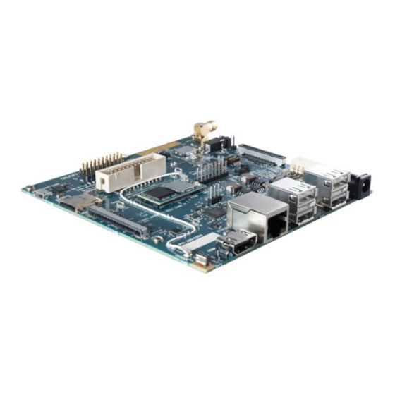
- Page 1 Open-Q™ 2100 Development Kit User Guide Part Number PMD-00069 Revision A August 2020...
- Page 2 Phone: 949-453-3990 Fax: 949-453-3995 IES Customer Support Portal https://helpdesk.intrinsyc.com Lantronix Technical Support http://www.lantronix.com/support Sales Offices For a current list of our domestic and international sales offices, go to the Lantronix web site at http://www.lantronix.com/about-us/contact/ Open-Q™ 2100 Dev Kit User Guide...
- Page 3 Fixed error in Wi-Fi specification Updated cover photo August 2020 Initial Lantronix document. Added Lantronix document part number, Lantronix logo, branding, contact information, and links. For the latest revision of this product document, please go to: http://tech.intrinsyc.com. Open-Q™ 2100 Dev Kit User Guide...
-
Page 4: Table Of Contents
Hardware Identification Label __________________________________________ 12 Getting Started _____________________________________________________ 12 3.6.1 Default DIP switch settings _________________________________________ 13 3.6.2 Powering up the Open-Q 2100 Development Kit ________________________ 13 3.6.3 Changing Display Output __________________________________________ 14 System Block Diagram _______________________________________________ 14 Open-Q 2100 SOM __________________________________________________ 16 3.8.1... - Page 5 3.9.14 Display Connector J2300 _________________________________________ 35 3.9.15 Camera Connector J2500 _________________________________________ 39 3.9.16 USB 2.0 Client Port J2800 ________________________________________ 42 3.9.17 USB 2.0 host interface ___________________________________________ 42 3.9.18 Coin cell battery holder ___________________________________________ 43 3.9.19 FM connector J1801 _____________________________________________ 43 3.9.20 Micro-SD card connector J1900 ____________________________________ 43 3.9.21...
-
Page 6: Introduction
• Configuration • • Carrier Board • Display Board for LCD (Optional) 1.3 Intended Audience This document is intended for users who would like to develop custom applications on the Open-Q 2100 Development Kit. Open-Q™ 2100 Dev Kit User Guide... -
Page 7: Documents
Documents 2 Documents This section lists the supplementary documents for the Open-Q 2100 Development Kit. 2.1 Applicable Documents Reference Title Intrinsyc Purchase and Software License Agreement for the Open-Q Development 2.2 Reference Documents Reference Title Hardware Document Set for the Qualcomm APQ8009W based on Open-Q... - Page 8 Documents Term and acronyms Definition Global Positioning system HDMI High Definition Media Interface HSIC High Speed Inter Connect Bus JTAG Joint Test Action Group Low Noise Amplifier MIPI Mobile Industry processor interface Multi-Purpose Pin Near Field Communication Radio Frequency SATA Serial ATA SLIMBUS Serial Low-power Inter-chip Media Bus...
- Page 9 List of Figures Figure 1 Open-Q 2100 Development Kit ....................12 Figure 2 Cable connection and DIP switches on the Open-Q 2100 Dev kit ........13 Figure 3 Open-Q 2100 SOM + Carrier Board Block Diagram .............. 15 Figure 4 Open-Q 2100 SOM ........................ 16 Figure 5 SOM Block Diagram .......................
- Page 10 Documents Table 3.9-6 Sensor Expansion Header J2600 Pin out ................. 29 Table 3.9-7 Digital IO (low speed) Expansion Header J2601 Pin out ..........31 Table 3.9-8 Audio IO Expansion (PMIC) Header J3600 Pin out ............32 Table 3.9-9 MIPI CSI Camera Connector J2500 Pin out ..............39 Table 3.9-10 Power probe J202 Pin out ....................
-
Page 11: Open-Q 2100 Development Kit
3 Open-Q 2100 Development Kit 3.1 Introduction The Open-Q 2100 Development Kit provides a reference platform for Qualcomm’s latest 2100 series - Qualcomm® 2100 processor. This kit is suited for Android / Linux application developers, OEMs, consumer manufacturers, hardware component vendors, video surveillance, robotics, camera vendors, and flash chip vendors to evaluate, optimize, test and deploy applications that can utilize the Qualcomm®... -
Page 12: Hardware Identification Label
To register a development kit, please visit: https://tech.intrinsyc.com/account/register Note: Please retain the SOM and carrier board serial number for warranty purposes. 3.6 Getting Started The instruction in this section explains how to setup the Open-Q 2100 Development Kit. Open-Q™ 2100 Dev Kit User Guide... -
Page 13: Default Dip Switch Settings
J2800, microB USB (recovery/ ADB port) J3000 (DC IN) Figure 2 Cable connection and DIP switches on the Open-Q 2100 Dev kit 3.6.2 Powering up the Open-Q 2100 Development Kit To power-up the board, perform the following steps below: 1. At a static-safe workstation, remove the development kit board carefully from the anti-static bag. -
Page 14: Changing Display Output
Changing Display Output The Open-Q 2100 Dev Kit is shipped pre-configured to HDMI display. If you need to change the display output between LCD and HDMI, use the following commands to switch the display. Note that you also must switch the HDMI/DSI select DIP switch. -
Page 15: Figure 3 Open-Q 2100 Som + Carrier Board Block Diagram
SSCs / GPIOs / IRQs 1 x Headset Connector User/ Configuration Speed BPLSs / GPIOs Switch Expansion GPIOs Header TTL to UART Carrier Board Figure 3 Open-Q 2100 SOM + Carrier Board Block Diagram Open-Q™ 2100 Dev Kit User Guide... -
Page 16: Open-Q 2100 Som
3.8.2 SOM Block Diagram The Open-Q 2100 SOM measuring 31.5mm x 15mm is where all the processing occurs. It is connected to the carrier board via two 100 pin Hirose DF40 connectors. The purpose of these connectors is to bring out essential signals such that other peripherals can be connected to the platform. -
Page 17: Hardware Specification
USB HS SPI/ I2C Open-Q™ 2100 System on Module Figure 5 SOM Block Diagram 3.8.3 Hardware Specification The Open-Q 2100 SOM platform encompasses the following hardware features: Table 3.8-2 Open-Q 2100 SOM Hardware Features Subsystem / Feature Set Description Specification... - Page 18 Open-Q 2100 Development Kit Subsystem / Feature Set Description Specification Connectors BT 2.4 GHz via WCN3620 Support BT 4.0 WCN3620 Wi-Fi + BT Combo Chip GNSS via GNS Receiver Frontend GPS, GLONASS, COMPASS WGR7640 – SSBI Qualcomm® Proprietary Protocol RF Interfaces...
-
Page 19: Som Rf Specification For Wifi, Bt, Gnss
Antenna 1 Antenna 2 Figure 6 Open-Q 2100 SOM Antenna locations Antenna 1: Antenna 1 is used for providing Wi-Fi and Bluetooth connectivity to WCN3620. This antenna is meant to be connected to the carrier board via a coaxial cable or to an external antenna. The WCN3620 requires an antenna to be connected here for correct operation. -
Page 20: Open-Q 2100 Som Carrier Board
Open-Q 2100 Development Kit 3.9 Open-Q 2100 SOM Carrier Board The Open-Q 2100 SOM Carrier board is a nano-ITX form factor board with various connectors used for connecting different peripherals. The following are the mechanical properties of the carrier board: Table 3.9-1 Open-Q 2100 SOM Carrier Board Mechanical Properties... -
Page 21: Dip Switch S3400 Configuration Options
Figure 8 S3400 DIP switch There is a DIP switch S3400 on the top side of the Open-Q 2100 SOM carrier board. The 4-bit switch allows the user to control the system configuration. Table 3.9-2 below outlines the pin outs and connections of this DIP switches. -
Page 22: Dip Switch S1700 Configuration Options
Figure 9 S1700 DIP switch There is a DIP switch S1700 on the top side of the Open-Q 2100 SOM Carrier Board. The 2-bit switch allows the user to control the system configuration and boot option. Table 3.9-3 below outlines the pin outs and connections of this DIP switches. -
Page 23: Carrier Board Expansion Connectors
OFF. USB (GPIO37) when DIP switch is NOTE: FORCE USB boot option turned ON for boot recovery purposes. is reserved for use by Lantronix only for boot recovery purposes. BOOT S1700-2 Enables APQ boot configuration 1 Default out of the box CONFIG1 when DIP switch is turned ON. - Page 24 Open-Q 2100 Development Kit Domain Description Specification Usage Power Button SMD Button Power Button for Suspend / Resume and Power off Volume Keys Volume + key SMD Button Volume +Key Volume – key SMD Button Volume –/ RESET Key Sensor IO Connector...
- Page 25 Open-Q 2100 Development Kit Domain Description Specification Usage USB Recovery USB 2.0 via USB-HS Micro B connector USB recovery/ debug through USB switch with battery charging support Ethernet 10/100 Ethernet MAC with RJ45 Ethernet connector Supports 10/100 full- full-duplex support via...
-
Page 26: Dc Power Input J3000
3.9.4 DC Power Input J3000 The Open-Q 2100 Development Kit power source connects to the 12V DC power supply jack J3000. Starting from the power jack, the 12V power supply branches off into different voltage rails via step down converters on the carrier board and PMIC on the SOM. -
Page 27: Battery Header J3200
Figure 12 J3200 Battery Header The Open-Q 2100 Development Kit platform can also power the SOM with a single cell Lithium-Ion Polymer (LiPo) battery pack which connects to header J3200. The purpose of this header is to be used by the end user to develop a battery charging solution, including battery characterization. -
Page 28: Debug Serial Uart Over Usb J2700
Figure 13 J2700 Debug UART over USB The UART connection used on the Open-Q 2100 SOM is a USB micro B connector (J2700). This debug UART is available over USB via the FTDI FT232RQ chip on the carrier board. To get the serial terminal working with a PC, user needs to ensure that the appropriate FTDI drivers are installed. -
Page 29: Sensor Io Expansion Header J2600
Open-Q 2100 Development Kit 3.9.7 Sensor IO Expansion Header J2600 Pin 1. Figure 14 J2600 Sensor Expansion Header The sensor expansion header J2600 allows for a 24-pin connection to an optional sensor board. If user application does not require a sensor, then this header can be used for other applications that require I2C or GPIO input and output connections. - Page 30 Open-Q 2100 Development Kit Description Signal Pin NO Description Signal Number Sensor IO PWR SENS_IO_PWR J2600 [7] Sensor Analog SENS_ANA_P J2600[8] 1.8 V power supply VREG_L6_1P8 from power supply VREG_L17_2 regulator (Digital) J2600[9] J2600[10] Test Point/ GPIO GPIO_72 J2600[11] Test Point/...
-
Page 31: Digital Io (Low Speed) Expansion Header J2601
Open-Q 2100 Development Kit 3.9.8 Digital IO (Low Speed) expansion header J2601 Pin 1. Figure 15 J2601 Digital IO (low speed) expansion header Digital IO (low speed) expansion header J2601 is a 20-pin connector that provides access to BLSP2/ BLSP1 signals. -
Page 32: Audio Io Expansion (Pmic) Header J3600
Open-Q 2100 Development Kit Description Signal Pin NO Description Signal Number Multipurpose pin 4 PMIC_MPP_4 J2601[15] Multipurpose pin 3 PMIC_MPP_3 J2601[16] from PMIC from PMIC GPIO 49 GPIO_49_US J2601[17] GPIO 69 GPIO_69_USER J2601[18] ER_LED1 _LED2 J2601[19] J2601[20] 3.9.9 Audio IO Expansion (PMIC) Header J3600 Pin 1. -
Page 33: Headset Jack J3702
On Board PCB mount WLAN Antenna The Open-Q 2100 SOM carrier board has one on-board WLAN PCB mount antenna that connects to the WCN3620 Wi-Fi module on the SOM via a coaxial cable that attaches to the U.FL receptacles. This antenna connects to the SOM in the following configuration: Open-Q™... -
Page 34: Open-Q 2100 Display
Antenna Figure 18 On Board PCB mount antenna connection 3.9.12 Open-Q 2100 Display The display output options for the Open-Q 2100 Development Kit consists of: An HDMI type A connector • HDMI (720p 60Hz) A 51-pin display connector J2300 that supports: •... -
Page 35: Hdmi Connector J2400
HDMI monitor/ television via an HDMI cable. As part of a new feature, the Qualcomm® 2100 Series (APQ8009W) can now support up to 720p HD (1280 x 720 at 60fps) Please note that the Open-Q 2100 Development Kit is for evaluation purposes only and may not be HDMI compliant. - Page 36 LCD that comes preinstalled on the display board. The following figure illustrates the interfacing connectors on the display board. Note: The display board comes as an additional add-on to the Open-Q 2100 Development Kit. To purchase this, please visit http://shop.intrinsyc.com...
-
Page 37: Figure 21 Display Board
Open-Q 2100 Development Kit Figure 21 Display Board Open-Q™ 2100 Dev Kit User Guide... -
Page 38: Figure 22 Display Board Default Configuration
Open-Q 2100 Development Kit Connecting the Display Board to the Development Kit This configuration allows the user to use the LCD display that comes with the display adaptor board. As shown in the picture below, the MIPI DSI0 lines, which come from the 51-pin JF08 connector, directly connects to the LCD panel via flex cable (part number: JF08R0R051020MA). -
Page 39: Camera Connector J2500
Contact sales@lantronix.com for more information • Note: The display above when mounted on the Lantronix Open-Q Display Adapter is meant to work with the carrier board. Altering the use of this LCD panel is not recommended. 3.9.15 Camera Connector J2500 The Open-Q 2100 Development Kit supports one 2-lane MIPI CSI camera interfaces via a JAE 41-pin connector. - Page 40 Open-Q 2100 Development Kit Pin# CAM0 (J2500) Description 1, 2, 3 SBC_VREG_3P3 Power output. Connected to main +3.3V SBC_VREG_3P3 max current 700mA. Default use is for camera flash. Ground VREG_L17A_2P85 Power output. Connected to PM8916-1 VREG_L17A regulator. Default is +2.85V. Maximum current 300mA. Default use is for camera AVDD.
- Page 41 Open-Q 2100 Development Kit Pin# CAM0 (J2500) Description Ground MIPI_CSI0_CLK_N Input. MIPI CSI0 clock lane MIPI_CSI0_CLK_P Input. MIPI CSI0 clock lane Ground MIPI_CSI0_LANE1_N Input. MIPI CSI0 data lane 1 MIPI_CSI0_LANE1_P Input. MIPI CSI0 data lane 1 Ground 29, 30 Not Connected...
-
Page 42: Usb 2.0 Client Port J2800
Open-Q 2100 Development Kit 3.9.16 USB 2.0 Client Port J2800 Figure 24 J2800 USB2.0 for ADB J2800 allows the development kit to communicate with a host PC using the Android Debug Bridge (ADB). This port is a client mode port only. This port is also used for charging battery. -
Page 43: Coin Cell Battery Holder
3.9.18 Coin cell battery holder Figure 26 B1300 Coin cell holder B1300 coin cell holder allows user to use ML614 Coin cell (Not shipped with the Open-Q 2100 Development kit) for supplying power to the SOM VCOIN power input. 3.9.19... -
Page 44: Ethernet Connector J2801
Pin 1. Figure 30 J202 Power probe connector J202 (Power probe connector) provides method of measuring power consumption of Open-Q 2100 SOM. The 0.01R sense resistor is placed in series on the VPH_PWR rail to provide method of current consumption measurement. -
Page 45: Gnss External Antenna Connector J3501
Figure 31 J3501 GNSS external antenna connector The Open-Q 2100 carrier board has both PCB antenna and external antenna connector (SMA). User can switch between PCB antenna and external antenna by using DIP switch S3500. The configuration of the DIP switch is given in the table below.
Need help?
Do you have a question about the Open-Q 2100 and is the answer not in the manual?
Questions and answers